Note: Descriptions are shown in the official language in which they were submitted.
CA 02684794 2014-12-09
SYMMETRICAL RF POWER SUPPLY FOR
INDUCTIVELY COUPLED ELECTRODELESS LAMPS
Background of the Invention
The present invention is directed to a radio frequency (RF) power supply for
operating an
electrodeless lamp, such as a fluorescent, molecular, or high intensity
discharge electrodeless
lamp. An RF power supply converts a DC voltage to a suitable radio frequency
for the lamp and
is typically part of the electronic ballast of the lamp. The RF power supply
includes a ballasting
inductor that is coupled to the electrodeless lamp to ignite and maintain the
plasma in the lamp's
discharge gas, without providing electrodes in the lamp bulb.
Because the complete electronic ballast includes numerous components in
addition to
the RF power supply (e.g., EMI filter, rectifier, PFC boost stage, DC bus
electrolytic
capacitors), the efficiency of the RF power supply is desirably 95% or more,
which has not
been achievable in a commercially available power supply. It has been found
that one of the
key factors in improving efficiency is reducing power loss in the ballasting
inductor that is
coupled to the lamp.
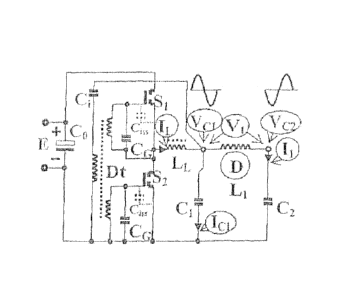
Figure 1 shows a known circuit for an RF power supply whose efficiency is
about 91.7%.
DC power source E delivers a DC voltage to a pair of DC rails, with a
1
CA 02684794 2009-10-21
WO 2008/140932
PCT/US2008/061867
electrolytic capacitor (parasitic inductance) Co. During operation, first
inductor L1 is
inductively coupled to lamp D. Transistors S1 and S2 are driven with a
sinusoidal voltage
(8-9Vp) delivered by driving transformer Dt that is tuned to a specific
frequency
(2.6MHz) by capacitors Cp, CG, and C,õ. Feedback capacitor Ci couples driving
transformer Dt with the output voltage VI. Resonance capacitor CR is parallel
to the first
inductor L1 and coupling capacitor Cc connects the output of the driving
transformer Dt
to one of the input terminals of first inductor L1 through the ballasting
inductor LL. The
resonant circuit is tuned on a frequency fRs (about 2.45MHz) that is slightly
lower than
the resulting operation frequency (fo 2.5MHz). This RF power supply has a
13.5W
loss, of which 7.8W are attributed to the ballasting inductor LL. This circuit
is further
explained in U.S. Patent 5,962,987. The particular parameters for this circuit
are shown
= in Table 1 (in Figure 5) that includes operating characteristics for RF
power supplies of
the prior art (Figures 1-2) and of the present invention (Figures 3-4) for a
same set of
input parameters so that results can be easily compared.
Figure 2 shows a variation of the circuit of Figure 1 in which the voltage
viewed
by the half bridge (the voltage VG on CR) is reduced by inserting an
additional capacitor
Cs in series with the first inductor LI, thereby avoiding the bulky coupling
capacitor Cc.
This reduces the inductance of ballasting inductor LL and thereby reduces the
losses in
the ballasting inductor LL. The voltage drop on Cs is Vcs = liXcs, which in
this instance
is about 190V. This reduces the viewed voltage VG on CR from 550V to 360V,
which is
a 35% reduction. This, in turn, reduces the inductance of ballasting inductor
LL by 35%
from 371.1H to 241.tH. The current in ballasting inductor LL can also be
reduced from
3.8App to 3.4App by reducing the phase angle between IL and the fundamental
sine wave
2 '
SUBSTITUTE SHEET (RULE 26)
CA 02684794 2015-11-17
Vof contained in the half bridge midpoint voltage, which is trapezoidal in
consequence of ZVS.
As a result, the loss in the ballasting inductor is reduced to about 4.4W
(with a further 3.6W loss
in transistors S1 and S2) so that the total loss is 9.4W, thereby increasing
the efficiency from 91.7
to 94.1%. This circuit is further explained in U.S. Patent 5,446,350. The
particular parameters
for the circuit of Figure 2 are also shown in Table 1.
Summary of the Invention
An object of the present invention is to provide a novel RF power supply for
an
electrodeless lamp that has an efficiency of at least 95%.
A further object of the present invention is to provide a novel RF power
supply for an
electrodeless lamp in which the lamp's induction coil (the first inductor L1)
is connected in a
symmetrical it-filter to further reduce the loss in the ballasting inductor
LL.
A yet further object of the present invention is to provide a novel RF power
supply for
an electrodeless lamp that includes a pair of DC rails, an RF inverter having
power input
terminals connected between the rails, a first inductor arranged to
inductively couple with an
electrodeless lamp, where the symmetrical it-filter includes first and second
resonance
capacitors that each connects a respective one of two input terminals of the
first inductor to a
same first rail of the pair of DC rails, and a second (ballasting) inductor
connecting an output of
the RF inverter to one of the two input terminals of the first inductor.
According to an aspect, there is provided a radio frequency power supply for
an
electrodeless lamp, comprising: a pair of DC rails; an RF inverter having
power input terminals
connected between the pair of DC rails; a first inductor arranged to
inductively couple with the
electrodeless lamp; first and second resonance capacitors that each connects a
respective one of
two input terminals of the first inductor to a same first rail of the pair of
DC rails; third and fourth
resonance capacitors that each connects a respective one of the two input
terminals of the first
3
CA 02684794 2015-11-17
inductor to a same second rail of the pair of DC rails; two feedback
capacitors that each connects
a driving transformer of the RF inverter to a respective one of the pair of DC
rails; a further
capacitor connected between a first node between the first and second feedback
capacitors and a
second node between the first and third resonance capacitors; and a second
inductor connecting
an output of the RF inverter to one of the two input terminals of the first
inductor.
3a
CA 02684794 2009-10-21
WO 2008/140932
PCT/US2008/061867
These and other objects and advantages of the invention will be apparent to
those
of skill in the art of the present invention after consideration of the
following drawings
and description of preferred embodiments.
Brief Description of the Drawings
Figure 1 is a circuit diagram of an RF power supply of the prior art.
Figure 2 is a circuit diagram of another RF power supply of the prior art.
Figure 3 is a circuit diagram of an embodiment of the RF power supply of the
present invention.
Figure 4 is a circuit diagram of a second embodiment of the RF power supply of
the present invention.
Figure 5 shows Table 1.
Figure 6 shows a variation of the second embodiment of the RF power supply of
the present invention.
Description of Preferred Embodiments
With reference now to Figure 3, in the present invention an RF power supply
for
an electrodeless lamp D includes a pair of DC rails receiving DC power from DC
power
source E, an RF inverter having power input terminals connected between the
pair of DC
rails (the inverter including driving transformer Dt and transistor switches
Si and S2), a
first inductor Li inductively coupled with lamp D, first and second resonance
capacitors
C1 and C2 that each connects a respective one of two input terminals of first
inductor L1
to a same first rail of the pair of DC rails, and a second (ballasting)
inductor LL
4
= St.TBSTITUTE SHEET (RULE 26).
CA 02684794 2009-10-21
WO 2008/140932
PCT/US2008/061867
connecting an output of the RF inverter to one of the two input terminals of
first inductor
LI. The RF inverter may be either a full bridge or a half bridge inverter.
Operating characteristics for the embodiment of Figure 3 are shown in Table 1
(in
Figure 5) for the same input parameters as Figures 1 and 2 so that a direct
comparison
can be made. The operating characteristics listed in Table 1 will be
appreciated by those
of skill in the art and need not be explained in detail. However, it should be
noted that
the loss in the ballasting inductor is reduced to 2.7W (and the loss in
switches S1 and S2
to 2.4W) so that the efficiency increases to 96.0%
As is apparent, the lamps inductor, first inductor LI, is connected in a
symmetrical
7c-filter and thereby supplied by two equal but phase-opposite voltages Vci
and Vc2.
Their sum is the lamp voltage VI. Lamp current is the current in second
resonance
capacitor C2; i.e., II = IC2. In the example with the input parameters from
Table 1, the
half bridge sees only half of V1 (277V) and the second (ballasting) inductor
LL has only
18.401. Continuing this example and with further reference to Table 1, the
current IL =
1.13A is the vectorial sum of Ici = 3.1A and II = 2.25A, but is the smallest
one, which is
3.2App. In this configuration with 2.7W loss in second inductor LL, 2.4W loss
in
switches S1 and S2, 0.4W loss in Dt, and 0.3W loss in resonance capacitors C1
and C2, the
total loss is 6.3W, so that efficiency reaches 96%.
This arrangement is particularly suited for electrodeless lamps with a low
power
factor (PF = cowl <0.2) because of the low magnetic coupling between the
induction
coil and the plasma. The suitability may also be enhanced by the low coil
inductance and
the low operation frequency.
SUBSTITUTE SHEET (RULE 26)
CA 02684794 2009-10-21
WO 2008/140932
PCT/US2008/061867
The present invention affords a further advantage in that the HF potentials
applied
to the first inductor L1 are halved so that the ion bombardment of the
phosphors in the
lamp are reduced fourfold. This provides a longer life for the lamp and
reduces lamp
maintenance. One additional advantage related to EMI suppression is that only
half the
RF potential is against ground, which eases the common-mode interference
suppression
within the lamp ballast. Thus, in some lamps, the E-field compensating bifilar
induction
coil can be avoided.
Figure 4 shows a further embodiment of the RF power supply of the present
invention. In this embodiment, the resonance capacitors C1 and C2 are split
and
connected to respective DC rails. That is, the power supply includes third and
fourth
resonance capacitors that each connects a respective one of the two input
terminals of the
= first inductor L1 to a same second rail of the pair of DC rails
(different than the rail to
which C1 and C2 are connected in the first embodiment.) In a similar manner,
the
feedback capacitor C, can be split and connected to opposite rails. This
arrangement
reduces the high frequency ripple current in the electrolytic capacitor Co and
eases once
more the EMI suppression.
Further, a low-pass filter, including capacitor Cf and inductor Lf, can be
added to
filter the remainitig interference at 2.5MHz due to ESR so that the parasitic
inductance Co
can be filtered to make the RF power supply neutral from the conducted EMI
point of
view.
Significantly, the circuit of Figure 4 also reduces the considerable losses in
Co by
0.5W so that the efficiency is yet further improved to 96.3%.
6,
SUBSTITUTE SHEET (RULE 26)
CA 02684794 2009-10-21
WO 2008/140932
PCT/US2008/061867
In a variation of the circuit of Figure 4 shown in Figure 6, a further
capacitor C5 is
connected between a first node between the pair of feedback capacitors C/2 and
a second
node between resonance capacitors C1/2. The further capacitor C5 is optional
and can be
used to reduce the dead time between the switching-ON gate controls of S1 and
S2 (Q
and Q2 in Figure 6.)
The symmetrical topology of the present invention permits implementation of
low
loss and long lifetime by minimizing the amount of energy stored in the
ballasting
inductor, reducing ion bombardment by the lamp's induction coil, reducing the
stress in
the resonance capacitors, and lowering interference levels to ease EMI
suppression.
While embodiments of the present invention have been described in the
foregoing
specification and drawings, it is to be understood that the present invention
is defined by
the following claims when read in light of the specification and drawings.
7
= .
SUBSTITUTE SHEET (RULE 26)