Note: Descriptions are shown in the official language in which they were submitted.
CA 02684876 2009-10-21
1
DESCRIPTION
SEMICONDUCTOR DEVICE AND
METHOD FOR MANUFACTURING SEMICONDUCTOR DEVICE
Technical Field
(0001]
The present invention relates to a semiconductor device and a method of
producing a semiconductor device, more specifically both to a semiconductor
device that is a horizontal type and that has a value of breakdown voltage and
on-resistance both improved by controlling the direction of the crystal plane
of
the substrate and to a method of producing the semiconductor device.
Background Art
(0002]
In recent years, apparatuses incorporating semiconductor devices have en-
hanced their performance. Accordingly, the market has been increasingly de-
manding the semiconductor devices to increase their operation rate and de-
crease their loss. To meet the requirement, it is important to increase the
breakdown voltage and decrease the on-resistance of the semiconductor de-
vices.
[0003]
Generally, for example, in the case of a vertical semiconductor device such as
CA 02684876 2009-10-21
2
a metal oxide semiconductor (MOS) diode formed by using a substrate com-
posed of hexagonally crystalline silicon carbide (SiC), when a polycrystal-
line-type 4H-SiC substrate is formed, for example, so as to be in the
direction
along the (0001) plane, at the time of driving, an electric field is generated
in
the direction along the [0001] direction, which is a direction perpendicular
to
the substrate. However, for example, in the case of a horizontal semiconductor
device such as a metal oxide semiconductor field effect transistor (MOSFET)
and a junction field effect transistor (JFET), when the SiC substrate is
formed,
for example, so as to be in the direction along the (0001) plane of the 4H-
SiC,
the following property can be recognized. That is, for example, as in the hori-
zontal semiconductor device stated in the below-described Nonpatent litera-
ture 1, an electric field is generated in the direction intersecting the
[0001] di-
rection, which is the direction along the (0001) plane.
Nonpatent literature 1: Masato Noborio and three others, "Materials Science
Forum," 2006, Vols. 527-529, pp. 1305-1308.
Disclosure of the Invention
Problem to be Solved by the Invention
[0004]
Generally, it is known that the insulation breakdown electric field in the di-
rection along the (0001) plane is lower than that in the direction
intersecting
the (0001) plane. More specifically, the insulation breakdown electric field
is
about 3/4 of that in the direction intersecting the direction of the (0001)
plane.
CA 02684876 2009-10-21
3
Consequently, the breakdown voltage between the electrodes formed in the di-
rection along the (0001) plane is as small as about 0.6 times the breakdown
voltage between the electrodes formed in the direction intersecting the (0001)
plane in the case where the substrate is prepared so as to be in the direction
intersecting the (0001) plane. In other words, the value of the generated elec-
tric field has an anisotropy with respect to the crystal plane of the
substrate,
which is a known phenomenon.
[0005]
According to the above description, for example, as stated in Nonpatent lit-
erature 1, when a horizontal semiconductor device is prepared such that the
main surface of the 4H-SiC substrate is in the direction along the (0001)
plane,
the values of the insulation breakdown electric field and breakdown voltage of
the horizontal semiconductor device are lower than those of the vertical semi-
conductor device.
[0006]
In addition, the same can be applied to the electron mobility. In the drift
layer, which is a main component forming the resistance of a vertical semi-
conductor device that is prepared such that the main surface of the 4H-SiC
substrate is in the direction along the (0001) plane, the electric current
flows
in the direction perpendicular to the (0001) plane of the 4H-SiC substrate.
However, for example, in the case of a horizontal semiconductor device formed
such that the main surface of the 4H-SiC substrate is in the direction along
the (0001) plane, the electric current flows in the direction along the (0001)
CA 02684876 2009-10-21
4
plane. As with the fact that the insulation breakdown electric field in the di-
rection along the (0001) plane is lower than that in the direction
intersecting
the (0001) plane, the electron mobility in the direction along the (0001)
plane
is about 0.8 times that in the direction intersecting the (0001) plane, which
is
already known. Consequently, for example, when the main surface of the
4H-SiC substrate is prepared so as to be in the direction along the (0001)
plane,
the value of the electron mobility is lower than that when, for example, the
main surface of the 4H-SiC substrate is prepared so as to be in the direction
intersecting the (0001) plane. Accordingly, the value of the current becomes
also lower, which is a problem. According to the above description, a problem
such as described below can be created. For example, when the main surface of
the 4H-SiC substrate is prepared so as to be in the direction along the (0001)
plane, the value of the electric current of the semiconductor device becomes
lower than the theoretical value of the material forming the substrate (in
this
case, SiC). As a result, the on-resistance is increased.
[00071
In view of the above circumstances, the present invention is made to solve
the above-described problem. An object of the present invention is to offer
both
a semiconductor device that is a horizontal type and that has a value of
breakdown voltage and on-resistance both improved by controlling the direc-
tion of the crystal plane of the substrate and a method of producing the fore-
going semiconductor device.
CA 02684876 2009-10-21
Means to Solve the Problem
[0008]
A semiconductor device of the present invention is provided with the follow-
ing members:
(a) a substrate that is composed of hexagonally crystalline silicon carbide
and that has a main surface forming a minimum angle of one degree or less
with respect to a plane perpendicular to the (0001) plane,
(b) a semiconductor layer placed on one main surface of the substrate,
(c) a source region formed in one surface layer of the semiconductor layer,
and
(d) a drain region formed in the surface layer of the semiconductor layer so
as to be separated from the source region with some distance.
The specifying of the crystal plane at which the substrate is prepared as de-
scribed above enables the offering of a horizontal semiconductor device that
has improved values of breakdown voltage and on-resistance.
[0009]
In the semiconductor device of the present invention, the main surface of the
substrate has a crystal plane whose angle of intersection with the (0001)
plane,
that is, the angle forming with the (0001) plane, is close to the right angle.
For
example, it is conceivable that the minimum angle between the main surface
of the substrate and a plane equivalent to the (11-20) plane is one degree or
less. Alternatively, it is conceivable that the minimum angle between the main
surface of the substrate and a plane equivalent to the (1-100) plane is one de-
CA 02684876 2009-10-21
6
gree or less.
[0010)
The semiconductor device of the present invention has a structure that is
further provided with a gate region in the surface layer existing between the
source region and the drain region both on the one main surface of the semi-
conductor layer. Alternatively, the semiconductor device of the present inven-
tion has a structure that is further provided with the following members:
(a) a gate-insulating film in the surface layer existing between the source re-
gion and the drain region both on the one main surface of the semiconductor
layer, and
(b) a gate electrode on one main surface of the gate-insulating film.
Yet alternatively, the semiconductor device of the present invention has a
structure that is further provided with a gate electrode on the surface layer
existing between the source region and the drain region both on the one main
surface of the semiconductor layer, the gate electrode being in Schottky
contact
with the semiconductor layer.
[0011]
The method of the present invention for producing the semiconductor device
is provided with the following steps:
(a) preparing a substrate that is composed of hexagonally crystalline silicon
carbide and that has a main surface forming a minimum angle of one degree
or less with respect to a plane perpendicular to the (0001) plane,
(b) forming a semiconductor layer placed on one main surface of the sub-
CA 02684876 2009-10-21
7
strate, and
(c) forming a source region formed in one surface layer of the semiconductor
layer and a drain region formed in the surface layer of the semiconductor
layer so as to be separated from the source region with some distance.
The performing of the step that specifies the crystal plane for preparing the
substrate as described above enables the offering of a horizontal semiconduc-
tor device that has improved values of breakdown voltage and on-resistance.
[0012]
In the semiconductor device formed through the above-described production
method, also, for example, it is conceivable that the minimum angle between
the main surface of the substrate and a plane equivalent to the (11-20) plane
is
one degree or less. Alternatively, it is conceivable that the minimum angle be-
tween the main surface of the substrate and a plane equivalent to the (1-100)
plane is one degree or less.
[0013]
The method of the present invention for producing a semiconductor device is
further provided with a step of forming a gate region in the surface layer ex-
isting between the source region and the drain region both on the one main
surface of the semiconductor layer. Alternatively, the method of the present
invention for producing a semiconductor device is further provided with the
following steps:
(a) forming a gate-insulating film in the surface layer existing between the
source region and the drain region both on the one main surface of the semi-
CA 02684876 2009-10-21
8
conductor layer, and
(b) forming a gate electrode on one main surface of the gate-insulating film.
Yet alternatively, the method of the present invention for producing a semi-
conductor device is further provided with a step of forming a gate electrode
on
the surface layer existing between the source region and the drain region both
on the one main surface of the semiconductor layer, the gate electrode being
to
be in Schottky contact with the semiconductor layer.
Effect of the Invention
[0014]
The present invention can offer a horizontal semiconductor device that has
an improved breakdown voltage and on-resistance, because the device incor-
porates an SiC substrate whose main surface forms a minimum angle of one
degree or less with respect to a plane perpendicular to the (0001) plane.
Brief Description of the Drawing
[0015]
Figure 1 is a flowchart showing the method of producing the semiconductor
device in Embodiment 1 of the present invention.
Figure 2 is a schematic diagram showing the state after performing a step
(S10) and a step (S20) both shown in the flowchart in Fig. 1 in Embodiment 1
of the present invention.
Figure 3 is a schematic diagram showing the state after performing a step
CA 02684876 2009-10-21
9
(S30) shown in the flowchart in Fig. 1 in Embodiment 1 of the present inven-
tion.
Figure 4 is a schematic diagram showing the state after performing a step
(S40) shown in the flowchart in Fig. 1 in Embodiment 1 of the present inven-
tion.
Figure 5 is a schematic diagram showing the state after performing a step
(S60) shown in the flowchart in Fig. 1 in Embodiment 1 of the present inven-
tion.
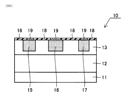
Figure 6 is a schematic diagram showing the state after performing a step
(S70) shown in the flowchart in Fig. 1 in Embodiment 1 of the present inven-
tion.
Figure 7 is a flowchart showing the method of producing the semiconductor
device in Embodiment 2 of the present invention.
Figure 8 is a schematic diagram showing the state after performing a step
(S80) shown in the flowchart in Fig. 7 in Embodiment 2 of the present inven-
tion.
Figure 9 is a flowchart showing the method of producing the semiconductor
device in Embodiment 3 of the present invention.
Figure 10 is a schematic diagram showing the state after performing a step
(S60) shown in the flowchart in Fig. 9 in Embodiment 3 of the present inven-
tion.
Figure 11 is a schematic diagram showing the state after performing a step
(S80) shown in the flowchart in Fig. 9 in Embodiment 3 of the present inven-
CA 02684876 2009-10-21
tion.
Figure 12 is a schematic diagram, for Embodiment 4 of the present inven-
tion, showing the state after performing a step (S10) and a step (S20) shown
in
the flowchart in Fig. 1.
Figure 13 is a schematic diagram, for Embodiment 4 of the present inven-
tion, showing the state after performing a step (S30) shown in the flowchart
in
Fig. 1.
Figure 14 is a schematic diagram, for Embodiment 4 of the present inven-
tion, showing the state after performing a step (S40) shown in the flowchart
in
Fig. 1.
Figure 15 is a schematic diagram, for Embodiment 4 of the present inven-
tion, showing the state after performing a step (S60) shown in the flowchart
in
Fig. 1.
Figure 16 is a schematic diagram, for Embodiment 1 of the present inven-
tion, showing the state after performing a step (S70) shown in the flowchart
in
Fig. 1.
Best Mode for Carrying Out the Invention
[0016)
Embodiments of the present invention are explained below by referring to
the drawing. In the individual embodiments, the same reference sign is given
to the member exercising the same function to eliminate a duplicated explana-
tion for that member unless particularly required.
CA 02684876 2009-10-21
11
[0017]
EMBODIMENT 1
Figure 1 is a flowchart showing the method of producing the semiconductor
device in Embodiment 1 of the present invention. Figure 2 is a schematic dia-
gram showing the state after performing a step (S10) and a step (S20) both
shown in the flowchart in Fig. 1 in Embodiment 1 of the present invention.
Figure 3 is a schematic diagram showing the state after performing a step
(S30) shown in the flowchart in Fig. 1 in Embodiment 1 of the present inven-
tion. Figure 4 is a schematic diagram showing the state after performing a
step (S40) shown in the flowchart in Fig. 1 in Embodiment 1 of the present in-
vention. Figure 5 is a schematic diagram showing the state after performing a
step (S60) shown in the flowchart in Fig. 1 in Embodiment 1 of the present in-
vention. Figure 6 is a schematic diagram showing the state after performing a
step (S70) shown in the flowchart in Fig. 1 in Embodiment 1 of the present in-
vention.
[00181
Embodiment 1 of the present invention shows the method of producing a
horizontal JFET 10 shown in Fig. 6 among semiconductor devices. As shown in
Fig. 6, the horizontal JFET 10 is a semiconductor device that is provided with
an n-type substrate 11, which has an n-type conduction type; a p-type semi-
conductor layer 12 formed on one main surface of the n-type substrate 11; an
n-type semiconductor layer 13 formed on the p-type semiconductor layer 12; a
source region 15 to which electrons are supplied; a drain region 17 from which
CA 02684876 2009-10-21
12
electrons are taken out; and a gate region 16, which is placed between the
source region 15 and the drain region 17 and which electrically connects or
disconnects between the source region 15 and the drain region 17. The semi-
conductor device is composed of, for example, SiC forming a hexagonal crystal.
It is desirable that the SiC be a polycrystalline type known as 4H-SiC.
[0019]
The n-type substrate 11, which constitutes a part of the JFET 10 in Em-
bodiment 1 of the present invention, which is composed of SiC, and which has
an n-type conduction type, is prepared so as to be in the direction at which
the
minimum angle between its main surface and a plane perpendicular to the
(0001) plane is one degree or less, for example, in the direction at which the
minimum angle between the main surface and the [0001] direction, which is
perpendicular to the (0001) plane, is one degree or less. The types of the
crys-
tal plane having a main surface in the direction along the [0001] direction in-
clude, for example, a plane equivalent to the (11-20) plane and a plane equiva-
lent to the (1-100) plane. Consequently, it is desirable to prepare the n-type
substrate 11 so as to form a minimum angle of one degree or less with respect
to, for example, a plane equivalent to the (11-20) plane. Alternatively, it is
de-
sirable to prepare the n-type substrate 11 so as to from a minimum angle of
one degree or less with respect to a plane equivalent to the (1-100) plane.
[0020]
The p-type semiconductor layer 12 is formed on the one main surface of the
n-type substrate 11 by epitaxial growth. The n-type semiconductor layer 13 is
CA 02684876 2009-10-21
13
formed on the p-type semiconductor layer 12 by the same method of epitaxial
growth. The reason for performing the epitaxial growth is to minimize the
floating capacitance of the semiconductor device. As shown in Fig. 6, the
source region 15 and the drain region 17 are formed separately with some dis-
tance in a region within a certain depth from the one main surface of the
n-type semiconductor layer 13, that is, in a surface layer. The gate region 16
is
formed in the surface layer existing between the source region 15 and the
drain region 17. The source region 15 and the drain region 17 are regions con-
taining a dopant that has an n-type conduction type (an n-type dopant) and
that has a concentration higher than that in the n-type semiconductor layer
13.
The gate region 16 is a region containing a dopant that has a p-type conduc-
tion type (a p-type dopant) and that has a concentration higher than that in
the p-type semiconductor layer 12. The JFET 10 may have a configuration in-
verted from the above-described configuration with respect to the conduction
type (a p-type and n-type) of the semiconductor. In other words, the JFET 10
may have a structure in which an n-type semiconductor layer and a p-type
semiconductor layer are successively formed on one main surface of a p-type
substrate that is composed of p-type SiC and that has a p-type conduction
type.
(0021)
An ohmic electrode 19 is formed so as to be in contact with the top surface of
each of the source region 15, the gate region 16, and the drain region 17. The
ohmic electrode 19 is formed of material that can achieve ohmic contact with
CA 02684876 2009-10-21
14
the source region 15, the gate region 16, and the drain region 17, such as
nickel silicide (NiSi).
[0022]
An oxide film 18 is formed between the neighboring ohmic electrodes 19.
More specifically, the oxide films 18 as insulating layers are formed on the
top
surface of the n-type semiconductor layer 13 so as to cover the entire region
other than the regions in which the ohmic electrodes 19 are formed. Thus, the
neighboring ohmic electrodes 19 are insulated from each other.
[0023]
Next, an explanation is given to the method of producing the semiconductor
device in Embodiment 1 of the present invention by referring to Figs. 1 to 6.
In
the method of producing the JFET 10, which is the semiconductor device in
Embodiment 1 of the present invention, first, as shown in Fig. 1, a sub-
strate-preparing step (S10) is performed. More specifically, as described
above,
the n-type substrate 11 (see Figs. 2 to 6), which has an n-type conduction
type
and which is composed of SiC whose crystal is a hexagonal crystal, is prepared
so as to be in the direction at which the minimum angle between its main sur-
face and a plane perpendicular to the (0001) plane is one degree or less, for
example, in the direction at which the minimum angle between the main sur-
face and, for example, the [0001] direction, which is perpendicular to the
(0001) plane, is one degree or less. The types of the crystal plane having a
main surface in the direction along the [0001] direction include, for example,
a
plane equivalent to the (11-20) plane and a plane equivalent to the (1-100)
CA 02684876 2009-10-21
plane. Consequently, it is desirable to prepare the n-type substrate 11 so as
to
form a minimum angle of one degree or less with respect to, for example, a
plane equivalent to the (11-20) plane. Alternatively, it is desirable to
prepare
the n-type substrate 11 so as to form a minimum angle of one degree or less
with respect to a plane equivalent to the (1-100) plane.
[0024]
Next, as shown in Fig. 1, an epitaxial growth step (S20) is performed. More
specifically, as shown in Fig. 2, in this step, the p-type semiconductor layer
12
and the n-type semiconductor layer 13 both composed of SiC are successively
formed in lamination through, for example, vapor phase epitaxial growth on
one main surface of the n-type substrate 11 prepared in the previous step
(S10).
Electric current flows in the n-type semiconductor layer 13. To control the
path
of the current (to suppress the width of the current path from excessively
broadening), the p-type semiconductor layer 12 is placed. In the vapor phase
epitaxial growth, for example, a silane (SiH4) gas and a propane (C3H8) gas
may be used as the material gas and a hydrogen (H2) gas may be used as the
carrier gas. As the p-type dopant source for forming the p-type semiconductor
layer 12, for example, diborane (B2H6) or trimethylaluminum (TMA) may be
used. As the n-type dopant source for forming the n-type semiconductor layer
13, for example, a nitrogen (N2) gas may be used.
[0025]
Next, as shown in Fig. 1, a first ion implantation step (S30) is performed.
More specifically, in this step, the source region and the drain region both
CA 02684876 2009-10-21
16
containing a high-concentration n-type dopant are formed. By referring to Fig.
3, first, photoresist is applied onto a top surface 13A of the n-type
semiconduc-
tor layer 13. Then, exposure to light and development are performed to form a
resist film having openings at areas according to the shape of the source
region
15 and drain region 17. By using the resist film as a mask, an n-type dopant,
such as phosphorus (P), is introduced into the n-type semiconductor layer 13
through the ion implantation. In place of P, nitrogen (N) may be ion-
implanted.
Furthermore, in place of the ion implantation, an n-type epitaxial layer may
be grown as a buried layer to perform a step as the first ion implantation
step
(S30). Thus, the source region 15 and the drain region 17 are formed.
[00261
Next, a second ion implantation step (S40) is performed. In this step (S40),
the gate region containing a high-concentration p-type dopant is formed. More
specifically, by referring to Fig. 4, first, as with the procedure used in the
step
(S30), a resist film is formed that has an opening at an area according to the
shape of the gate region 16. By using the resist film as a mask, a p-type
dopant,
such as aluminum (Al), is introduced into the n-type semiconductor layer 13
through ion implantation. In place of Al, boron (B) may be ion-implanted.
Furthermore, in place of the ion implantation, a p-type epitaxial layer may be
grown as a buried layer to perform a step as the second ion implantation step
(S40). Thus, the gate region 16 is formed. The present invention does not
strictly specify the order of performing the above-described first ion
implanta-
tion step (S30) and second ion implantation step (S40). In other words, the
two
CA 02684876 2009-10-21
17
steps may be performed with the reversed order.
[0027]
Next, an activation annealing step (S50) is performed. In this step (S50),
first, the resist film formed in the step (S40) is removed. Then, the n-type
semiconductor layer 13, which has undergone the ion implantation in the steps
(S30) and (S40), is heated to activate the dopants introduced by the
above-described ion implantation. Thus, activation annealing is performed by
conducting a heat treatment. The activation annealing may be performed by
conducting the heat treatment in, for example, an argon (Ar) gas atmosphere.
The activation annealing may also be performed by conducting the heat
treatment in an inert-gas atmosphere, such as a neon (Ne) gas atmosphere, in
place of the Ar gas atmosphere. Furthermore, the activation annealing may
also be performed by conducting the heat treatment in a vacuum.
[0028)
Next, an oxide-film-forming step (S60) is performed. By referring to Fig. 5,
this step (S60) performs the heat oxidation of the n-type semiconductor layer
13, which includes the ion-implanted layers formed through the steps (S10) to
(S50), the p-type semiconductor layer 12, and the n-type substrate 11. Thus,
an oxide film 18 composed of silicon dioxide (Si02) is formed as a field oxide
film so as to cover the top surface 13A of the n-type semiconductor layer 13.
[0029]
Next, an ohmic-electrode-forming step (S70) is performed. As shown in Fig. 6,
in this step (S70), an ohmic electrode 19 composed of, for example, NiSi is
CA 02684876 2009-10-21
18
formed so as to be in contact with the top surface of each of the source
region
15, the gate region 16, and the drain region 17. More specifically, first, by
the
same procedure as used in the step (S30), a resist film is formed that has
openings at areas according to the shapes of the ohmic electrodes 19. By using
the resist film as a mask, the oxide film 18 (the field oxide film) on the
source
region 15, the gate region 16, and the drain region 17 is removed by, for exam-
ple, reactive ion etching (RIE).
[00301
Subsequently, by vapor-depositing, for example, Ni, an Ni layer is formed on
the source region 15, the gate region 16, and the drain region 17, all of
which
are exposed at the openings of the oxide film 18 before the Ni layer is
formed,
and on the resist film as well. Then, by removing the resist film, the Ni
layer
on the resist film is removed (the liftoff method). As a result, the Ni layer
re-
mains on the source region 15, the gate region 16, and the drain region 17,
all
of which were exposed at the openings of the oxide film 18 before the Ni layer
was formed. Next, heat treatment is performed by heating them at about
950 C for about two minutes in, for example, an argon (Ar) atmosphere. The
heat treatment performs silicidation of the Ni layer. Thus, as shown in Fig.
6,
the ohmic electrodes 19 are formed that are composed of NiSi and that can
form ohmic contact with the source region 15, the gate region 16, and the
drain
region 17.
[00311
In addition to the above-described liftoff method, the ohmic electrode can be
CA 02684876 2009-10-21
19
formed by another method, which etching-removes unnecessary portions in the
film through the photolithographic technique after the film is formed on the
entire surface. More specifically, as in the above-described oh-
mic-electrode-forming step (S70), first, the oxide film 18 (the field oxide
film)
on the source region 15, the gate region 16, and the drain region 17 is
removed.
Then, by vapor-depositing, for example, Ni, an Ni layer is formed. Subse-
quently, photoresist is applied onto the top surface of the formed Ni layer.
Next,
exposure to light and development are performed to form a resist film having
openings at areas other than the areas for the source region 15, gate region
16,
and drain region 17. By using the resist film as a mask, the Ni layer is re-
moved at the areas where no Ni layer is required (the areas other than the
areas on the source region 15, the gate region 16, and the drain region 17)
through, for example, wet etching. As a result, the Ni layer remains on the
source region 15, gate region 16, and drain region 17. After that, as with the
above-described procedure, heat treatment is performed by heating them at
about 950 C for about two minutes in, for example, an Ar atmosphere. The
heat treatment performs silicidation of the Ni layer. Thus, as shown in Fig.
6,
the ohmic electrodes 19 are formed that are composed of NiSi and that can
form ohmic contact with the source region 15, the gate region 16, and the
drain
region 17.
[0032]
In Embodiment 1 of the present invention, as described above, the JFET 10
may have a configuration inverted from the above-described configuration
~ CA 02684876 2009-10-21
with respect to the conduction type (a p-type and n-type) of the
semiconductor.
In the case where the inverted configuration is employed, when the ohmic
electrodes 19 are to be formed on the top surface of the p-type semiconductor
layer 12, the ohmic electrodes may be formed by using alloy composed of tita-
nium (Ti) and Al, which is TiAl. More specifically, a Ti layer and an Al layer
are successively formed on the source region 15, the gate region 16, and the
drain region 17 using, for example, the above-described liftoff method or
photolithographic technique. After that, as with the above-described
procedure,
heat treatment is performed by heating them at about 950 C for about two
minutes in, for example, an Ar atmosphere. The heat treatment forms the oh-
mic electrodes 19 that are composed of TiAI and that can form ohmic contact
with the source region 15, the gate region 16, and the drain region 17.
[0033)
The JFET 10 formed through the above-described steps uses a depletion
layer formed in the reverse-biased p-n junction to vary the cross-sectional
area
of the region through which the electric current flows. Thus, the current flow-
ing between the source region 15 and the drain region 17 is controlled. In
other words, this structure directs the current to flow between the source re-
gion 15 and the drain region 17, that is, to flow in the direction along the
main
surface of the n-type substrate 11. Therefore, this structure has a horizontal
structure. Consequently, as shown in Embodiment 1 of the present invention,
the n-type substrate 11 is prepared so as to be in the direction at which the
minimum angle between its main surface and a plane perpendicular to the
CA 02684876 2009-10-21
21
(0001) plane is one degree or less, for example, in the direction at which the
minimum angle between the main surface and, for example, the [0001] direc-
tion, which is perpendicular to the (0001) plane, is one degree or less. As a
re-
sult, in comparison with, for example, the case where the preparation is per-
formed in such a way that the main surface is in the direction along the
(0001)
plane, the values of the insulation breakdown electric field, breakdown
voltage,
and electron mobility can be increased and the value of the on-resistance can
be decreased.
[0034]
EMBODIMENT 2
Figure 7 is a flowchart showing the method of producing the semiconductor
device in Embodiment 2 of the present invention. Figure 8 is a schematic dia-
gram showing the state after performing a step (S80) shown in the flowchart
in Fig. 7 in Embodiment 2 of the present invention.
[0035]
Embodiment 2 of the present invention shows the method of producing a
horizontal MOSFET 20 shown in Fig. 8 among semiconductor devices. As
shown in Fig. 8, in the horizontal MOSFET 20, an ohmic electrode 19 is
formed so as to be in contact with the top surface of each of the source
region
15 and the drain region 17. In the top surface 13A of the n-type semiconductor
layer 13 (see Figs. 2 to 5), an oxide film 18 is formed on the top surface of
the
gate region 16 as with the areas other than the areas on the top surface of
the
source region 15 and the drain region 17. Of the oxide films 18, in
particular,
CA 02684876 2009-10-21
22
the oxide film 18 formed on the top surface of the gate region 16 is used as a
gate oxide film. A gate electrode 21 is formed on the top surface of that
oxide
film 18 (the gate oxide film). The horizontal MOSFET 20 is different from the
horizontal JFET 10 in Embodiment 1 of the present invention only in the
above-described features.
[0036)
As shown in Figs. 7 and 8, the method of producing the horizontal MOSFET
20 in Embodiment 2 of the present invention is the same as that of the hori-
zontal JFET 10 in Embodiment 1 of the present invention in the steps from
the substrate-preparing step (S10) to the activation annealing step (S50).
Nevertheless, as shown in Fig. 8, in the second ion implantation step (S40),
the gate region 16 is formed so as to pass through the n-type semiconductor
layer 13 and penetrate into the p-type semiconductor layer 12 to a certain
depth. This structure interconnects the gate region 16 with the p-type semi-
conductor layer 12. As a result, the operation of the MOSFET 20 by the inver-
sion of the gate region 16 can be performed smoothly. In this case, it is
desir-
able that the concentration of the p-type dopant to be implanted into the gate
region 16 be comparable to that of the p-type dopant contained in the p-type
semiconductor layer 12 and be adjusted so as to fall within an error range of
10%.
[0037)
In the next oxide-film-forming step (S60), the oxide film 18 is formed at the
gate region 16's top surface in the n-type semiconductor layer 13's top
surface
CA 02684876 2009-10-21
~' .
23
13A (see Figs. 2 to 5). The oxide film 18 is an oxide film for creating the
field
effect of the MOS structure. Consequently, in comparison with the previously
described oxide film 18 (the field oxide film) formed in the oxide-film-
forming
step (S60) in Embodiment 1 of the present invention, the oxide film 18 (the
gate oxide film) having a desired thickness can be formed by performing a heat
oxidation for a shorter time. In this case, the thickness of the oxide films
18
formed in the area other than both the area at which the gate oxide film,
which is the oxide film 18 on the gate region 16, is formed and the area at
which ohmic electrodes are to be formed in the next step (S70) is thinner than
the thickness of, for example, the previously described oxide film 18 (the
field
oxide film) formed in Embodiment 1 of the present invention. After the forma-
tion of the above-described oxide film 18 (the gate oxide film), in the top
sur-
face 13A of the n-type semiconductor layer 13, the formation of the oxide film
may be further continued only in the area other than both the area at which
the gate oxide film is formed and the area at which ohmic electrodes are to be
formed in the next step (S70), for example. When this operation is imple-
mented, a field oxide film thicker than the gate oxide film can be formed.
[00381
Next, the ohmic-electrode-forming step (S70) is performed. More specifically,
as shown in Fig. 8, an ohmic electrode 19 composed of, for example, NiSi is
formed so as to be in contact with the top surface of each of the source
region
15 and the drain region 17. In the case where the inverted configuration is
employed as described earlier, when the ohmic electrodes 19 are to be formed
CA 02684876 2009-10-21
,
ti
24
on the top surface of the p-type semiconductor layer, the ohmic electrodes may
be formed by using alloy composed of titanium (Ti) and Al, which is TiAl.
[0039]
Next, a gate-electrode-forming step (S80) is performed. More specifically, as
shown in Fig. 8, a gate electrode 21 formed of, for example, an Al layer is
formed so as to be in contact with the top surface of the oxide film 18 (the
gate
oxide film) formed, in the above-described oxide-film-forming step (S60), on
the
top surface of the gate region 16. More specifically, for example, after the
oh-
mic-electrode-forming step (S70) is performed, for example, Al is va-
por-deposited on the entire top surface of both the oxide films 18 and the oh-
mic electrodes 19 to form an Al layer. Subsequently, photoresist is applied
onto
the top surface of the formed Al layer. Then, exposure to light and
development
are performed to form a resist film having openings at areas other than the
area on the top surface of the oxide film 18 (the gate oxide film) formed on
the
top surface of the gate region 16. By using the resist film as a mask, the Al
layer is removed at the areas where no Al layer is required (the areas other
than the area on the top surface of the oxide film 18 (the gate oxide film)
formed on the top surface of the gate region 16) through, for example, wet
etching. As a result, the Al layer remains on the top surface of the oxide
film
18 (the gate oxide film) formed on the top surface of the gate region 16. The
above-described operation forms the Al layer as the gate electrode 21 at the
desired location.
[00401
CA 02684876 2009-10-21
In place of the above-described Al, the gate electrode 21 may be formed by
using polycrystalline silicon. In this case, the gate electrode is formed
through
the same method as used in the case of the above-described Al. In addition to
the above-described method, the gate electrode 21 may be formed by using, for
example, the liftoff method.
[0041]
In the MOSFET 20 formed through the above-described steps, a channel
layer is formed in the surface layer existing between the source region 15 and
the drain region 17 in the n-type semiconductor layer 13. The MOSFET 20
controls the value of the current flowing between the source region 15 and the
drain region 17 by changing the state of the channel layer in the surface
layer
(especially in the vicinity of the gate region 16) according to the magnitude
of
the voltage applied to the gate electrode 21. In other words, this structure
di-
rects the current to flow between the source region 15 and the drain region
17,
that is, to flow in the direction along the main surface of the n-type
substrate
11. Therefore, this structure has a horizontal structure. Consequently, as
shown in Embodiment 2 of the present invention, the n-type substrate 11 is
prepared so as to be in the direction at which the minimum angle between its
main surface and a plane perpendicular to the (0001) plane is one degree or
less, for example, in the direction at which the minimum angle between the
main surface and the [0001] direction, which is perpendicular to the (0001)
plane, is one degree or less. As a result, in comparison with, for example,
the
case where the preparation is performed in such a way that the main surface
CA 02684876 2009-10-21
26
is in the direction along the (0001) plane, the values of the insulation break-
down electric field, breakdown voltage, and electron mobility can be increased
and the value of the on-resistance can be decreased, as described before.
[0042]
Embodiment 2 is different from Embodiment 1 of the present invention only
in the above-described features. More specifically, the structure, conditions,
production steps, and so on all not described in the explanation of Embodiment
2 of the present invention are in conformance with those of Embodiment 1 of
the present invention.
[0043]
EMBODIMENT 3
Figure 9 is a flowchart showing the method of producing the semiconductor
device in Embodiment 3 of the present invention. Figure 10 is a schematic
diagram showing the state after performing the step (S60) shown in the flow-
chart in Fig. 9 in Embodiment 3 of the present invention. Figure 11 is a sche-
matic diagram showing the state after performing the step (S80) shown in the
flowchart in Fig. 9 in Embodiment 3 of the present invention.
[0044]
Embodiment 3 of the present invention shows the method of producing a
horizontal MESFET 30 shown in Fig. 11 among semiconductor devices. As
shown in Fig. 11, in the horizontal MESFET 30, an ohmic electrode 19 is
formed so as to be in contact with the top surface of each of the source
region
15 and the drain region 17. The gate region 16 provided in, for example, the
CA 02684876 2009-10-21
27
JFET 10 shown in Fig. 6 and the MOSFET 20 shown in Fig. 8 is not provided
in the MESFET 30. Instead, a gate electrode 22 that is in Schottky contact
with the n-type semiconductor layer 13 is directly placed on the top surface
13A of the n-type semiconductor layer 13. More specifically, the gate
electrode
22 is placed on the top surface of the region where the gate region 16 is pro-
vided in the JFET 10 and the MOSFET 20. The horizontal MESFET 30 is dif-
ferent from the horizontal JFET 10 in Embodiment 1 of the present invention
only in the above-described feature.
[0045]
As shown in Figs. 7 and 8, the method of producing the horizontal MESFET
30 in Embodiment 3 of the present invention is the same as that of the hori-
zontal JFET 10 in Embodiment 1 of the present invention in the steps from
the substrate-preparing step (S10) to the first ion implantation step (S30).
Nevertheless, as described above, because the gate region 16 is not formed,
the
second ion implantation is not performed. Therefore, the next step is the acti-
vation annealing step (S50). The activation annealing step (S50) and the ox-
ide-film-forming step (S60) are the same as those of the previously described
horizontal JFET 10 in Embodiment 1 of the present invention.
[00461
Next, the ohmic-electrode-forming step (S70) is performed. More specifically,
as shown in Fig. 11, an ohmic electrode 19 composed of, for example, NiSi is
formed so as to be in contact with the top surface of each of the source
region
15 and the drain region 17. In the case where the inverted configuration is
CA 02684876 2009-10-21
28
employed as described earlier, when the ohmic electrodes 19 are to be formed
on the top surface of the p-type semiconductor layer, the ohmic electrodes may
be formed by using alloy composed of titanium (Ti) and Al, which is TiAl.
[0047]
Next, the gate-electrode-forming step (S80) is performed. More specifically,
in this step, for example, the gate electrode 22 is formed on the n-type semi-
conductor layer 13's surface existing between the source region 15 and the
drain region 17 (in the top surface 13A of the n-type semiconductor layer 13,
the top surface of the region where the gate region 16 is provided in the JFET
and the MOSFET 20). More specifically, for example, after the oh-
mic-electrode-forming step (S70) is performed, photoresist is applied onto the
entire top surface of the oxide films 18 and the ohmic electrodes 19. Then, ex-
posure to light and development are performed to form a resist film having an
opening at the area according to the shape of the oxide film 18 at the area
where the gate electrode 22 is to be formed. In other words, in the top
surface
13A of the n-type semiconductor layer 13, the opening is located at the top
surface of the region where the gate region 16 is provided in the JFET 10 and
the MOSFET 20. By using the resist film as a mask, a metallic material that
can be in Schottky contact with the n-type semiconductor layer 13, such as Ni,
is vapor-deposited. Thus, an Ni layer is formed on the top surface of the ex-
posed n-type semiconductor layer 13 without being covered by the oxide film
18 (the exposed portion is the area where the gate electrode 22 is to be
formed)
and on the resist film on the top surface of the oxide films 18 and the ohmic
CA 02684876 2009-10-21
, ~ .
29
electrodes 19. Then, by removing the resist film, the Ni layer on the resist
film
is removed (the liftoff method). As a result, the Ni layer remains on the once
exposed n-type semiconductor layer 13 without being covered by the oxide film
18. Thus, the Ni layer as the gate electrode 22 is formed at the desired loca-
tion.
[0048]
In the case where the inverted configuration is employed as described earlier,
when the gate electrode 22 is to be formed on the top surface of the p-type
semiconductor layer, the gate electrode 22 may be formed by using Ti in place
of the above-described Ni and by using the same method as used in the case of
the above-described Ni. In addition to the above-described method, the gate
electrode 22 may be formed by using an any method that properly combines,
for example, the above-described liftoff method and the photolithographic
technique.
[0049]
The MESFET 30 formed through the above-described steps differs from the
earlier-described JFET 10 in that, for example, in place of the p-n junction
used in the gate region of the JFET 10, a Schottky contact between a metal
and a semiconductor (between the gate electrode 22 and the n-type semicon-
ductor layer 13) is used. Nevertheless, the MESFET 30 performs the operation
basically similar to that of the JFET 10. More specifically, the MESFET 30
controls the current flowing between the source region 15 and the drain region
17. In other words, this structure directs the current to flow between the
CA 02684876 2009-10-21
source region 15 and the drain region 17, that is, to flow in the direction
along
the main surface of the n-type substrate 11. Therefore, the MESFET 30 has a
horizontal structure. Consequently, as shown in Embodiment 3 of the present
invention, the n-type substrate 11 is prepared so as to be in the direction at
which the minimum angle between its main surface and a plane perpendicular
to the (0001) plane is one degree or less, for example, in the direction at
which
the minimum angle between the main surface and the [0001] direction, which
is perpendicular to the (0001) plane, is one degree or less. As a result, in
com-
parison with the case where the preparation is performed in such a way that
the main surface is in the direction along the (0001) plane, the values of the
insulation breakdown electric field, breakdown voltage, and electron mobility
can be increased and the value of the on-resistance can be decreased, as de-
scribed before.
[0050]
Embodiment 3 is different from Embodiment 1 of the present invention only
in the above-described features. More specifically, the structure, conditions,
production steps, and so on all not described in the explanation of Embodiment
3 of the present invention are in conformance with those of Embodiment 1 of
the present invention.
[0051]
EMBODIMENT 4
Figure 12 is a schematic diagram, for Embodiment 4 of the present inven-
tion, showing the state after performing a step (S10) and a step (S20) shown
in
CA 02684876 2009-10-21
31
the flowchart in Fig. 1. Figure 13 is a schematic diagram, for Embodiment 4 of
the present invention, showing the state after performing a step (S30) shown
in the flowchart in Fig. 1. Figure 14 is a schematic diagram, for Embodiment 4
of the present invention, showing the state after performing a step (S40)
shown in the flowchart in Fig. 1. Figure 15 is a schematic diagram, for Em-
bodiment 4 of the present invention, showing the state after performing a step
(S60) shown in the flowchart in Fig. 1. Figure 16 is a schematic diagram, for
Embodiment 1 of the present invention; showing the state after performing a
step (S70) shown in the flowchart in Fig. 1.
[0052]
Embodiment 4 of the present invention shows the method of producing a
horizontal RESURF-JFET 40 shown in Fig. 16 among semiconductor devices.
As shown in Fig. 16, in the horizontal RESURF-JFET 40, a thin second p-type
semiconductor layer 14 is further formed on the n-type semiconductor layer 13
through epitaxial growth. The source region 15, the gate region 16, and the
drain region 17 are formed so as to pass through the second p-type semicon-
ductor layer 14 and penetrate into the n-type semiconductor layer 13 to a cer-
tain depth from one main surface of the second p-type semiconductor layer 14
(see Figs. 14 to 16). This structure enables the achievement of a uniform dis-
tribution of the electric-field strength in the region between the gate region
16
and the drain region 17 and therefore the suppression of the field concentra-
tion. The presence of the second p-type semiconductor layer 14 enables the
reduction of the parasitic resistance at the inside of the semiconductor
device.
CA 02684876 2009-10-21
32
The horizontal RESURF-JFET 40 is different from the horizontal JFET 10 in
Embodiment 1 of the present invention only in the above-described features.
[0053]
In the method of producing the horizontal RESURF-JFET 40 in Embodi-
ment 4 of the present invention, in the epitaxial growth step (S20), after the
formation of the n-type semiconductor layer 13, the second p-type semicon-
ductor layer 14 is formed on the n-type semiconductor layer 13 through epi-
taxial growth. In the first ion implantation step (S30) and the second ion im-
plantation step (S40), resist application, exposure to light, and development
are performed so as to form the source region 15, the gate region 16, and the
drain region 17 in such a way that they pass through the second p-type semi-
conductor layer 14 and penetrate into the n-type semiconductor layer 13 to a
certain depth from the one main surface of the second p-type semiconductor
layer 14. In the oxide-film-forming step (S60), an oxide film 18 composed of
silicon dioxide (Si02) is formed as a field oxide film so as to cover the top
sur-
face 14A of the second p-type semiconductor layer 14. The method of producing
the RESURF-JFET 40 is different from the previously described method of
producing the JFET 10 in Embodiment 1 of the present invention only in the
above-described features.
[0054]
Embodiment 4 is different from Embodiment 1 of the present invention only
in the above-described features. More specifically, the structure, conditions,
production steps, and so on all not described in the explanation of Embodiment
CA 02684876 2009-10-21
33
4 of the present invention are in conformance with those of Embodiment 1 of
the present invention.
Example 1
[0055]
In the following, the present invention is explained further concretely by re-
ferring to Examples. Nevertheless, the present invention is not limited by
these Examples.
[0056]
In the following individual Examples, the evaluation is conducted by pro-
ducing the previously described JFET 10 in Embodiment 1 of the present in-
vention. Consequently, the explanation is given by referring to Figs. 1 to 6
as
needed.
[0057]
The method of forming the JFET 10 as Example 1 is explained below. First,
the substrate-preparing step (S10) shown in Fig. 1 is performed. The substrate
is a semiconductor having a hexagonal crystal. An SiC wafer as the substrate
is prepared so as to be in the direction at which the minimum angle between
its main surface and a plane perpendicular to the (0001) plane is one degree
or
less, for example, in the direction at which the minimum angle between the
main surface and, for example, the [0001] direction, which is perpendicular to
the (0001) plane, is one degree or less. It is desirable that the SiC be a
poly-
crystalline type known as 4H-SiC. An SiC wafer is prepared that has an n-type
CA 02684876 2009-10-21
34
conduction type and that has a main surface formed of a plane equivalent to
the (11-20) plane as the crystal plane having a main surface that is in the di-
rection at which the minimum angle between the main surface and the [0001]
direction is one degree or less (the wafer corresponds to the n-type substrate
11 in Figs. 2 to 6). In the epitaxial growth step (S20) shown in Fig. 1, on
one
main surface of the n-type semiconductor layer 11, a p-type semiconductor
layer 12 having a thickness of 10 m and a p-type dopant concentration of 1
X 1016 cm-3 and an n-type semiconductor layer 13 having a thickness of 0.7 u
m and an n-type dopant concentration of 1 X 1017 cm-3 are successively
formed through epitaxial growth.
[0058]
Next, in the first ion implantation step (S30) shown in Fig. 1, the ion im-
plantation of P is performed to form a source region 15 and a drain region 17
both having a depth of 0.5 m from the surface of the n-type semiconductor
layer 13 and a dopant concentration of 5 X 1018 cm-3. In the second ion im-
plantation step (S40) shown in Fig. 1, the ion implantation of Al is performed
to form a gate region 16 having a depth of 0.4 ,u m from the surface of the
n-type semiconductor layer 13 and a dopant concentration of 2 X 1018 cm-3.
[0059]
Next, in the activation annealing step (S50) shown in Fig. 1, the SiC wafer
under the process of forming the JFET 10 is heated at 1,700 C for 30 minutes
in an Ar gas atmosphere. In the oxide-film-forming step (S60) shown in Fig. 1,
the SiC wafer under the process of forming the JFET 10 is heated at 1,300 C
CA 02684876 2009-10-21
for 60 minutes in an oxygen gas atmosphere to form an oxide film 18 as a field
oxide film. In the ohmic-electrode-forming step (S70), first, the oxide film
18
(the field oxide film) on the source region 15, the gate region 16, and the
drain
region 17 is removed. Then, by vapor-depositing, for example, Ni, an Ni layer
as the ohmic electrode 19 is formed on the top surface of the source region
15,
the gate region 16, and the drain region 17. Through the above-described pro-
cedure, the JFET 10 as Example 1 of the present invention is formed.
Example 2
[0060]
The method of forming the JFET 10 as Example 2 is explained below. First,
the substrate-preparing step (S10) shown in Fig. 1 is performed. The substrate
is a semiconductor having a hexagonal crystal. An SiC wafer as the substrate
is prepared so as to be in the direction at which the minimum angle between
its main surface and a plane perpendicular to the (0001) plane is one degree
or
less, for example, in the direction at which the minimum angle between the
main surface and, for example, the [0001] direction, which is perpendicular to
the (0001) plane, is one degree or less. In the method of forming the JFET 10
as Example 2, an SiC wafer is prepared that has an n-type conduction type
and that has a main surface formed of a plane equivalent to the (1-100) plane
as the crystal plane having a main surface that is in the direction at which
the
minimum angle between the main surface and the [0001] direction is one de-
gree or less (the wafer corresponds to the n-type substrate 11 in Figs. 2 to
6).
CA 02684876 2009-10-21
36
The JFET 10 as Example 2 is different from the JFET 10 as Example 1 only in
the above-described features. More specifically, the structure, conditions,
pro-
duction steps, and so on all not described in the explanation of the method of
forming the JFET 10 as Example 2 are in conformance with those of the
method of forming the JFET 10 as Example 1.
[0061]
COMPARATIVE EXAMPLE
An explanation is given below to the method of forming a JFET as Com-
parative example in comparison with the above-described JFETs 10 as Exam-
ples 1 and 2 formed in accordance with Embodiment 1 of the present invention.
First, the substrate-preparing step (S10) shown in Fig. 1 is performed. The
JFET as Comparative example includes a semiconductor material having a
hexagonal crystal. An SiC wafer as the substrate (see the n-type substrate 11
in Figs. 2 to 6) is prepared so as to be in the direction at which the minimum
angle between its main surface and a direction parallel to the (0001) plane is
eight degrees. The JFET as Comparative example is different from the JFET
as Example 1 only in the above-described feature. More specifically, the
structure, conditions, production steps, and so on all not described in the ex-
planation of the method of forming the JFET as Comparative example are in
conformance with those of the method of forming the JFET 10 as Example 1.
[0062]
As described above, the following JFETs were formed under all other condi-
tions are same:
CA 02684876 2009-10-21
37
(a) the JFETs 10 as Examples 1 and 2 each having a substrate formed so as to
have a crystal plane in accordance with the embodiment of the present inven-
tion, and
(b) the JFET as Comparative example in which the substrate's main surface is
in the direction along the (0001) plane in accordance with the conventional
practice.
The individual JFETs were subjected to measurements of the breakdown volt-
age and the on-resistance. In the above description, the breakdown voltage is
the maximum voltage that can be applied between the ohmic electrode on the
source region and the ohmic electrode on the drain region and is expressed in
the unit volt (V). The on-resistance is the electrical resistance between the
ohmic electrode on the source region and the ohmic electrode on the drain re-
gion during the time of the on-state in which the JFET is driven by causing a
current to flow between the source region and the drain region through the
application of a voltage to the ohmic electrode on the gate region. Table I
below shows the results of the measurements.
[0063]
Table I
Breakdown volt- Ratio of break- Ratio of
age (V) down voltage on-resistance
Example 1 275 1.62 0.83
Example 2 280 1.65 0.85
Comparative 170 1 1
example
[00641
CA 02684876 2009-10-21
38
As can be seen from the results shown in Table I , both of Examples 1 and 2
improve the magnitude of the breakdown voltage over Comparative example
by more than 100 V. When the magnitude of breakdown voltage of Compara-
tive example is taken as 1, both of Examples 1 and 2 have a magnitude of
breakdown voltage of more than 1.6. When the magnitude of on-resistance of
Comparative example is taken as 1, the on-resistance of Example 1 is 0.83 and
that of Example 2 is 0.85. This result shows that the on-resistance is also
sig-
nificantly improved. The above results show that because the horizontal semi-
conductor device is formed such that the SiC substrate is in the direction in-
tersecting the (0001) plane, the value of breakdown voltage is increased and
the value of on-resistance is decreased in comparison with the conventional
case where the semiconductor device is formed such that the SiC substrate is
in the direction along the (0001) plane. As described above, by forming a hori-
zontal semiconductor device such that its SiC substrate is in the direction in-
tersecting the (0001) plane, for example, in the direction at which the mini-
mum angle between its main surface and a plane perpendicular to the (0001)
plane is one degree or less, the values of the insulation breakdown electric
field, breakdown voltage, and on-resistance can be considerably improved. In a
horizontal semiconductor device, a current flows in the direction along the
main surface of the substrate, showing that an electric field is applied. The
values of the breakdown voltage and the electron mobility in the direction
along the main surface of the substrate can be increased. Consequently, it is
likely that when a semiconductor device is formed in such a way that the SiC
CA 02684876 2009-10-21
39
substrate is in the direction intersecting the (0001) plane, for example, in
the
direction at which the minimum angle between its main surface and a plane
perpendicular to the (0001) plane is one degree or less, even the allowable
value of the current can be increased, for example.
[0065]
It is to be considered that the above-disclosed embodiments and examples
are illustrative and not restrictive in all respects. The scope of the present
in-
vention is shown by the scope of the appended claims, not by the
above-described embodiments. Accordingly, the present invention is intended
to cover all revisions and modifications included within the meaning and scope
equivalent to the scope of the claims.
Industrial Applicability
[0066]
The method of the present invention for producing a semiconductor device is
excellent as a technique for improving the breakdown voltage and the
on-resistance.