Note: Descriptions are shown in the official language in which they were submitted.
CA 02685191 2009-10-26
WO 2008/135753
PCT/GB2008/001553
- 1 -
Multiport Amplifiers in Communications Satellites
Technical Field
This invention relates to multiport amplifiers for use within a satellite
communication system, and specifically to a method and apparatus for
maintaining isolation within multiport amplifiers..
Background Art
Interest continues to grow in the application of Multiport Amplifiers (MPAs)
to
Ku and Ka-band satellite payloads - See for example, A Couchman, D. Jones,
"Optimized Multiport Amplifiers for Wideband Multi-beam Satellites", AIAA,
24th
o International Communications Satellite Systems Conference, San Diego,
USA,
June 2006; A. Anakabe, et al, "Ka-band Multi-port Amplifier Characteristics
for
Space Telecommunication Operation", 6th International Vacuum Electronics
Conference, Noordwijk, Netherlands, April, 2005.
MPAs are particularly applicable to Single Feed per Beam (SFB)
architectures which generate a set of regular contiguous beams over a defined
coverage region, using a system of typically 4 antenna reflectors with
associated feedhorns . The beam set employs a high degree of frequency re-
use, with each beam generated uniquely by a corresponding feed horn. Such
architectures are comparatively highly efficient in terms of RF power
generation.
However, they are much restricted in the flexibility with which they can
distribute
this power over the coverage area. The application of MPAs, with each
feedhorn driven by a respective MPA output, would greatly increase the
flexibility of the SFB design, significantly enhancing the flexibility of this
architecture by enabling capacity (transmitted power) to follow dynamically
changes in traffic distribution over the coverage zone. MPAs could be used in
wideband, selectable bandwidth transponders providing flexible allocation of
power as well as bandwidth to all beams ensuring optimum link parameters in
each case.
An MPA is a well-known power amplifier device used for satellite
communications, which operates at the microwave frequency bands. An MPA
includes a number N of similar amplifier units (TWT or solid state) in
parallel,
CA 02685191 2009-10-26
WO 2008/135753
PCT/GB2008/001553
- 2 -
each having a power P, so that each input signal is amplified equally by each
amplifier, to increase the power of each output signal by a factor N, to PxN.
N
input ports and N output ports are provided, so that an input signal on one
input
port is routed to the corresponding output port. The input ports are connected
6 to the amplifier units by a low power input network (INET) that may be
implemented in any convenient transmission line technology that is appropriate
to the circumstances, e.g. microstrip, stripline, coaxial cable, or waveguide.
The
output ports are connected to the amplifier units by a high power output
network
(ONET) that is implemented typically using low loss transmission line
technology. The ONET is mathematically a reciprocal of the INET, so that a
signal presented to the nth input is directed to the nth output. Each network
comprises an array of signal dividing waveguide devices. Butler matrices or
networks comprising just hybrid devices are normally used for signal division,
because they have convenient gain and phase shift properties. A hybrid is a
four port signal dividing device comprising two inputs and two outputs, with
selective 90 phase shifts; this phase difference may be exploited to improve
the isolation characteristics of the networks. However other hybrids and other
signal splitting devices may be used which may have 1800 phase difference.
The great advantage of an MPA is that in providing access for each input
port equally to each amplifier, the accessible power available to each port is
N x
P, where P is the power of each individual amplifier. Thus the MPA embodies a
high degree of flexibility, providing a wide range of output power which can
be
shared dynamically and in a highly flexible manner between the N inputs (or
downlink beams). However a concomitant problem with an MPA is that of
cross-talk between MPA output ports, and in general a lack of isolation
between
signals routed through the MPA.
MPAs, which have been considered for use in multibeam satellites for some
time, have been successfully used at L-band and S-band (1.5 ¨ 2.6 GHz): see
S. Egami, M. Kawai, "An Adaptive Multiple Beam System Concept" IEEE
Journal on Selected Areas in Communications, Vol. SAC5, No.4, May 1987.M.
Mallison, et al, "Advanced Payload for Multibeam Satellites that Support High
Data Rate Broadband Global Area Network", AIAA, 23rd International
Communications Satellite Systems Conference, Rome, Sept 2005. M.Tanaka,
CA 02685191 2009-10-26
WO 2008/135753
PCT/GB2008/001553
- 3 -
et al, "S-band Multibeam Transmitter for N-STAR", AIAA, 16th International
Communications Satellite Systems Conference, Washington, USA, February
1996.
However, these operate at wavelengths which are around a factor of ten longer
than those at Ku and Ka-bands (12-20GHz). The problems of phase and
amplitude misalignment of individual amplifiers of an MPA at the Ku/Ka-bands,
and hence that of isolation and signal combining performance, become
considerably greater and may bring the feasibility of operating MPAs at these
frequencies onboard a satellite and over the required service life into
question.
US Patent No. 7,088,173 discloses a method for tuning phase relationships
for an MPA, including selecting one of a plurality of test patterns which
detects
phase information of an amplifier unit of the MPA, detecting an output signal
of
the test pattern at a designated MPA output, and adjusting a phase relation of
the amplifier unit based upon the output signal.
Summary of the Invention
It is an object of the present invention to provide a multiport amplifier for
operating at Ku/Ka bands for maintaining isolation between signals routed
through the multiport amplifier.
It is a more specific object of the present invention to provide a multiport
amplifier for operating at Ku/Ka bands wherein phase and gain parameters may
be monitored and corrected , at least as often as necessary, so as to maintain
aligned phase and gain relationships within the multiport amplifier.
For the purposes of the present specification, a multiport amplifier is
defined as
comprising a plurality of microwave power amplifier units, a plurality of
input
ports and a plurality of output ports, the input ports being connected to said
amplifier units by an input signal dividing network, and the output ports
being
connected to said amplifier units by an output signal dividing network, so
that an
input signal at any input port is amplified, equally in normal or typical
circumstances, by all amplifier units, and then recombined into an output
signal
at an output port: such multiport amplifier will be referred to as a
"multiport
amplifier as defined herein".
CA 02685191 2009-10-26
WO 2008/135753
PCT/GB2008/001553
- 4 -
In a first aspect, the invention provides a method of maintaining isolation
of signals within a multiport amplifier, the multiport amplifier comprising a
plurality of microwave power amplifier units, a plurality of input ports and a
plurality of output ports, the input ports being connected to said amplifier
units
by an input signal dividing network, and the output ports being connected to
said amplifier units by an output signal dividing network, so that an input
signal
at any input port is amplified by all amplifier units, and then recombined
into an
output signal at an output port, the method comprising:
providing at least one of said amplifier units with gain adjusting means
1 0 and phase adjusting means, and providing a feedback control loop
extending
from a preselected node in said output signal dividing network to said gain
adjusting means and phase adjusting means,
injecting a pilot signal into said input signal dividing network, and
detecting said pilot signal at said preselected node, so that said feedback
loop
provides phase and gain adjustment signals.
In a second aspect, the invention provides a multiport amplifier
comprising a plurality of microwave power amplifier units, a plurality of
input
ports and a plurality of output ports, the input ports being connected to said
amplifier units by an input signal dividing network, the output ports being
connected to said amplifier units by an output signal dividing network, so
that an
input signal at any input port is amplified, by all amplifier units, and then
recombined into an output signal at an output port, and at least one of said
amplifier units having gain adjusting means and phase adjusting means, and a
feedback control loop extending from a preselected node in said output signal
dividing network in order to provide adjustment signals to said gain adjusting
means and said phase adjusting means, in response to a pilot signal injected
in
said input signal dividing network..
Since feedback control loops are, in accordance with the invention,
specifically provided, phase and gain adjustments may be carried out as often
as desired, during the operation of the multiport amplifier within a satellite
communication system ¨ thus rendering the amplifier suitable for operation at
the higher Ku and Ka bands.
CA 02685191 2014-12-05
231 55-1 78
- 5 -
The present invention proposes, in a preferred embodiment, a system of
feedback
loops embodied in the MPA to maintain phase and amplitude tracking. These
loops
may include power sensors located at specific "null points" in the MPA Output
Network (ONET), at which the power level is zero for a signal at a given input
port
and if tracking is achieved. If the power level at these points is not zero,
then the
sensors produce outputs which are fedback to commandable phase shifters and
gain
adjusters in series with the individual amplifier units to achieve the
required nulls and
hence tracking performance.
The system of feedback loops operates with a pilot signal injected into a
specific input
port. This signal would be placed outside of the normal traffic space, thus
ensuring
that the tracking compensation system does not interfere with the normal
functioning
of the MPA.
According to one aspect of the present invention, there is provided a method
of
maintaining isolation within a multiport amplifier for a communications
satellite, the
multiport amplifier comprising a plurality of microwave power amplifier units,
a
plurality of input ports and a plurality of output ports, the input ports
being connected
to said amplifier units by an input signal dividing network, and the output
ports being
connected to said amplifier units by an output signal dividing network, so
that an input
signal at any input port is amplified by all amplifier units, and then
recombined into an
output signal at an output port, the method comprising: providing at least one
of said
amplifier units with gain adjusting means and phase adjusting means, and
providing a
first feedback control loop extending from a preselected node in said output
signal
dividing network to said gain adjusting means and phase adjusting means,
injecting a
pilot signal into said input signal dividing network, and detecting said pilot
signal at
said preselected node, so that said first feedback loop provides phase and
gain
adjustment signals in dependence on the value of the detected pilot signal,
wherein a
signal null of said pilot signal is formed at said preselected node, and
wherein phase
and gain alignment is carried out in a procedure comprising introducing an
iteration of
phase increments into said phase adjustment means to identify a null value
that is
less than a required value, while holding gain adjustment constant.
CA 02685191 2014-12-05
231 55-1 78
- 5a -
According to another aspect of the present invention, there is provided a
multiport
amplifier comprising a plurality of microwave power amplifier units, a
plurality of input
ports and a plurality of output ports, the input ports being connected to said
amplifier
units by an input signal dividing network, and the output ports being
connected to
said amplifier units by an output signal dividing network, so that an input
signal at any
input port is amplified by all amplifier units, and then recombined into an
output signal
at an output port, wherein at least one of said amplifier units includes gain
adjusting
means and phase adjusting means, and including a feedback control loop
extending
from a preselected node in said output signal dividing network in order to
provide
adjustment signals to said gain adjusting means and said phase adjusting
means, in
response to a pilot signal injected in said input signal dividing network,
wherein a
signal null of said pilot signal is formed at said preselected node, and
wherein the
feedback control loop is arranged to carry out phase and gain alignment in a
procedure comprising introducing an iteration of phase increments into said
phase
adjustment means to identify a null value that is less than a required value,
while
holding gain adjustment constant.
Brief Description of the Drawings
A preferred embodiment of the invention will now be described with reference
to the
accompanying drawings, wherein:
Figure 1 is a block diagram of an 8 port multiport amplifier (MPA);
Figure 2 is a schematic of a hybrid used in the MPA of Figure 1;
Figure 3 is a diagram showing signal flow within the MPA of Figure 1 from UP
port 1
to 0/P port 1 (Oil);
Figure 4 is a diagram showing signal flow within the MPA of Figure 1 from UP
port 1
to 0/P port 5 (051);
Figure 5 is a diagram showing signal flow within the MPA of Figure 1 from UP
port 1
to 0/P port 7 (071);
CA 02685191 2014-12-05
231 55-1 78
- 5b -
Figure 6 is a diagram showing signal flow within the MPA of Figure 1 from UP
port 1
to 0/P port 5 (08i);
Figure 7 is a schematic showing Relationship between Null Points and Matrix
Elements (1);
Figure 8 is a schematic of a hybrid showing formation of a null-point at a
node of the
hybrid;
CA 02685191 2009-10-26
WO 2008/135753
PCT/GB2008/001553
- 6 -
Figure 9 is a three dimensional graph showing a null-point at a node in the
output network of the ONET of Figure 1, with null depth plotted against
amplitude and phase mismatches;
Figure 10 is a schematic block diagram of an embodiment of the invention;
Figure 11 is a more detailed schematic block diagram of part of Figure 10;
Figure 12 is a diagram indicating phase adjustment to achieve a desired null
value, in accordance with the invention;
Figure 13 is a flowchart showing steps in adusting phase and gain to achieve a
desired null value, in accordance with the invention;
Figure 14 is a graph showing a simulation of hybrid insertion loss;
Figure 15 is a graph showing a simulation of hybrid phase deviation;
Figure 16 is a graph showing a simulation of amplifier relative gain;
Figure 17 is a graph showing a simulation of amplifier relative phase;
Figure 18 is a representation of an isolation matrix of an MPA prior to gain
and
phase correction; and
Figure 19 is a representation of an isolation matrix of an MPA subsequent to
gain and phase correction in accordance with the invention.
Description of the Preferred Embodiment
Nomenclature
A = Amplifier complex gain
C, Cm, = Hybrid transfer matrix, and transfer coefficient (input m to output
n)
= Amplifier real gain.
Pm = Input signal voltage at input port m
qn = Output signal voltage at output port n
Onm = Overall MPA transfer matrix, and matrix element (input m to output n)
F, rnm = MPA INET transfer matrix, and matrix element (input m to output n)
0 = Amplifier phase shift.
sInm = MPA ONET transfer matrix, and matrix element (input m to output n)
A diagram of an 8 port MPA is shown in Fig.1. It comprises a set of 3
columns t, x, y of 4 input hybrids, a single column A of 8 amplifiers and a
set of
CA 02685191 2009-10-26
WO 2008/135753
PCT/GB2008/001553
-7-
3 columns t',x',y', of 4 output hybrids. A circuit definition of an hybrid
(input or
output hybrid) is presented in Fig.2. The input and output signals, pi & p2
and ch
& q2, are assumed to be complex. The hybrid transfer function is represented
thus:
rql.).,(cõ ci,j(p1 (1)
)
q2) C'21 Cõ p2
where C11, C12, C21, 022 are all invariable complex coefficients which can be
represented as follows:
C11 = rii.exPi.011, C12 = jsu.expj.012, C21 = j.r2i.expj. 021, C22 =
r22.exPL022
(2)
Ideally for a perfect hybrid all r = 1/42, and all 0 = 0, and the transfer
matrix
becomes:
(
T=1/ 2
1)
(3)
The amplifiers are assumed to be perfectly linear with complex gain A,
represented by function:
A = G.expj.00 (4)
Ideally in a MPA transponder all amplifiers are matched and have the same
value of G and O.
The end to end transfer matrix of the MPA is given by:
(13. = y".x".t".A.y.x.t, or c130 = F.A.0 (5)
where t, x & y are the transfer matrices of the input hybrid columns (with a
combined overall transfer function i")) and t", x" & y" those of the
corresponding
output hybrid columns (combined overall transfer function I-) as defined in
Fig.l.
The full matrix representation of the end-to-end transfer function 01) (from
Eq.
(5)) is mathematically unwieldy and involves successive multiplication by each
of six matrices, including a column matrix representing the transfer function
of
the amplifier set Ai to Ag. However, to illustrate specific properties of the
MPA
transfer function and to deduce from these properties how a tracking feedback
loops are incorporated, a selection of elements from the matrix (13 are
presented
CA 02685191 2009-10-26
WO 2008/135753 PCT/GB2008/001553
- 8 -
below in Eqs. (6) to (10). These all relate to I/P port 1, but the general
characteristics displayed by the selection of equations would be equally
applicable to any of the other I/P ports.
In these equations Onn, represents the transfer function going from input port
rn to output port n. Thus Oil (Eqn. (6) ¨ Figure 3) represents the signal
level at
UP port 1, appearing at 0/P port 1, 051 (Eqn. (8), at 0/P port 5 ¨ Figure 4),
etc.
For an ideal system, Oil through to (1371, should = 0 (perfect isolation),
with 081
= -j. However, practical components result in finite isolations between ports.
011 = Cl1A. C11j={C11E.C11e4A1=C11J.C11a)
C21E=Cl2e=(A3.C11K:c11b A4.C21&12b)J
C21A.C12j=niG=c1lg..(A5.C111,C11c A6.C211,C12ci
C21G=C12g4A7.C11M=C11d A8.C21M=C12d2 (6)
041 = C11A.C21k.[C11E=C21e. (A1.C11J.C11a A2.C21J=Cl2a)
C21E.C22e.(A3=C11K:_c11b A4.C21&12b)1
C21A.C22k=[C11G=C21g=(A5.C11&11c A6S.21&12c)
C210=C22g=(A7.C11M=C11d A8.C21M=C12)1 (7)
051 = 1E.= Cl lf= (Al C j .C21 a + A2-C21J=C22a)
C21E.C12f.(A3.C111&2=_19 jA4,4_C_2=_q22b).1
C?1 Aq=C11L4Q2_1_1021&22c1
g_LaSJ2111M=C21d Af3.C21M.C22dil (8)
071 = C11/&11mIc1j5_,...1=C11J.C21a __ A2.C21.1.C22a,/
g21q.C22f.(A3.C11K.C21b A4. C211&22)1
C21AQ12mic11G...c21h=(A5S._1;jLc.2L_Ic +,
C21G.C22h=(A7.C11M.C21d A8=C21M=C22c1)1 (9)
081 =
C21E.C22f.(A3.C111&21b A4.C21K.C2201
C21A.Q22m1Q__11G.C21h.(4C11&21c A6.C21&22c)
C21G=C22h.(A7.C11M=C21d A8.C21M.C22d)1 (10)
CA 02685191 2009-10-26
WO 2008/135753
PCT/GB2008/001553
- 9 -
Inspection of these formulae demonstrates the following:
Oil, 041. (also applies to 021 & 031, not shown): Ideally the outputs from
ports 1
to 4 should be zero (infinite isolation). Isolation for these cases is
determined
exclusively by the match between pairs of adjacent amplifiers (Ai/A2...A7/A8)
and the quality (insertion loss differential and deviation from 90 between
0/P
ports) of the inner most hybrids J, K, L & M and a, b, c & d. This feature is
shown through the underlining of the relevant factors in Eqs. (6) and (7), and
the signal flow diagram in Fig.3. The flow diagram shows that signal
cancellation or nulls occur at the nodal points S indicated in the output
network
of the MPA, at outputs of the first column of output hybrids..
These nulls arise because the differential phase shift through adjacent
amplifier pairs and associated innermost hybrids is 180 , Thus in the
expression
for Oil, assuming ideal components, Cii,J.Clia = +1/2, C21J.C12a = -1/2, A1=
A2,
the first underlined expression in Eq.(6) then becomes zero. The same would
apply to the other highlighted factors in this equation, and also for 021, 031
&,
041. It can be shown further that this condition would actually apply to the
complete set of Onm, for n and m With n and m >4, but
the same
conditions would apply, but in these cases the nulls would appear at the
opposite output ports of hybrids a, b, c & d.
For practical components there will be equipment mismatches, and so a
residual, non-zero voltage will exist at these points.
051. (also applies to 061, not shown). In these cases, as demonstrated in
the corresponding signal flow diagram (Fig.4) the output of pairs of adjacent
amplifiers (Ai/A2....A7/A8) are initially summed at nodal points S', but
cancellation or nulls occur at the output nodal points of the second column of
output hybrids (S). Referring to Eq. (8), addition between adjacent amplifiers
occurs as a result of (ideally) zero differential phase shift through these
amplifiers and inner most hybrids (eg C11J.C21a = C21j.C22a = +1/2). However,
when the summed inphase outputs from an amplifier pair (eg Ai/A2) are
combined by the second hybrid set with those of the adjacent pair (A3/A4),
cancellation occurs. This cancellation is displayed by the two underlined
CA 02685191 2009-10-26
WO 2008/135753
PCT/GB2008/001553
- 10 -
sections of Eq. (8). It results from a differential shift of 180 introduced
between
adjacent pairs by the middle hybrid columns (eg CIIE.Cllf=1
+ 32, C21E.C12f = -
1/2). It can be demonstrated that exactly the same null points occur for an
input
at port 2. Thus identical null points are produced for all .213nm, for n and m
With n, m > 2, the null points occur at other outputs of the middle hybrid
column
071.(applies only to this case). In this instance, as shown in the applicable
flow diagram (Fig.5), the null occurs at the output node S of the last column
of
0/P hybrids (at 0/P port 7). In this case the output of pairs of adjacent
amplifiers are in-phased summed (at node S' of the first 0/P hybrid column).
They are then in-phase summed as groups of 4 by the middle hybrid column
(A1/A2/A3/A4 and A5/A6/A7/A8) at node S'. Finally the sum outputs from the
middle column are added in anti-phase to produce the null at S (port 7).
Cancellation occurs, as demonstrated by Eq. (9), by the differential phase
shift
of 180 introduced by the combination of hybrid A and m (i
-11A-11m = +1/2,
C21A.C12m = -1/2). In this case there is just the one cancellation point, and
the
whole of Eq.(9) is underlined as all factors in the expression are involved in
producing this single null.
4:1381 . This is associated with the wanted output. As shown in Fig.6,
constructive addition (at nodal points S') occurs between amplifier outputs
throughout the network to output port 8. There is not a null point in Figure
6.
The relationship between null points and the MPA transfer matrix may be
summarized in the schematic of Figure 7. This represents the matrix set (Input
to Output), and identifies those elements, which share common null points, and
indicates which column of output hybrids the nulls occur. The following
comments apply to Figure 7:
- Areas denoted by X relate to nulls occurring at the outputs of the
first set
of 0/P hybrids, Y to the second set, and Z to the final set. The entries
designated by "OP" relate to the wanted 0/P port corresponding to a
given I/P;
- All elements located within the same X, Y or Z areas share the same null
points.
Thus the set Onni (1<n, m 4) all share the same the same nulls, as do
CA 02685191 2009-10-26
WO 2008/135753
PCT/GB2008/001553
-11 -
the set Onm (5<n, m 8), the nulls in all these cases occurring at the first
hybrid column. Similarly the set Onni (n= 5, 6; m =1, 2) shares common
nulls with the nulls occurring at the second hybrid column. For Z, there is
only a single element, with the null present at the final hybrid column;
¨ The sets of elements highlighted all share the same set of nulls as the set
(Oil to 081) analyzed above for which matrix expansions and flow
diagrams are presented.
A notable feature of the MPA, observed from this table, is if nulls are
achieved for any one element in a given area X, Y or Z, then nulls will also
be
achieved for all other elements within that area. For an ideal MPA in which
all
components (hybrids and amplifiers) are perfectly matched, then nulls would
also be produced for all the other sets X, Y & Z, albeit at different points
in the
ONET. However perfect matching will not be achieved in practice, and if nulls
are achieved for a given X, Y & Z, then for all the other sets X, Y & Z there
will
be a residual voltage dependent on the degree of mismatches.
In all cases, the generation of a null can be considered as the result of a
configuration, as shown in Fig. 8 of input hybrid 2, output hybrid 4, and pair
of
amplifier units 6, 8. Here, oc1ejT1/2, and a2e2/2 represent the total complex
gains between the I/P and 0/P (the factor of 1/2 arises from the two hybrids,
one
either side of the gain elements). The relevance of this configuration to
element
Oil (and all other Onm (1<n,m.4)) may be seen from Fig.3 and associated
Eq.(6). In these cases taking the amplifier pair A1/A2 as examples, a1eiT1 =
and a2eiT2 = -A2.C21J.C122 (from Eq. (6)).
Assuming for convenience unity voltage at the MPA inputs, the null voltage in
this case will be given by:
Nv = _ oc2e2)/4 (11)
The factor 4 in the denominator in this expression results from the inclusion
of 4 hybrids from the MPA input up to the outputs of the first hybrid column.
Setting the ratio oc1/a2 = p as the amplitude mismatch between the two paths,
and 0 = 1P2 - Si as the corresponding phase mismatch, the null voltage is
given
by:
Nv = ai(1- fi el/4 = aiD/4
(12)
CA 02685191 2009-10-26
WO 2008/135753
PCT/GB2008/001553
- 12 -
Where Db is the null depth given in dB by:
Db = 201o41-0 = 20 log(V1 ¨ cos + /32 ) dB
(13)
This has been plotted in Fig.9, with O in degrees, and amplitude mismatch a
in dB, where 6 = 10'/2 . As an example, for null depth of 20dB, a phase and
amplitude match of 4.5 and 0.5dB respectively are required. As demonstrated
by the plot, this is not a unique solution and an infinite number of solutions
exist
ranging from 0 , 0.85dB to 5.7 , OdB.
In the case of Coil, and all other elements located within the areas X in
Figure
7, i.e. those cases for which null points occur at the outputs of the first
hybrid
columns (as in Fig.3), there will be 4 nulls.
Assuming the same null depth at each point but with random null phase, then
the resulting power level at the MPA outputs for elements in areas X (from Eq.
(12)) will be (al D)2/16. Thus in dB terms, the isolations corresponding to
the
matrix elements in areas X, in Figure 7 are given by Db+12dB, where Db is the
null depth expressed in dB. Thus if a null depth of say 16dB, is achieved,
then
the isolation will be 28dB.
In the case of matrix elements such as 051 (Eq. (8)), for which nulls occur at
the outputs of the second hybrid column (Fig.4), pairs of amplifier outputs
(eg
A1/A2) are summed in phase before the null point. Thus the corresponding null
voltage will be al D/242, and the corresponding isolation at the MPA outputs
(elements in areas Y of Figure 7 given by Db+9dB, again Db is the null depth
in
dB.
Finally in the case of matrix elements such as 071 (Eq. (9)), for which nulls
occur at the outputs of the final hybrid column (Fig.5), four amplifier
outputs (eg
Ai/A2/A3/A4) are summed in phase before the null point. Thus the corresponding
null voltage will be al D/2, and the corresponding isolation at the MPA
outputs
(elements in areas Z of Figure 7) given by Db-F6dB, again Db is the null depth
in
dB.
In accordance with the invention, the null points in the MPA ONET, with the
depth of null being directly related to the degree of mismatch through the
MPA,
are monitored by inclusion of feedback loops which measure the null levels and
apply feedback to specific components within the MPA to maintain these nulls
CA 02685191 2009-10-26
WO 2008/135753
PCT/GB2008/001553
- 13 -
at zero (or close to), and hence maintain the MPA tracking performance. A set
of null locations has been identified above. Furthermore, the related
expressions for the MPA transfer matrix elements, examples of which are given
in Eq. (6) to (10), identify at which points feedback should be applied.
In order to generate the nulls and enable the system to function, a reference
or pilot signal is injected at one input to the MPA ((nput 1, in this case).
This
may be an unmodulated carrier located outside the traffic bands or a spread
spectrum signal located within the bands which can be recovered independent
of the traffic ¨ in fact any signal which can be recovered clear of the
traffic, and
which does not cause interference to the traffic or extract significant power
from
the amplifiers.
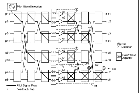
Referring to Figure 11 a feedback loop F1 is shown in more detail. Amplifiers
A1 and A2 are coupled between input hybrid 10 and output hybrid 12. Each
amplifier has a gain adjuster 14 and phase adjuster 16 located in its input
signal
path. A coupler 18 is provided at the signal node at the output of hybrid 12
where a null S1 is located. The coupler 18 has a coupling coefficient of at
least
25dB to ensure that insignificant power is taken from the amplifiers and to
minimise any hybrid imbalances caused through the inclusion of the coupler.
The coupler output is filtered by a preselect/image rejection filter 20,
downconverted by a mixer 22 to an intermediate frequency (IF), filtered by an
IF
filter 24 and then fed to an envelope detector 26. The detector output is
connected to the input of analogue to digital converter (ADC) 28, the output
of
which provides a digital signal representing the depth of the null S1. This is
fed
to a digital signal processor 30 which provides output control signals to the
gain
and phase adjusters 14 and 16 to minimise the null. Thus a feedback control
loop F1 is provided.
A local oscillator signal (LO) for the mixer 22 is derived from a frequency
generator unit (FGU) 32, which is also used to generate the pilot signal.
Generator 32 comprises a TCXO crystal oscillator 34 driving a frequency
multiplier 36 which multiplies up the TCXO frequency to the required pilot
signal
and the LO frequencies. The pilot signal is connected to the input port (p1)
of
the MPA by a coupler (not shown), also with a coupling coefficient of at least
25dB.
CA 02685191 2009-10-26
WO 2008/135753
PCT/GB2008/001553
- 14 -
The purpose of the preselect/image rejection filter is to prevent the null
detection circuitry from being overloaded by the total traffic through the
MPA,
and to reject signals at the IF image which may otherwise mask the null. The
mixer downconverts the null signal to a suitable IF where it can be filtered
by a
narrow band filter to isolate it from noise, thus ensuring that a null of the
required depth can be observed. Fluctuations in the detected null power caused
by noise can be suppressed either by a simple analogue filter after the
detector,
or by digital filtering within the DSP.
This arrangement for null detection assumes that the null depth can be
assessed just from measurements at the null port without reference to the
pilot
signal level. Such a scheme would be acceptable if it could be ensured that
after initial calibration of the null depth, variations in the system arising
from
thermal variations and ageing effects etc would not result in significant
changes
to the relationship between null power and required null depth. Such changes
could be guarded against by including a margin in the null depth equal to or
greater than the system variations. Otherwise a reference could be provided by
measuring the signal level at the other output port 40 of the hybrid 12 via an
additional coupler (not shown). This level would be compared directly by the
DSP with the null power to assess the null depth. Measurement of the reference
could be alternated with that of the null through an electronic switch. This
would
be located at the preselect/image filter input and would switch alternately
between the null and reference under the control of the DSP.
In order to reduce the equipment numbers associated with the feedback
scheme, the DSP and ADC and even more units such as the IF filtering and
amplification units could be single elements commutated with a suitable
periodicity between the seven feedback loops. This would be configured with
the input to the common elements (filter/ADC/DSP) switched sequentially
between the null points using electronic switches controlled by the DSP, and
with the DSP having 14 control outputs hard wired to the phase and gain
adjusters (7 of each).
As an alternative to the CW pilot signal, a carrier modulated by a direct
sequence spread spectrum (DSSS) waveform could be used for example with a
chip rate at 2MHz or more. This would operate with a suitable correlator
CA 02685191 2009-10-26
WO 2008/135753
PCT/GB2008/001553
- 15 -
replacing the narrow band IF filter to recover the carrier. This arrangement
may
be preferred if it is desired to reduce significantly the power spectral
density of
the pilot signal
An example of this scheme is presented here for operation at Ka-band
(20GHz). It is assumed that the pilot signal is CW and is located in that part
of
the satellite transmission spectrum free of traffic channels, for example that
part
of the downlink spectrum normally reserved for narrow band satellite beacon
and telemetry downlinks. A pilot signal frequency of 20.200GHz is assumed
with a corresponding local oscillator frequency of 20.150GHz. Thus an IF of
50MHz is selected ¨ low enough to allow the use of narrowband SAW or crystal
filter technologies. In order that the downconversion image is sufficiently
rejected, the preselect/image rejection filter must have a rejection of >40dB
at
20.100GHz. Such a filter can be implemented from a simple single dual mode
cavity design. After downconversion to the 50MHz IF, the null signal is
filtered
by a 10KHz wide crystal IF filter. This is wide enough to permit the use of a
relatively low cost, low stability TCXO (eg 1Oppm over life or 500Hz within
the IF bandwidth), but narrow enough to ensure that the transponder noise is
rejected to a level which does not significantly degrade the null depth.
For a worst case analysis, the noise falling in the null has been determined
for a
satellite communications payload operating with a minimum saturation flux
density SFD of -115dBW and MPA amplifier power of 130W (ie a total
transponder gain up to the amplifier output of 136.1dB). Assuming a typical Ka-
band transponder end-to-end system noise temperature of 600K (27.8dBK),
and Receive Section input demultiplexer DEMUX filtering in the vicinity of the
null of 25dB (which also provides protection of any neighbouring beacon and
telemetry downlinks), then the total noise falling within the null S1(in the
10KHz
IF bandwidth) is -49.7dBW. In the case of post DEMUX noise the total power
falling within the null is -48dBW (based on a total maximum post DEMUX
amplification of 106dB, with a typical noise figure of 10dB for the post DEMUX
section at maximum gain). In the case of intermodulation noise falling within
the
null, it is assumed that the system is transmitting 8 equal power carriers,
each
supporting a 45MSymbol/sec QPSK transmission, with amplifiers operating at
CA 02685191 2009-10-26
WO 2008/135753
PCT/GB2008/001553
- 16 -
2.5dB output back off. Assuming a typical carrier to 3rd order intermodulation
level C/Im of 15dB (for a linearised TWTA), and that the peak of the
intermodulation product falls on the null, then the product noise power in the
IF
bandwidth is -41.9dBW. The total from all three of the above noise sources is
then -40.4dBW.
In order that the null is not significantly affected by the noise, the minimum
null level should be at least 10dB above noise, ie at _>_-30.4dBW. Assuming a
minimum required null depth of 25dB (for an isolation of >30dB), then the
required pilot signal power at the output of each amplifier should be ?_0.35W,
say 0.5W. This represents a loss of only 0.03dB from the 130W amplifier
operating at 2.5dB output back off.
The formation of zeros or nulls of acceptable depth at the null points
presents
some difficulty as the depth is dependent on two variables ¨ amplitude and
phase (G & 0), and does not have a unique solution for non-zero cases. A
method in accordance with the invention to overcome this is to introduce a
phase deviation about the null, to identify or "seek out" a voltage minimum.
With
the phase then held to produce the identified minimum, the attenuation is then
adjusted to achieve the desired null depth. This process, as well as the
feedback, is carried out under the control of a digital signal processor
(DSP).
Referring to Figures 12 and 13, which are a diagram and flowchart of a
gain and phase adjustment process to achieve a desired null, this process
would be carried out at set intervals, with sufficient regularity to ensure
that the
MPA performance is held within specified limits. It starts with a measure of
the
current null depth D1 (see Figure 12), assumed in this case to be above, or to
the right of the null. If the null depth D1 is below the level Dreg, required
to
provide the desired isolation then no adjustments are made and the process is
stopped. Otherwise the phase adjuster is incremented in phase by one positive
step Oatep and the null re-measured. Again if the null depth is below the
level
Dreg, the process is stopped. If not, and if the second measurement is greater
than the first (Da in Figure 12), the phase increment Ostep is reversed in
sign and
then repeatedly added until either the null depth is below Dreq or until the
next
measurement is higher than its predecessor (eg measurement De compared
CA 02685191 2009-10-26
WO 2008/135753
PCT/GB2008/001553
- 17 -
with the previous measurement Db), at which point a single increment is
subtracted to bring the system back to the lowest null level (Db) that can be
achieved through phase adjustments alone. If the second measurement is
below the first (ie corresponding to the case in which the initial measurement
is
to the left of the null in Figure B), then no sign reversal is applied to the
phase
increment before the repeated addition. This process allows for the
possibility
of the null occurring midway between two increments, each of which produces
the same null level (D), and Dy in Figure 12). In this case the minimum
achievable null depth is taken as the last measurement (Dy).
If the required null depth cannot be obtained by phase adjustments alone,
then the process moves onto adjustment of gain G. This is done in exactly the
same manner as for the phase adjustments, but in this case the increments are
in steps of gain Gstep. During this process the phase is held at that value
which
resulted in the minimum null depth obtained from the phase adjustment
procedure described previously.
The whole of this process embodies a fail safe outcome, in that if no null can
be produced which is below the required level Dreq, then the process stops
when the minimum achievable null through both gain and phase adjustments
has been reached. Such a situation in which the required null level cannot be
attained may occur through failure of some component. However the resulting
isolation performance may still be acceptable.
The loops F1, F2 and F3 form a cascaded set with successive loops in the
cascade operating with nulls in the next hybrid column.
The first set of loops F1 operates from nulls in the first hybrid column, as
identified in Figs.3, 10, and operates on pairs of amplifiers (Ai/A2...A7/A8).
Referring to Eq.(6) & (7), a full set of nulls is obtained when the underlined
bracketed factors (Ai.Ci/J.Ciia + A2.C.2/J.C/2a), 643.C.HK.Cim + A4.C2/K.C120,
(45=C1ii...C//c+A6.C2IL.C/2c) & +
A8.C2im.C/2d) are all at zero. If a
null (S) is not obtained, then a control signal is fed back to a commandable
gain
and phase adjuster (G,0), prior to an amplifier (A1, A3, A5 & A7) within the
corresponding amplifier pair to achieve the null.
CA 02685191 2009-10-26
WO 2008/135753
PCT/GB2008/001553
- 18 -
As a consequence of nulls at the indicated 0/P ports of the first hybrid
column, the opposite hybrid ports will provide inphase summations of the
amplifier pair outputs (Ai/A2....A7/A8). These inphase summations are fed to
the
next (middle) column of hybrids. Referring to Eq.(8), nulls at the output of
these
hybrids is achieved when the highlighted factors [Ci/E.C//f44/.Ci/J.C21a +
A2.C21J.C22a) + C21E.C12f.(A3.C11K.C21b A4.C21K.C22b)1 &
1C11G.C1111.(A5.C111_.C21c
+ A6-C21L-C22c) + C21G.C1217.647-C11M.C21d A8.C21M.C22dE are zero. These two
expressions represent the inphase summation of amplifier pairs
(Ai/A2 ....................................................................
A7/A8) defined by the expressions in the innermost brackets, with
cancellation of these summations from adjacent pairs (Ai/A2 with A3/A4, and
A5/A6 with A7/A8), the same as shown in Fig.4. If nulls S2 are not obtained,
then
control signals are fed back in loops F2 to commandable gain/phase adjusters
prior to defined amplifiers (in this case A2, and AO.
The 0/P ports opposite to the null ports of the two hybrids in the middle
column provide inphase summations of sets of four amplifiers (Ai/A2/A3/A4 &
A5/A6/A7/A8). These inphase summations of four are fed to the last hybrid
column. Here the single null S3 (in this case at port 7) corresponds to the
cancellation of the two sets of four (A1/A2/A3/A4 with A5/A6/A7/A8) as defined
in
Eq.(9). Similarly if a null is not obtained here, then a control signal is fed
back in
feedback loop F3 to a gain/phase adjuster prior to a defined amplifier (in
this
case AO.
Note that there is one amplifier which does not have a gain/phase adjuster,
i.e. A4. There has to be one amplifier to act as the reference against which
all
the other units are ultimately matched. The selection of A4 is arbitrary and
any
other amplifier could equally well be chosen.
The sequencing or comparative reaction times of the loops are critical. The
fastest reacting loops are the innermost F1, which brings into alignment
(phase/amplitude match) the amplifiers pairs (A1/A2, .....................
A7/A8). After the pairs
have been aligned and allowed to settle, the next loops F2 acting through the
nulls in the middle hybrid column then come into play. These align groups of
four amplifiers (Ai/A2/A3/A4, A5/A6/k/A8). The final loop F3, acting through
the
null in the outermost hybrid column effectively aligns or matches all eight
amplifiers (after the middle loops have had time to settle), with the
resulting final
CA 02685191 2009-10-26
WO 2008/135753
PCT/GB2008/001553
- 19 -
summation occurring at the wanted output (in this case 0/P port 8). The whole
process of alignment will be recursive, since an adjustment produced by an
outer loop will influence an inner loop. For example, when the phase/amplitude
adjuster associated with A2 to achieve the null in the middle column is
altered,
the adjuster associated with A1 may need to change to maintain the null in the
first column. This whole recursive process, which will have the global
objective
of achieving nulls at all the identified points, will be an extended
procedure.
However, the varying factors which would cause the loops to apply adjustments
would be slowly time variant. These would include component ageing, thermal
variations caused for example by diurnal changes in the spacecraft
temperatures, and traffic variations which may also be of a diurnal nature.
Thus
once the feedback system has acquired the nulls and has settled, maintenance
of tracking should be fairly uneventful.
The process described above, acting with the null points identified and with
the pilot signal injected as indicated will provide active matching for the
matrix
elements highlighted in Figure 7. The corresponding output port isolations and
level at the wanted ports (related to combining loss) will be under the direct
control of the feedback scheme. The remaining elements will be under indirect
control, in that the nulls for these cases will be related to the controlled
nulls, but
will have a residual voltage dependent on the quality (phase and amplitude
matching) of the individual hybrids or INET and ONET as a whole. Since this
relationship is essentially exclusively defined by the INET and ONET matching,
the basic difficulty of ensuring acceptable tracking of the amplifiers will
have
been avoided. Isolation performance will now depend essentially on the
stability
of passive units such as machined waveguide parts which should be high.
However, this will be true in the vicinity of the pilot signal frequency. Away
from
this frequency there may be contributions to the residual null voltage arising
from frequency related tracking errors between the amplifiers and hybrids over
a wide band.
Techniques which may be employed to reduce the effect of these errors
include use of multiple pilot signals distributed across the band, switched
frequency or frequency hopped signals and wideband, DSSS (Direct Sequence
Spread Spectrum) modulated carriers. Various combinations of these
CA 02685191 2009-10-26
WO 2008/135753
PCT/GB2008/001553
- 20 -
techniques may also be used, for example multiple signals distributed across
the band, each of which is DSSS modulated. The application of these
techniques would produce null measurements relating to the mean performance
of the MPA across the band rather than at a single spot frequency.
Correspondingly, the isolation and combining performance of the equipment
would be better aligned for wideband operation.
Simulation Results
In order to assess the effectiveness of the feedback loops, a model was
developed representing the MPA system illustrated in Fig.10. Individual models
were derived for the INET, combined amplifier and gain/phase adjusters and
ONET, which were then cascaded to provide a model for the overall MPA.
As previously stated, the achieved port isolation is a function of the
amplitude
and phase deviations of the individual components around their nominal values.
If these components were ideal then infinite isolation would be obtained
between the wanted outputs and the unwanted outputs, but as they are not
ideal a finite isolation results. The amplitude and phase deviations for each
component have been modeled as Gaussian random variables with the mean
values and variances presented in the Table above.
These values are
considered as being practicable at Ku/Ka band.
The values quoted for the hybrids have been used for both the INET and
ONET, and correspond to those expected for waveguide hybrids. The amplifier
values are based on expected performance for a 130W Ka-band TWTA.
The distributions obtained for each of the components are presented in
Fig.14 to Fig.17.
As described above, three feedback loops F1 ¨F3 are employed to maintain
the output port isolation below a desired threshold. With reference to Fig.1
and
Component Mean GO Variance (3o) Fig.10:
Hybrid:
Loss (dB) -3.25 0.23 a.
The innermost loops
Phase Deviation ( ) 0.0 3.0
F1 provide feedback
Amplifier:
Relative Gain (dB) 0.0 2.0
from output hybrids
Relative 0.0 10.0
Phase ( )
Component Parameters
CA 02685191 2009-10-26
WO 2008/135753
PCT/GB2008/001553
-21 -
Ha, Hb, Hc and Hd (first column) to the gain/phase adjusters
associated with amplifiers A1, A3, A5 and A7 respectively.
Expressions for the null ports can be derived from Eq.(6) and are
given by:
Cii a.CiiJ.Pki .131 =eXPjApi C12a. C21J.A2432.expj. (P2 =O (14)
Clib=Ci1K.A3.133.expjAp3 + Cl 2b=C21K.A4 = 0
(15)
CIIC.CIIL.A5.135.expj.(p5 Cl 2c.C21L=A6.136.expjAp6 = 0
(16)
Clid=Ciim.A7.137.expjAp7 + C12d=C2im.A8.138.expjAp8 = 0
(17)
b. The middle loops F2 provide feedback from the output hybrids Hf
and Hb (second column) to the gain / phase adjusters associated
with amplifiers A2 and A6. Expressions for the null port can be
derived from Eq.(8) and are given by:
Clif.CliE=( C2ia=Citi.Ai.pi.expj=Ti + C22a=C21J.A2.132.expj(p2)+
C12f.C21E=(Clib=CiiK.A3.133.expj(p3 + C22b=C21K.A4.) = 0
(18)
Cii h.C11G=(C21c= C11L.A5.135.expl. (P5 + C22c.C211...A6=136.expj(p6) +
C12h=C2iG=(C21d=Ciim.A7.137.expj(p7 + C22d=C2im.A8.138.expjAp8) = 0
(19)
c. The outermost loop F3 provides feedback between output hybrid
Hm (third column) to the gain / phase adjuster associated with
amplifier A8. The null port expression can be derived from Eq.(9)
and is given by:
Ciim=CliA.[C2if.CliE=(C2ia=CiiJ.A1.131.expjApi + C22a=C21J.A2.132.expjA(p2)
+Ci2f.C21E=(C2ib=CiiK.A3433.expj(p3 + C22b=C2iK=A4)] +
C12m = C21A= [C21h = C11G = (C21c= C111..A5=P5.expj=T5 C22c.C21L.A6.136.expj
(p6)
4-C22h=C2iG=(C2id=Ciim.k.137.expjAp7 + C22d=C2im.A8.P8.expj(p8)] = 0 (20)
where the terms pi.expjApi represents the magnitude and phase
coefficients of the gain / phase adjuster. As amplifier A4 provides
acts as the reference there is no gain / phase adjustment
associated with it.
From Eqs (14) thru (20) it can be seen that the null port expressions are
dependent upon each other; changes made to the gain / phase adjusters in one
CA 02685191 2009-10-26
WO 2008/135753
PCT/GB2008/001553
- 22 -
feedback loop will affect the performance of the other feedback loops.
Therefore, finding the minimum target isolation across the MPA becomes an
iterative process.
The adopted methodology was to initially set each gain / phase adjuster
to provide unity gain and zero phase shift. The null port expressions for the
inner loop are then solved for131, 133, 1351 137, 91, 93, 98, and 97. Once
these gain /
phase adjustments are applied, the null port expressions for the middle loop
are
then solved for 132, 138, 92, and 96. This process is then repeated until
convergence occurs: the point where a change in the middle loop's coefficients
does not cause a change in the inner loop's coefficients. When this position
is
reached, the outer loop null port expression is then solved (provided the
current
isolation was less than the minimum target isolation) for 138 and 98, causing
the
inner and middle loops to re-converge. This procedure is repeated until the
minimum target isolation of the MPA is met, and is considered to be
representative of how the system would operate in practice with the inner loop
having the fastest time constant and the outer loop having the slowest.
Results of simulations are provided in Fig.18 and Fig.19, below using the
inner and middle feedback loops.
Figure 18, provides the isolation matrix for the MPA prior to any feedback
being applied, where each row of the matrix represents an output port (top row
= one) and each column represents an input port (left hand column = 1).
Therefore, the isolation between input port 1 and output port is given by lii
and
is 20.8dB. The minimum isolation target for the feedback loops was 25dB ¨ the
degree of isolation that may be applicable to an SFB payload.
As can be seen from Fig.19, there has been a significant improvement in
the isolation performance of the MPA. It should be noted that only the inner
and
middle feedback loops were used. The isolation in the quadrant denoted 'X'
(Figure 7), has been improved, by up to 20dB, due to the inner feedback loop.
However, because of factors such as noise effects and limited resolution in
the
phase/amplitude compensations, isolations in excess of 30dB would most likely
not be achieved in practice. Within the quadrant denoted '11' (Figure 7),
smaller
but notable isolation improvements have been achieved; typically around 6dB to
CA 02685191 2009-10-26
WO 2008/135753
PCT/GB2008/001553
- 23 -
8dB. In the quadrants denoted by 'Z' (e.g. 4081), the isolation has
deteriorated.
This has happened for two reasons. The first is that the outermost feedback
loop was not included in the simulation, and the second is that without the
outermost feedback loop, the adjustments made to the gain / phase shifters by
the inner and middle feedback loops would have an effect on the isolation at
these points. The actual effect would be determined by the variances of the
transmission coefficients in the associated paths, and equally could have
improved rather than deteriorated. It is fully expected that the inclusion of
the
outermost feedback loop would have also provided improved isolation
performance in quadrant 2'.