Note: Descriptions are shown in the official language in which they were submitted.
CA 02685477 2014-10-24
=
- 1 -
HIGH-EFFICIENT LIGHT ENGINES USING LIGHT EMITTING DIODES
BACKGROUND OF THE INVENTION
Solid state light emitting devices, including solid state lamps having light
emitting diodes (LEDs), laser diodes (LDs), and resonant cavity LEDs (RCLEDs)
are
extremely useful, because they potentially offer lower fabrication costs and
long term
durability benefits over conventional incandescent and fluorescent lamps. Due
to their
long operation (burn) time and low power consumption, solid state light
emitting
devices frequently provide a functional cost benefit, even when their initial
cost is
greater than that of conventional lamps. Because large scale semiconductor
manufacturing techniques may be used, many solid state lamps may be produced
at
extremely low cost.
In addition to applications such as indicator lights on home and consumer
appliances, audio visual equipment, telecommunication devices and automotive
instrument markings, LEDs have found considerable application in indoor and
outdoor
informational displays.
With the development of efficient LEDs that emit short wavelength (e.g.,
blue or ultraviolet (UV) radiation), it has become feasible"to produce LEDs
that
generate white light through down conversion of a portion of the primary
emission of
the LED to longer wavelengths. Conversion of primary emissions of the LED to
longer
wavelengths is commonly referred to as down-conversion of the primary
emission. An
unconverted portion of the primary emission combines with the light of longer
wavelengths to produce white light.
Phosphor conversion of a portion of the primary emission of the LED chip
is attained by placing a phosphor layer in an epoxy that is used to fill the
reflector cup
which houses the LED chip within the LED lamp. The phosphor is in the form of
a
powder that is mixed into the epoxy prior to curing the epoxy. The uncured
epoxy
slurry containing the phosphor powder is then deposited onto the LED chip and
subsequently cured.
The phosphor particles within the cured epoxy generally are randomly
oriented and interspersed throughout the epoxy. A portion of the primary
radiation
emitted by the LED chip passes through the epoxy without impinging on the
phosphor
particles, and another portion of the primary radiation emitted by the LED
chip
impinges on the phosphor particles, causing the phosphor particles to emit
longer
CA 02685477 2009-10-27
WO 2008/027093 PCT/US2007/012311
- 2 -
wavelength radiation. The combination of the primary short wavelength
radiation and
the phosphor-emitted radiation produces white light.
Current state of the art phosphor-converted white LED (pc-LED)
technology is inefficient in the visible spectrum. The light output for a
single pc-white
LED is below that of typical household incandescent lamps, which are
approximately 10
percent efficient in the visible spectrum. An LED device having a comparable
light
output than that of a typical incandescent lamp necessitates a larger LED chip
or a
design having multiple LED chips. Moreover, a form of direct energy absorbing
cooling
must be incorporated to handle the temperature rise in the LED device itself.
More
particularly, the LED device becomes less efficient when heated to a
temperature
greater than 100 C., resulting in a declining return in the visible spectrum.
The
intrinsic phosphor conversion efficiency, for some phosphors, drops
dramatically as the
temperature increases above approximately 90 C threshold. Other down
conversion
materials like quantum dots could start to decrease in efficiency from even
lower
temperatures, 25 degrees centigrade.
SUMMARY OF THE INVENTION
An exemplary embodiment of the invention is a light emitting apparatus
having a light source for emitting short wavelength radiation and an optic
device
configured to receive the short wavelength radiation emitted from the light
source. A
device directs at least some of the short wavelength radiation emitted from
the light
source into the optic device and a down conversion material receives at least
some of
the short wavelength radiation directed into the optic device in one spectral
region and
emits radiation in at least one other spectral region.
Another embodiment of the invention is a light emitting apparatus having
a light source for emitting multi-colored radiation and an optic device
configured to
receive at least a portion of the multi-colored radiation. A device directs at
least some
of the multi-colored radiation emitted by the radiation source into the optic
device. A
diffuser material coupled to the optic device receives at least some of the
multi-colored=
radiation and converts the received multi-colored radiation into forward
transferred
radiation and back transferred radiation. The optic device is configured to
extract at
least a portion of the back transferred radiation from the optic device.
BRIEF DESCRIPTION OF THE DRAWINGS
The invention is best understood from the following detailed description
when read in connection with the accompanying drawing. It is emphasized that,
according to common practice, the various features of the drawing are not to
scale. On
the contrary, the dimensions of the various features are arbitrarily expanded
or reduced
for clarity. Included in the drawing are the following figures:
CA 02685477 2009-10-27
WO 2008/027093 PCT/US2007/012311
- 3 -
Fig. 1 is a simplified illustration of an optic device;
Fig. 2 is another simplified illustration of an optic device with a device to
collect light that may be extracted from the optic device;
Fig. 3 is partial cross-sectional view of an exemplary embodiment of the
present invention;
Figs. 4A-4E illustrate alternative shapes of an optic device that may be
used with an exemplary embodiment of the present invention;
Fig. 5 illustrates an exemplary embodiment of apertures that may be
disposed in an exemplary embodiment of the present invention;
Fig. 6 illustrates exemplary effects of an exemplary light ray inside an
optic device in accordance with an exemplary embodiment of the present
invention;
Fig. 7 is an exploded view of an alternative embodiment of the present
invention;
Fig. 8 is a partial cross-section view of another alternative embodiment of
the present invention;
Fig. 9 is a exploded view of yet another alternative embodiment of the
present invention;
Fig. 10 is a partial cross-section view of another embodiment of the
present invention;
Fig. 11 is an exploded view of an another alternative embodiment of the
present invention;
Fig. 12 is a diagram illustrating the exemplary radiation rays that result
when an exemplary radiation ray from a short-wavelength LED chip impinges on a
layer
of down conversion material;
Fig. 13A is a partial cross-section view and a partial perspective view of
another embodiment of the present invention;
Fig. 13B is a bottom view of an end of the embodiment shown in Fig.
13A;
Fig. 13C illustrates a ray tracing simulation of the embodiment shown in
Fig. 13A;
Fig. 13D illustrates a ray tracing simulation for an embodiment that is
different from the embodiment shown in Fig. 13A; and
Fig. 14 is a graph showing how much light may be extracted from the
bottom of an optic device under varying conditions.
DETAILED DESCRIPTION OF THE INVENTION
Fig. 12 is a diagram illustrating the exemplary radiation rays that may
result when an exemplary radiation ray 2000 from a short-wavelength LED chip
2002
CA 02685477 2009-10-27
WO 2008/027093 PCT/US2007/012311
- 4 -
impinges on a layer of down conversion material 2004. The impingement of
exemplary
short-wavelength radiation 2000 from a short-wavelength source such as an LED
chip
2002 onto a down conversion material layer 2004 may produce radiation with
four
components: back transferred short-wavelength radiation 2006 reflected from
the down
conversion material layer 2004; forward transferred short-wavelength radiation
2008
transmitted through the down conversion material layer 2004; forward
transferred
down-converted radiation 2010 transmitted through the down conversion material
2004; and back transferred down-converted radiation 2012 reflected from the
down
conversion material 2004. The four components may combine to produce white
light.
Two of the four components 2010 and 2012 may each be comprised of
two sub-components. One of the sub-components of forward transferred down-
converted radiation may be emitted radiation 2014; i.e., down-converted
radiation
having a longer wavelength than the short-wavelength radiation that impinges
onto the
down conversion material layer 2004. The emitted radiation sub-component 2014
of
forward transferred down-converted radiation may be produced by short-
wavelength
radiation 2000 impinging on particles of the down conversion material 2004 as
it is
transmitted through the down conversion material 2004. The second sub-
component of
forward transferred down-converted radiation may be forward scattered emitted
radiation 2016; i.e., other down-converted radiation having a longer
wavelength than
the short-wavelength radiation 2000 that impinges onto the down conversion
material
layer 2004. The forward scattered emitted radiation sub-component 2016 of
forward
transferred down-converted radiation 2010 may be produced by short-wavelength
radiation 2000 impinging on particles of the down conversion material 2004 and
that
also bounces back and forth on the particles of the down conversion material
2004
before being transmitted through the down conversion material 2004.
One of the sub-components of back transferred down-converted radiation
2012 may be emitted radiation 2020; i.e., down-converted radiation having a
longer
wavelength than the short-wavelength radiation 2000 that impinges onto the
down
conversion material layer 2004. The emitted radiation sub-component 2018 of
back
transferred down-converted radiation 2012 may be produced by short-wavelength
radiation 2000 impinging on particles of the down conversion material 2004 as
it is
reflected from the down conversion material 2004. The second sub-component of
back
transferred down-converted radiation 2012 may be back scattered emitted
radiation
2020; i.e., other down-converted radiation having a longer wavelength than the
short-
wavelength radiation 2000 that impinges onto the down conversion material
layer
2004. The back scattered emitted radiation sub-component 2020 of back
transferred
down-converted radiation 2012 may be produced by short-wavelength radiation
2000
CA 02685477 2009-10-27
WO 2008/027093 PCT/US2007/012311
- 5 -
impinging on particles of the down conversion material 2004 and that also
bounces
back and forth on the particles of down conversion material 2004 before being
reflected
from the down conversion material 2004.
White light may be produced by the combinations of the various
=
components discussed above. In the forward transferred direction (i.e., for
radiation
2008, 2014, 2016, 2010 that is transmitted through the down conversion
material
layer), white light may be produced by the combination of forward transferred
short-
wavelength radiation 2008 with either or both of the sub-components 2014, 2016
of
the forward transferred down-converted radiation 2010. That is, white light
may be
produced in the forward transferred direction by the combination of forward
transferred
short-wavelength light 2008 with transmitted emitted radiation 2014 and/or
with
transmitted forward scattered emitted radiation 2016.
In the back transferred direction (i.e., for radiation 2006, 2018, 2020,
2012 that is reflected from the down conversion material layer), white light
may be
produced by the combination of back transferred short-wavelength radiation
2006 with
either or both of the sub-components 2018, 2020 of the back transferred down-
converted radiation 2012. That is, white light may be produced in the back
transferred
direction by the combination of back transferred short-wavelength light 2006
with
reflected emitted radiation 2018 and/or with reflected back scattered emitted
radiation
2020.
The wavelength of the forward transferred short-wavelength radiation
2008 may be about the same as the wavelength of the radiation 2000 emitted by
a
radiation source such as an LED chip 2002. The wavelength of the back
transferred
short wavelength radiation 2006 may be about the same as the wavelength of the
radiation 2000 emitted by the radiation source 2002. The wavelength of the
forward
transferred short-wavelength radiation 2008 may be about the same as the
wavelength
of the back transferred short-wavelength radiation 2006. In an exemplary
embodiment, the radiation source 2002 may emit radiation exhibiting a
wavelength
that is less than 550 nm, more particularly in a range of about 200 nm to less
than 550
nm. Accordingly, the wavelength of the forward transferred short-wavelength
radiation
2008 and the wavelength of the back transferred short-wavelength radiation
2006 may
be less than 550 nm, more particularly in a range of about 200 nm to less than
550
nm.
The wavelength of the forward transferred down-converted radiation
2010 (including its sub-components 2014, 2016) and the wavelength of the back
transferred down-converted radiation 2012 (including its sub-components 2018,
2020)
may be any wavelength that is longer that the excitation spectrum of the down
CA 02685477 2009-10-27
WO 2008/027093 PCT/US2007/012311
- 6 -
conversion material 2004. In an exemplary embodiment, the excitation spectrum
of
the down conversion material 2004 may be in the range of about 300 nm to about
550
nm. In alternative embodiments, other down conversion materials may be used
that
have an excitation spectrum other than in the range of about 300 nm to about
550 nm.
The excitation spectrum of the down conversion material 2004 should produce
radiation
having a wavelength that is longer than the wavelength of the radiation
produced by
the short-wavelength emitting radiation source 2002. In an exemplary
embodiment,
the down conversion material 2004 may produce radiation in the range of from
about
490 nm to about 750 nm.
To increase the light output from a phosphor-converted white LED (pc-
LED) and to achieve higher luminous efficacy, the down-conversion material
(e.g.,
phosphor or quantum dots) is removed to a remote location and a properly
tailored
optic device is placed between the LED chip and the down-conversion material
layer.
Then, the back transferred light can be extracted to increase the overall
light output
and efficacy. This technique significantly increases the overall light output
and
luminous efficacy of a pc-white LED by extracting the phosphor emitted and
back
scattered reflected radiation, and the reflected short-wavelength radiation
that
otherwise would be lost. The invention described in this specification may
achieve a
1500-lumen package at 150 lm/W, for example, using an LED chip array. In an
exemplary embodiment, the LED chip array may be nitride-based. In alternative
embodiment, the LED chip array may be AlInN-based or any other short
wavelength
emitter.
Figs. 1 and 2 are simplified illustrations of an optic device to enable a
discussion of the general concepts of capturing and extracting back
transferred
radiation from a down conversion material as may be used in various
embodiments of
the invention. Fig. 1 illustrates an optic device making use of a down
conversion
material that is remote from a short wavelength radiation emitter. The down
conversion material may be a phosphor. As shown, device 600 includes short
wavelength radiation emitter 602 separated from down conversion material
(here, a
phosphor (or quantum dot) layer) 604 by optic device 606 which may be a
transparent
medium, such as air, glass, or acrylic, for example. Phosphor (or quantum dot)
layer
604 may be mounted or deposited on optic device 606 having walls 610 and 612
that
are substantially transparent and light transmissive. Phosphor (or quantum
dot) layer
604 may include additional scattering particles (such as micro spheres) to
improve
mixing of light of different wavelengths. Also the phosphor (or quantum dot)
layer 604
may be a single phosphor (or quantum dot) or multiple phosphors (or quantum
dots)
to produce different colored down-converted radiation that may be in several
different
CA 02685477 2009-10-27
WO 2008/027093 PCT/US2007/012311
- 7 -
spectral regions. Alternatively, a layer with scattering particles only may be
placed
above, below, or above and below the down conversion material layer to improve
color
mixing.
Short wavelength radiation emitter 602 may be located between walls
610 and 612. Both the short wavelength radiation emitter 602 and the optic
device
606 are positioned on a base 603. Radiation rays 614 may comprise radiation
transmitted through the phosphor layer 604 including forward transferred short-
wavelength radiation transmitted through the phosphor layer 604 and forward
transferred down-converted radiation transmitted through the phosphor layer
604.
Radiation rays 615 may comprise back transferred short-wavelength radiation
and back
transferred down-converted reflected radiation that may be emitted and/or
scattered
back by phosphor layer 604. Radiation rays 616 may comprise the radiation rays
615
that are transmitted through the substantially transparent light transmissive
walls 610
and 612. Accordingly, both radiation rays 615 and radiation rays 616 may
include
short-wavelength radiation reflected from the phosphor layer 604 and down-
converted
reflected radiation that may be emitted and/or scattered from the phosphor
layer 604.
In an exemplary embodiment, some or all of radiation rays 615 and/or 616 may
be
seen as visible light.
Use of optic device 606 allows the short-wavelength radiation and down-
converted radiation that otherwise would be reflected back into the short
wavelength
radiation emitter 602 to be advantageously transmitted (alternatively referred
to as
extracted) to the exterior or outside of the optic device 606, through the
transmissive
properties of the optic device 606.
Fig. 2 illustrates another optic device. As shown, device 700 includes
optic device 600 disposed within reflector 702. In Fig. 2, reflector 702 has a
geometric
shape of a parabola for illustration purposes, but it may take any geometric
shape.
Substrate 603 may be used for mounting short wavelength radiation emitting
source
602, one end of optic device 606, and one end of reflector 702. Light rays 616
that
may be transmitted through walls 610 and 612 of optic device 606 may impinge
on..
reflector 702 which redirects them forward as light rays 714. Advantageously,
the
direction of light rays 714 are desirably generally in the same direction as
light rays
that have been transmitted through the phosphor layer. Consequently, the total
light
output of the device 600 may be a combination of light transmitted through the
phosphor layer and light rays 714.
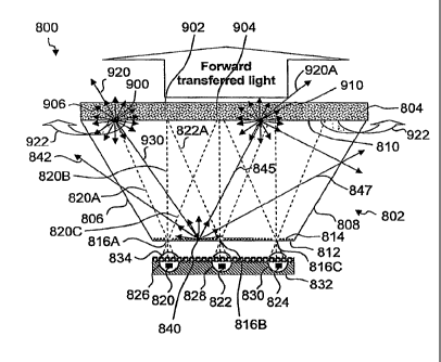
Fig. 3 illustrates an exemplary embodiment of the present invention. In
Fig. 3, device 800 includes optic device 802 which may be a transparent medium
such
as air, glass, acrylic, or any other medium allowing the transmission of
light. Optic
CA 02685477 2009-10-27
=
=
WO 2008/027093
PCT/US2007/012311
- 8 -
device 802 may have substantially transparent light transmissive walls 806 and
808.
Optic device 802 may be configured and designed to extract light from inside
the optic
device 802 to outside the optic device 802. Although optic device 802 is
illustrated in
Fig. 3 as a four-sided device, it will be understood that optic device may
have fewer or
more than four sides. It will also be understood that optic device may be in
the shape
of a cylinder or may have some other round shape.
A down conversion material layer 804 may be mounted, coated, or
deposited on portion 810 of optic device 802. In an exemplary embodiment,
portion
810 may be an end of optic device 802. In an alternative embodiment, portion
810
may be located at a position other than at an end of optic device 802. A down
conversion material is a material that absorbs radiation in one spectral
region and
emits radiation in another spectral region. In an exemplary embodiment, down
conversion material layer 804 may comprise a single down conversion material.
In an
alternative embodiment, the down conversion material layer 804 may comprise
more
than one down conversion material. In exemplary or alternative embodiments,
the
down conversion material layer may comprise one or more phosphors such as
YAG:Ce,
YAG:ce phosphor plus Eu phosphor; YAG:Ce phosphor plus cadmium-selenide (CdSe)
or
other types of quantum dots created from other materials including lead (Pb)
and
silicon (Si); and other phosphors that have been identified in a copending PCT
application filed on June 20, 2006 (Attorney Docket RPI-143W0). In an
alternative
embodiment, the phosphor layer may comprise other phosphors, quantum dots,
quantum dot crystals, quantum dot nano crystals, or other down conversion
material.
The down conversion region may be a down conversion crystal instead of
powdered
material mixed into a binding medium. All of the embodiments disclosed in this
application may use any of the phosphors described herein.
In an exemplary embodiment, end 810 of optic device 802 may be
substantially flat. Figs. 4A-4E depict alternative geometric shapes of optic
device 802.
Alternative optic device 8010 illustrated in Fig. 4A is of a conical geometry
having a top
surface 8012. Alternative optic device 8020 illustrated in Fig. 4B is of a
spherical
geometry having a top surface 8022. Alternative optic device 8030 illustrated
in Fig.
4C is of a hyperbolic geometry having a top surface 8032. Alternative optic
device
8040 illustrated in Fig. 4D is of a pyramidal geometry having a top surface
8042.
Alternative optic device 8050 illustrated in Fig. 4E is of a box-shaped
geometry having
a top surface 8052. In an exemplary embodiment, and in the alternative
embodiments
illustrated in Figs. 4A-4E, top surfaces 810, 8012, 8022, 8032, 8042, and 8052
may be
substantially flat, or may have another shape, such as arcuate, for example.
The down
conversion material may not cover the entire top surface. Instead it may cover
only
CA 02685477 2009-10-27
WO 2008/027093 PCT/US2007/012311
- 9 -
part of the top surface and may cover it in a pattern. The down conversion
material
may include additional non down converting scattering particles such as
microspheres.
Alternatively, a layer of scattering particles such as non down converting
particles may
be placed only above, only below, or both above and below the down conversion
material layer to improve color mixing.
Returning to Fig. 3, the transfer (extraction) of radiation through walls 806
and
808 may occur because optic device 802 may be configured and designed with
substantially transparent, substantially light transmissive walls 806 and 808
to extract
radiation from inside optic device 802 to outside optic device 802. In
addition, various
dimensions of optic device 802 may be varied in order to extract a desired
amount of
radiation out of the optic device 802. The dimensions that may be varied are
the width
at the end 810 and the width at the end 812. Similarly, widths between walls
806 and
808 at one or more points between ends 810 and 812 may be varied. Varying the
widths between ends 810 and 812 may result in ,walls 806 and 808 being
substantially
straight, curved, or having both straight and curved portions.
The dimensions and shapes of the features of the optic device 802
discussed above may be varied depending upon .the application to which the
optic
device 802 may be used. The dimensions of the features of optic device 802 may
be
varied, and set, by using the principles of ray tracing and the principles of
total internal
reflection (TIR). When principles of TIR are applied, reflectivity of
radiation off of one
or both walls 806 and 808 may exceed 99.9%. The principles of TIR may be
applied to
all of the embodiments disclosed in this application and their application is
discussed
again below.
= As shown in Fig..3, an exemplary embodiment of the device 800 may
have three short-wavelength radiation emitters (called light sources
hereafter) 820,
822, 824 positioned adjacent portion 812 of optic device 802. In an exemplary
embodiment, portion 812 may be located at an end of optic device 802 and may
be
opposite end 810. In an alternative embodiment, portion 812 may be located at
a
position other than at an end of optic device 802. Light sources 820, 822, 824
may
each be a semiconductor light emitting diode such as a light emitting diode
(LED), a
laser diode (LD), or a resonant cavity light emitting diode (RCLED). In an
exemplary
embodiment, some or all of the light sources may transmit short- wavelength
radiation
toward down conversion material 804 in order to create white light. Although
Fig. 3
shows three light sources, it will be understood that fewer or more light
sources may be
used.
As shown in Fig. 3, light sources 820, 822, and 824 may all positioned
outside of end 812 of optic device 802. Light sources 820, 822, and 824 may be
CA 02685477 2009-10-27
WO 2008/027093 PCT/US2007/012311
- 10 - -
positioned inside respective reflectors 826, 828, and 830 which may also be
positioned
outside of end 812. The reflectors 826, 828, and 830 may direct at least some
of the
short wavelength radiation emitted from the light sources 820, 822, and 824
into the
optic device 802. In an exemplary embodiment, reflectors 826, 828, and 830 may
exhibit a concave geometric shape. In alternative embodiments, reflectors 826,
828,
and 830 may exhibit a parabolic shape, an elliptical shape, or a flat shape.
If an
embodiment of the reflectors exhibits a flat geometric shape, an epoxy may be
placed
around each of the light sources to hold them in place. The reflectors 826,
828, and
830, with the respective light sources 820, 822, and 824, may be mounted into
a base
832. A micro lens 834 may be disposed above reflectors 826, 828 and 830 and
between the light sources and end 812. In exemplary embodiment, micro lens 834
may be placed across the top of base 832. Micro lens 834 may be in the form of
a
sheet of individual elements. Micro lens 834 may be a portion of the device
that directs
at least some of the light from light sources 820, 822, 824 into optic device
802. Micro
lens 834 may be disposed between the light sources and the optic device. The
purpose
of micro lens 834 may be to focus radiation from light sources 820, 822, 824
through
apertures 816A, 816B, and 816C, discussed in more detail below. If the
reflectors 826,
828, 830 focus a sufficient amount of radiation into respective apertures,
then micro
lens 834 may not be needed.
Although Fig. 3 illustrates three light sources and three reflectors, an
alternative embodiment of the invention may have nine light sources and nine
reflectors, for example. The light sources may all be the same size or they
may be
different sizes, depending on the quantity of light output that is desired.
The light
sources may be arranged in a variety of configurations, such a circular, oval,
or linear.
Other numbers of light sources and reflectors may be used. For example, an
array of 3
x 24 light sources and reflectors may be used.
If the light sources are laser diodes (LD), the light beam may be
collimated and, instead of a micro lens 834, a graded index (GRIN) lens, ball
lens, or
any other lens may be placed between the light sources and the optic device to
direct
the short wavelength radiation transmitted by the laser diodes in a desired
direction. If
the light sources are LEDs, a parabolic or elliptical reflector may be used
along with a
lens to direct the light. Alternatively, LEDs may be used with a reflector
alone, without
a lens, in which case the reflector may direct the light in a desired
direction. In any of
these embodiments, a lens may be used to better direct the radiation, thereby
increasing coupling capacity. However, if cost is a consideration, the lens
may be
eliminated. Any of the referenced micro lens, GRIN lens, ball lens, or other
lens, and
reflectors may be referred to as a device for directing short wavelength
radiation
CA 02685477 2009-10-27
WO 2008/027093 PCT/US2007/012311
=
- 1 1 -
emitted from a radiation source into the optic device. The source for emitting
short
wavelength radiation may also be referred to as a short wavelength radiation
emitter.
As shown in Figs. 3, 5 and 6, end 812 of optic device 802 may have an
inside surface 814. In an exemplary embodiment, inside surface 814 of end 812
may
be a reflective white surface having a reflectivity of about 70% or higher. In
an
alternative embodiment, the reflective surface may be other than white and may
have
a reflectivity other than 70%. In an exemplary embodiment, inside surface 814
may be
part of the optic device 802. In an alternative embodiment, a reflective plate
may be
placed on top of the inside surface of end 812. If a reflective plate is used,
it may be
made of any material that provides a reflective surface or that would support
a
reflective surface. Regardless of how the reflective surface is formed or
applied, the
reflective surface may have a smooth surface, it may have bumps on its
surface,
conical sections on its surface, or any other finish on the surface that may
enhance the
reflectivity of the inside surface.
End 812 may have a plurality of very small apertures in it. Figs. 3 and 6
illustrate three apertures, 816A, 816B, and 816C. The apertures 816A, 816B,
and
816C may be configured to allow at least some of the radiation from the light
sources
820, 822, 824 to be transferred into the optic device. In an exemplary
embodiment, a
diameter of the apertures may be selected from a range of about 0.2 mm to
about 1
mm. In alternative embodiments, the diameters of the apertures 816A, 816B, and
816C may be selected from a range of about 1 mm to about 3 mm. The diameters
of
the apertures may be selected to be sufficiently small in order to minimize
the amount
of back transferred radiation from phosphor layer 804 that may escape through
the
apertures 816A, 816B, and 816C. Also if a reflective plate is used, there may
be a
number of apertures or, alternatively, transparent areas in the reflective
plate. The
number of apertures or transparent areas may desirably equal the number of
light
sources. Fig. 5 illustrates the apertures as black dots, solely for
illustrative purposes in
order to distinguish the apertures from the white paper. Fig. 5 also
illustrates an
exemplary embodiment having an array of nine apertures. It will be understood
that
more or fewer apertures may be used than what is illustrated in Figs. 3, 5,
and 6. As*
mentioned above, the number of apertures may desirably equal the number of
light
sources.
Respective apertures may be aligned with respective light sources so that
at least some of the radiation emitted from each light source may be
transferred
through a respective aperture into the optic device. In an alternative
embodiment,
very small transparent areas may be provided in end 812 and in the inside
reflective
surface 814 instead of apertures. The diameter of the alternative embodiment
CA 02685477 2009-10-27
WO 2008/027093 PCT/US2007/012311
- 12 -
transparent areas may be the same as the diameter of the apertures in the
exemplary
embodiment. Again, the number of transparent areas may desirably equal the
number
of light sources. Inside surface 814 may be highly reflective over its entire
surface
except at the locations where light from the light sources may enter optic
device 802
through the apertures or transparent areas.
The apertures (or alternative transparent areas), such as apertures 816A,
816B, and 816C, may be aligned with the light sources 820, 822, and 824 so
that
respective devices for directing the radiation may direct the radiation from
the light
sources into optic device 802 through the respective apertures or,
alternatively,
through the respective transparent areas. For illustration purposes, we will
describe
the operation and effect of radiation emitted from light source 820. It will
be
understood that the operation and effect of radiation emitted from light
sources 822
and 824, and from any additional light sources m' ay be the same as the
operation and
effect of radiation emitted from light source 820.
Referring, for illustration purposes, to light source 820, exemplary
radiation rays 820A, 820B, and 820C may be transmitted from light source 820
through
aperture 816A and may impinge on phosphor layer 804 at exemplary impingement
points 900, 902, and 904. It will be understood by those skilled in the art,
that more or
fewer radiation rays may be transmitted by light source 820 and may impinge on
phosphor layer 804 in more or fewer than three points.
Arrow cluster 906 illustrates the various radiation components that may
be created when exemplary radiation ray 820A impinges on phosphor layer 804 at
exemplary impingement point 900: back transferred short-wavelength radiation
reflected from the down conversion material layer; forward transferred short-
wavelength radiation transmitted through the down conversion material layer;
reflected
down-converted radiation emitted and/or scattered from the down conversion
material
layer; and down-converted radiation emitted and/or scattered transmitted
through the
phosphor layer. It will be understood that similar radiation components may be
created
at every point where exemplary radiation ray 820A impinges on phosphor layer
804. It
will also be understood that light sources 822 and 824 may also emit radiation
rays
that impinge upon phosphor layer 804, generating the same four radiation
components
at their respective points of impingement.
Radiation rays from light sources other than light source 820 may
impinge upon phosphor layer 804 at some of the same points where radiation
from
light source 820 impinges on phosphor 820. Radiation rays from light sources
other
than light source 820 may impinge on phosphor layer 804 at points that are
different
from the points on phosphor layer 804 where radiation from light source 820
impinges.
CA 02685477 2009-10-27
WO 2008/027093 PCT/US2007/012311
- 13 -
For example, exemplary light ray 822A from light source 822 may impinge on
phosphor
layer 804 at exemplary impingement point 902. Consequently, exemplary
impingement point 902 may be impacted by radiation from light source 820 and
from
light source 822. It will be understood that if more than three light sources
are used,
exemplary impingement point 902 may also be impacted by radiation from light
sources in addition to the light sources illustrated in Fig. 3. It will also
be understood
that if more than three light sources are used, each of those additional light
sources
may also cause radiation rays that impinge upon phosphor layer 804 at multiple
impingement points creating more or fewer than the same types of radiation
components at their respective points of impingement on phosphor layer 804.
Each
point of impingement may be impacted by radiation from one light source or by
radiation from more than one of the light sources.
As indicated above, the two radiation components that may be
transferred through the phosphor, i.e., the forward transferred radiation, may
result in
the forward transmission of white light 920. As illustrated by exemplary
arrows 922 in
Fig. 3, some of the reflected radiation that may be emitted and/or scattered
by
phosphor layer 804 may be transferred out of the optic device 802 through its
side
walls 806 and 808. Although exemplary arrows 922 show back transferred
radiation
being transferred at the top of side walls 806 and 808 of optic device 802, it
will be
understood that back transferred radiation may be transferred through side
walls 806
and 808 at multiple locations along the Side walls. This transfer of radiation
through
the side walls may occur because optic device 802 may be configured and
designed
with substantially transparent light transmissive walls to extract radiation
from inside
the optic device to outside the optic device. The height of optic device 802
may be
configured by adjusting the distance between end 810 and end 812 to extract a
desired
amount of radiation out of the optic device. In addition, various widths of
optic device
802 may be varied in order to extract a desired amount of radiation out of the
optic
device 802. The widths that may be varied are the width at the end 810 and the
width
at the end 812. Similarly, widths between ends 810 and 812 may be varied. The
widths between ends 810 and 812 may result in walls 806, 808 being
substantially
straight, curved, or having both straight and curved portions.
Some of the back transferred radiation from phosphor layer 804 may not
be transferred out of optic device 802 through its side walls 806 and 808.
Some of the
back transferred radiation may be reflected toward inside reflective surface
814 and
may impinge on reflective surface 814. For example, exemplary radiation ray
930
shown in Figs. 3 and 6 may impact inside surface 814 at exemplary impact point
840.
It will be understood that exemplary radiation ray 930 is shown for
illustration
CA 02685477 2009-10-27
WO 2008/027093 PCT/US2007/012311
- 14 -
purposes. Other radiation rays may impact inside surface 814 at exemplary
impact
point 840 from other reflecting impact points on phosphor 804. Also, other
radiation
rays from exemplary impingement point 900 may impact other points on inside
surface
814. Other radiation rays from other impact points on phosphor 804 may impact
a
plurality of points on inside surface 814.
An exemplary effect of exemplary radiation ray 930 impinging exemplary
impact point 840 is illustrated in Figs. 3 and 6. Radiation impinging impact
point 840
'may be reflected from impact point 840 in a plurality of directions.
Exemplary radiation
rays reflected from impact point 840 are illustrated in Figs. 3 and 6. It will
be
understood that more or fewer radiation rays may be reflected from impact
point 840.
Exemplary radiation rays 841, 842, 843, 847, 848, and 849 may be reflected out
of
optic device 802. Exemplary radiation' rays 844, 845 and 846 may be reflected
toward
phosphor layer 804. It will be understood that more or fewer radiation rays
may be
reflected from impact point 84.0 on inside surface 814. Referring to Fig. 3,
exemplary
reflective ray 845 may impinge on phosphor layer 804 at exemplary impingement
point
910 generating radiation having the four radiation components discussed
above.. Some
of the radiation impacting phosphor layer 804 at exemplary impingement point
910
may be transmitted through the phosphor layer as white light illustrated by
exemplary
arrow 920A. Some of the radiation may be reflected out of optic device 802 as
illustrated by exemplary arrow 940 in Fig. 6. Other radiation that may be
reflected is
illustrated by exemplary arrows 942 and 944. Although not illustrated in Figs.
3 and 6,
some of the radiation back transferred by the phosphor at exemplary impact
point 910
may impact inside surface 814 resulting in another reflection from inside
surface 814.
In operation, short wavelength radiation from exemplary light sources
820, 822, 824 may be transmitted into optic device 802 through aligned
apertures
816A, 816B, 816C. The short-wavelength radiation transmitted into optic device
802
may impact phosphor layer 804 (or other down conversion material). When the
short-
wavelength radiation impacts phosphor layer 804, some of the radiation may be
forward transferred through the phosphor layer as white light and some of the
radiation
may be back transferred from the phosphor layer.' Some of the back transferred
radiation may be transferred out of optic device 802 through walls 806, 808.
Some of
the back transferred radiation may be transferred toward reflective inside
surface 814
of end 812. When back transferred radiation from phosphor layer 804 impinges
on
inside surface 814, inside surface 814 may, in turn, reflect some of the
radiation out of
optic device 802 through walls 806, 808 and may transfer some of the radiation
back
toward phosphor layer 804. When radiation reflected from inside surface 814
impinges
on phosphor layer 804, the impinging radiation may form new forward
transferred
CA 02685477 2009-10-27
WO 2008/027093 PCT/US2007/012311
- 15 -
radiation and new back transferred radiation. Continued reflections by the
phosphor
layer and reflections by inside layer 814 may subject the radiation to
multiple bounces
back and forth between the phosphor layer 804 and the reflective surface 814
so that a
substantial amount of the radiation transferred from the plurality of light
sources into
the optic device may be transferred out of the optic device, rather than being
reabsorbed by the light sources or by any adjacent surface or object
(reflector, micro
lens, GRIN lens, wire bonds, etc.)
The dimensions of optic device 802 may be set in order to maximize the
amount of the radiation from the light sources 820, 822, 824 that enters into
optic
device 802. In an alternative embodiment, the dimensions of optic device 802
may be
set in order to maximize the amount of radiation from light sources 820, 822,
824 that
impinges upon down conversion material 804. In another alternative embodiment,
the
dimensions of optic device 802 may be set in order to maximize the amount of
radiation that is back transferred from down conversion material 804. In yet
another
alternative embodiment, the dimensions of optic device 802 may be set in order
to
provide a device that, to the extent possible, simultaneously maximizes each
of the
radiation features discussed above: the amount of radiation entering into
optic device
802; the amount of radiation that impinges upon down conversion material 804;
the
amount of radiation that is back transferred from down conversion material
804; and
the amount of radiation that is extracted from optic device 802 through walls
806 and
808. In still another embodiment, the dimensions of optic device 802 may be
set so
that any or all of the features discussed above are not maximized. The
principles of ray
tracing and TIR may be used in order to implement any of these embodiments.
Any and all principles discussed with respect to the embodiment
illustrated in Fig. 3 may also be applied to all of the embodiments
illustrated and
discussed herein.
After radiation enters into the optic device any embodiment of this
invention, one of the objectives of all of the embodiments of this invention
may be to
limit the amount of radiation that leaves the optic device through the
apertures. Figs.
13A to Figs. 13D and Fig. 14 provide examples of alternative embodiments of
the optic
device illustrated in Fig. 3 and how embodiments may be designed to vary the
amount
of radiation that leaves the optic device through the apertures.
Referring to Fig. 13A, a partial cross-section of a device 3000 is shown,
as well as a partial perspective view of it. Device 3000 has an optic device
3002 having
side walls 3006 and 3008 and may have a down conversion material 3004 disposed
on
an end 3010 of the optic device 3002. To the extent that device 3000 and optic
device
3002 are illustrated as having certain specific features, it will be
understood that these
=
CA 02685477 2009-10-27
WO 2008/027093 PCT/US2007/012311
- 16 -
features may be varied and that other embodiments may be designed in
accordance
with any or all of the variations discussed above with respect to Fig. 3 or in
accordance
with any or all of the variations discussed with respect to any and all other
embodiments disclosed herein. It will also be understood that the embodiments
described in accordance with Fig. 13A may function in the same way as
embodiments
described in accordance with Fig. 3.
Optic device 3002 may have another end 3012 that may be opposite to
end 3010. Fig. 13A shows end 3010 in a partial cross-section view and also
shows end
3012 as a partial perspective view. Fig. 13B is a bottom view of end 3012 in
the
direction of arrow A in Fig. 13A. Both the partial perspective view of end
3012 (shown
as end 3012A in Fig. 13A) and the. bottom view of end 3012A shown in Fig. 13B
show
that the end designated by reference numbers 3012 and 3012A may be circular.
Device 3000 may include a base 3032 having a plurality of light sources
generally designated by reference number 3034 and a plurality of reflectors
generally
designated by reference number 3036 which may hold respective ones of the
light
sources 3034. Referring to Figs. 13A and 13B, inside surface 3014 of end 3012A
may
be a reflective surface and may have a plurality of apertures or transparent
areas
3016A, 3016B, 3016C, 3016D, and 3016E. For ease of illustration, only
apertures
3016A, 3016B, and 3016C are illustrated in Fig. 13A. Although apertures 3016A,
3016B, 3016C, 3016D, and 3016E are shown as circular, one or more of them may
have a different shape. In other embodiments, more or fewer apertures may be
used.
Although only three light sources and three reflectors are shown in Fig. 13A,
it will be
understood that the number of light sources may equal the number of apertures.
It will
also be understood that the number of light sources, the number of reflectors,
and the
number of apertures may be fewer or more than five.
In the exemplary embodiment illustrated in Fig. 13A, the height 3050 of
optic device 3008 is about 10 mm; the diameter 3052 of end 3010 is about 41
mm; the
diameter of end 3012 is about 21 mm; the angle a between end 3012 and side
walls
3006 and 3008 is about 450; the distance between the centers of each aperture
is
about 7 miff; and the inside surface of end 3012A is about 95% reflective. The
exemplary embodiment illustrated in Fig. 13A, having five light sources, five
reflectors,
and five apertures is also illustrated in Fig. 13C, showing a ray tracing
simulation.
Fig. 13D illustrates another ray tracing simulation for a different
embodiment. The embodiment illustrated in Fig. 13D is the same as the
embodiment
illustrated in Fig. 13C except that angle a is about 900 and the diameter of
end 3010 is
the same as the diameter of end 3012A: about 10 mm.
CA 02685477 2009-10-27
WO 2008/027093 PCT/US2007/012311
- 17 -
Fig. 14 is a graph that shows how much light is extracted (exits) from the
bottom of optic 3002 under varying conditions. The vertical axis of Fig. 14 is
a
measure of how much light is extracted from the end 3012A of optic device 3002
as a
percentage of the light that is back transferred from down conversion material
3004.
The horizontal axis is a measure of the percentage of end 3012A that is taken
up by the
apertures in end 3012A of optic device 3002. Accordingly, the left end of the
horizontal
axis shows that the apertures are about 0% of the area of end 3012A. The right
end of
the horizontal axis shows that the apertures are about 100% of the area of end
3012A.
In other words, about 100% indicates that end 3012A is completely transparent.
The
diameter of each aperture is enlarged or decreased in order to vary the
percentage of
the area of end 3012A that is comprised by the apertures. Line 3500 in Fig. 14
is a
graph for the optic device illustrated in Fig. 13C; that is, when angle a is
about 450.
Line 3510 in Fig. 14 is a graph for the optic device illustrated in Fig. 13D;
that is, when
angle a is about 900. For both lines, the diameter of end 3012A was maintained
at 21
mm and the height 3050 of optic device 3002 was maintained at about 10 mm.
Referring again to Fig. 14, line 3500 illustrates, for example, that
approximately 5% of back transferred light is extracted from the end 3012A of
optic
device 3002 for an optic device having an angle a equal to about 450 when the
apertures 3016A-3016E comprise approximately 50% of the area of end 3012A.
Still
referring to Fig. 14, line 3510 illustrates, for example, that approximately
19% of back
transferred light is extracted from end 3012A for an optic device has an angle
a equal
to about 900 when the apertures 30/6A-3016E comprise approximately 50% of the
area of end 3012A. For both lines of the graph in Fig. 14, it will be
understood that
each line shows different amounts of extraction for different percentages of
aperture
area.
In an exemplary embodiment, the total area of all apertures 3016A-
3016E in end 3012A may be approximately 5% of the total area of end 3012A. For
the
embodiment illustrated in Fig. 13C, line 3500 in Fig. 14 shows that
approximately 1.0%
of the back transferred light may be extracted from end 3012A when the total
aperture
area is approximately 5% of the total area of end 3012A. For the embodiment
illustrated in Fig. 13D, line 3510 in Fig. 14 shows that approximately 2.5% of
the back
transferred light may be extracted from end 3012A when the total aperture area
is
approximately 5% of the total area of end 3012A. In an exemplary embodiment,
it
may be preferable to limit the amount of light that is extracted from end
3012A
because such extracted light may not be usable to create usable light and
because it
may impinge on one or more of the light sources 3034, thereby possibly
degrading the
light sources 3034. Accordingly, Fig. 14 shows that the percentage of light
that may be
CA 02685477 2009-10-27
WO 2008/027093 PCT/US2007/012311
- 18 -
extracted from end 3012A of optic device 3002 may vary, depending on the size
of
angle a, the height of optic device 3002, the diameter of each aperture and
other
=
factors.
It will be understood that the examples of embodiments illustrated in
Figs. 13A-13D and 14 are non-limiting examples. Other embodiments may have
heights, diameters, angles, numbers of apertures, aperture diameters,
distances
between apertures that are the same as, or different from, these non-limiting
examples.
In addition, the embodiments illustrated in Figs. 13A-13D, or the
embodiments illustrated elsewhere in this application, may have different
kinds of
apertures.. For example, one or more apertures may be created as interference
filters
that may only allow radiation from light sources 3034 to go through the
apertures
3016A-3016E into optic device 3002 but prevent back transferred radiation from
exiting
through the apertures. Examples of such filters are Bragg filters and Fabry-
Perot
filters. One or more of the apertures 3016A-3016E may use either a Bragg
filter or a
Fabry-Perot filter. In an exemplary embodiment, respective filters may be
placed inside
one or more of apertures 3016A-3016E. In an alternative embodiment, one or
more of
apertures 3016A-3016E themselves may be a filter and therefore may be part of
the
optic device 3002 itself. Such filters may allow only radiation having a
specific
wavelength to pass through respective apertures and may not allow any back
transferred radiation to pass back through them toward the light sources 3034.
For
example, in one embodiment, one or more of such filters may allow blue light
from
LEDs to pass through one or more of the apertures 3016A-3016E into optic
device
3002, but may prevent back transferred yellow back transferred light from
passing
through one or more of the apertures 3016A-3016E and impinging upon light
sources
3034.
One or more of the apertures 3016A-3016E may also be created as a
microlens by using an etching process or an ultraviolet (UV) radiation
process. In such
embodiments, when radiation from light sources 3034 impinge on the surface of
micorlenses in one or more of the apertures 3016A-3016E, the apertures may act
as a
lens, rather than being a pure aperture. In yet another alternative
embodiment, only a
percentage of one or more apertures may be formed as a lens. For example, a
half-
lens may be formed in one or more of the apertures to create a shaped beam.
For any
of these embodiments, one or more of the lenses may have respective ones of a
flat
shape, a concave shape, a convex shape, or other shapes that may have
different
angular shapes, or may be shaped in a pattern. For example, one or more lenses
may
have angular sides or angular components.
=
= CA 02685477 2009-10-27
=
WO 2008/027093
PCT/US2007/012311
- 19 -
Fig. 7 is a partially exploded view of an alternative embodiment of the
present invention. Fig. 7 shows device 1000 with optic device 802 having a
phosphor
layer 804 at one end and an inside reflective surface 814 at end 812. Although
not
shown in Fig. 7, there may be apertures or transparent areas in reflective
surface 814.
In a manner that is similar to the embodiment illustrated in Figs. 3-6, short-
wavelength
radiation entering optic device through end 812 may bounce back and forth
between
phosphor layer 804 and reflective surface 814.
The embodiment illustrated in Fig. 7 shows an exemplary array of light
sources 1010 positioned outside optic device 802 and mounted on a substrate
1011.
Fig. 7 also shows an exemplary array of lenses 1020 also disposed outside
optic device
802 and positioned between the light source array 1010 and optic device 802.
The
number of lenses desirably equals the number of light sources. Respective
lenses in
lens array 1020 may be aligned with respective light sources 1010 and with
respective
apertures or transparent areas in reflective surface 814. Short wavelength
radiation
from respective one of the light sources 1010 may be directed into optic 802
by
respective aligned lenses in lens array 1020 and through respective aligned
apertures
in end 812. Alternative embodiments of device 1000 may include more or fewer
light
sources and lenses, and alternative embodiments of the lenses and light
sources may
comprise the alternatives discussed above with respect to the embodiment
disclosed in
Figs. 3-6. Fig. 7 also illustrates exemplary radiation rays 1002 and 1004 that
may be
back transferred from phosphor layer 802 and may impinge on reflective surface
814.
Fig. 7 also illustrates an exemplary radiation ray 1006 that may be reflected
from
reflective surface 814 out of optic device 802 responsive to radiation ray
1002
impinging on reflective surface 814 and an exemplary radiation ray 1008 that
may be.
reflected from reflective surface 814 out of optic device 802 responsive to
radiation ray
1004 impinging on reflective surface 814.
Fig. 8 illustrates another embodiment of the invention. As shown, device
1200 includes device 800 disposed within a light reflector 1210. Reflector
1210 has a
geometric shape of a parabola. Reflector 1210 may have other geometrical
shapes
such as a cone, a sphere, a hyperbola, an ellipse, or may be box-shaped, for
example.
Reflector 1210 is disposed around at least a portion of optic device 802. The
advantages of device 1200 may include better control of the beam output
distribution
and better uniform output of the radiation. In addition, reflector 1210 may
collect
substantially all of the radiation that leaves optic device 802 and direct it
forward in the
direction of phosphor layer 804, but without impinging on phosphor layer 804.
The
radiation that impacts reflector 1210 may be light that is extracted from
optic device
802. The radiation may be extracted from optic device 802 because of its
configuration
=
= CA 02685477 2009-10-27
WO 2008/027093
PCT/US2007/012311
- 20 -
and its design, discussed above, including substantially transparent light
transmissive
walls. The extracted light may include back transferred radiation from the
down
conversion material, short-wavelength radiation from the light sources in
array 1010,
and radiation reflected within the optic device 802. It will be understood
that the light
extracted by other embodiments of the invention may also include the short-
wavelength radiation from their respective light sources. The reflected
radiation within
the optic device may include radiation that bounces one time off of the
reflective
surface inside the end of the optic device in addition to radiation that may
bounce back
and forth between the down conversion material 804 and the reflective surface.
Exemplary rays of radiation reflected by reflector 1210 are illustrated as
exemplary radiation rays 1220 and 1222. It will be understood that reflector
1210 may
reflect less or more radiation than is represented by exemplary radiation rays
1220 and
1222. When reflector 1210 is used, radiation forward transferred through
phosphor
layer 804 may be combined with radiation reflected by reflector 1210 thereby
providing
an efficient light source that captures a substantial amount of the short
wavelength
radiation emitted by the light sources and may direct the captured light in a
substantially single direction.
Fig. 9 illustrates another embodiment of the invention. As shown, device
1300 includes device 1000, discussed above in reference to Fig. 7, disposed
within a
light collector including reflector 1210 which may have the same shapes as
were
described with respect to Fig. 8. Reflector 1210 may provide the same
advantages to
device 1300 as provided when reflector 1210 is used with device 1200.
Fig. 10 illustrates another embodiment of the invention illustrated in Fig.
3. The description of the embodiment illustrated in Fig. 3 is incorporated by
reference.
More particularly, the embodiment illustrated in Fig. 10 illustrates a device
1400 that
has an optic device 802 with end portions 810, 812, reflective inside surface
814, and
apertures or transparent areas 816A, 816B, and 816C. Light sources 1420, 1422,
1424
may be positioned adjacent end portion 812 inside reflectors 826, 828, 830.
Respective light sources 1420, 1422, and 1424 may be aligned with respective
ones of
the apertures or transparent areas 816A, 8166, and 816C. A lens, or a
plurality of
lenses may be positioned between the light sources 1420, 1422, and 1424 and
the
apertures or transparent areas 816A, 81613, and 816C. A down conversion
material 804
may be positioned on end portion 810 of optic device 802. The down conversion
material 804 may be a phosphor.
In this embodiment, the light emitting sources 1420, 1422., 1424 may be
multiple colored light emitting sources. That is, each of the light emitting
sources
1420, 1422, 1424 may exhibit a spectrum that is different than a spectrum of
the other
CA 02685477 2009-10-27
WO 2008/027093 PCT/US2007/012311
- 21 -
light emitting sources. As a result, in an exemplary embodiment of the
embodiment
illustrated in Fig. 10, individual ones of the light emitting sources 1420,
1422, 1424
may exhibit one or more of the colors red, green, and blue. For example, one
of the
light emitting sources may emit red light, a second light emitting source may
emit
green light, and the third light emitting source may emit blue light. That is,
each of the
light emitting sources may produce its own respective narrow band of
radiation, or may
produce both narrow bands and wide bands of radiation. In an alternative
embodiment, one or more of the light emitting sources may display a color
other than
red, green, or blue. Although Fig. 10 illustrates three light emitting
sources, alternative
embodiments may use fewer or more light emitting sources_
The colors that may be displayed by the light emitting sources may
depend upon the use to which the device is put. In some embodiments, multiple
colors
may be used. In other embodiments, only two colors may be used. In yet other
embodiments, more than one light emitting source may emit a particular color.
All of
the embodiments of the device may mix multiple spectra to create white light
or may
create various shades of colors with uniform illumination and color without
reducing the
overall luminous efficiency.
Even if the multiple colored light emitting sources 1420, 1422, 1424 are
capable of emitting a plurality of colors, all of the colors need not be
emitted in every
embodiment. Instead, only some of the colors may be emitted in a particular
embodiment or the hue of a particular color may be modified in ways that are
known to
one of ordinary skill in the art. The use, for example, of LEDs emitting
different colors
and the use of techniques that may modify the hue of one or more colors may
enable
one to dynamically change the emitted colors based upon a user's needs.
A diffuser layer 1405 may be deposited on one side of phosphor layer
804. In the embodiment illustrated in Fig. 10, diffuser layer 1405 is disposed
above
phosphor layer 804. The diffuser layer 1405 may make light exiting the optic
device
more uniform than the light may be if only a phosphor layer is used. The
diffuser layer
can be a medium that has scattering particles (like micro spheres) mixed
within it. In
another alternative embodiment, the relative positions of the phosphor layer
804 and
the diffuser layer 1405 may be switched. That is, the diffuser layer 1405 may
be
deposited directly on end 810 of optic device 802 and phosphor layer 804 may
be
deposited on top of the diffuser layer. In other words, diffuser layer 1405
may be
disposed below phosphor layer 804. In yet another embodiment the phosphor
layer
804 may be sandwiched between two diffuser layers 1405. That is, a first
diffuser layer
may be disposed on a first side of phosphor layer 804 and a second diffuser
layer may
be disposed on a second side of phosphor layer 804. In such an embodiment, for
= CA 02685477 2009-10-27
WO 2008/027093 PCT/US2007/012311
- 22 -
example, the first diffuser layer may be disposed above phosphor layer 804 and
the
second diffuser layer may be disposed below phosphor layer 804. It will be
understood,
however, and for example, that if the device 1400 is oriented differently,
then the one
or more diffuser layers may be on one or more sides of the phosphor layer,
rather than
being above and/or below the phosphor layer. In yet another alternative
embodiment,
diffuser layer 1405 need not be used. Instead, the phosphor 804 may be used as
a
diffuser to provide uniformity to the light. In yet another alternative
embodiment,
phosphor layer 804 need not be used. Instead, the diffuser layer 1405 may be
used by
itself, without phosphor layer 804 when multiple colored light sources are
used.
Regardless of whether a phosphor is used alone, a diffuser is used alone, or
both a
phosphor and a diffuser are used together, the purpose of using one or both of
them
may be to provide uniformity to the light and uniformity to any colors that
may be
emitted by the light emitting sources 1420, 1422, 1424.
If one or more of the light emitting sources emits blue light, and if
element 804 is a phosphor, the blue light may be down converted as described
elsewhere in this application resulting in the four components of radiation
described
elsewhere in this application. If one or more of the radiation emitting
sources emits
blue light, and if element 804 is not a phosphor but is different kind of
diffuser
material, the blue light impinging on the element 804 may not be down
converted. If
one or more of the light emitting sources emits, for example, red light or
green light, or
emits light of any color other than blue, such light may not be down converted
whether
element 804 is a phosphor material or other diffuser material. If blue light,
green light,
and red light all impinge on element 804 when a phosphor is used, white light
may
result depending upon the density of the phosphor.
Regardless of what colors are respectively emitted by the light emitting
sources, and regardless of whether a phosphor or another diffuser material is
used,
when light from the light emitting sources 1420, 1422, 1424 impinges on the
phosphor
or other diffuser material, forward transferred radiation and back transferred
radiation
results. In the case of blue light impinging on a phosphor layer, the
resulting
components of radiation may be as described with respect to Fig. 12. In case
of other
colors impinging on a phosphor layer, the forward transferred light and the
back
transferred light may be same color as the impinging light. For example, if
red light
impinges on phosphor layer 804, the forward transferred light and the back
transferred
light may also be red light. .The same results may obtain if a diffuser
material other
than phosphor is used.
The features pertaining to multiple colored light emitting sources
described with respect to the embodiment illustrated in Fig. 10 may apply to
each of
CA 02685477 2009-10-27
WO 2008/027093 PCT/US2007/012311
- 23 -
the other embodiments disclosed in this application that use multiple colored
light
emitting sources.
Yet another embodiment of the invention is illustrated in Fig. 11 that
uses many of the elements of the embodiment illustrated in Fig. 7. The
description of
the embodiment illustrated in Fig. 7 is incorporated by reference. More
particularly the
embodiment illustrated in Fig. 11 is a device 1500 that has an optic device
802 with a
phosphor layer 804 at one end portion and an inside reflective surface 814 at
end
portion 812. Although not shown in Fig. 11, there may be apertures or
transparent
areas in reflective surface 814. In a manner that is similar to the embodiment
illustrated in other figures, short wavelength radiation entering optic device
802
through apertures or transparent areas in end 812 may bounce back and forth
between
phosphor layer 804 and reflective surface 814.
The embodiment illustrated in Fig. 11 includes an exemplary array of
light emitting sources 1510 positioned outside optic device 802 and mounted on
substrate 1011. Fig. 11 illustrates an array of nine light emitting sources.
In
alternative embodiments, more or fewer light emitting sources may be used in
the
array 1510. Fig. 11 also shows an exemplary array of lenses 1020 also disposed
outside optic device 802 and positioned between the light emitting source
array 1510
and optic device 802. The number of lenses in array 1020 desirably equals the
number
of light sources in light emitting source array 1510. Respective lenses in
lens array
1020 may be aligned with respective light sources in light emitting source
array 1510
and with respective apertures or transparent areas in surface 814.
In this embodiment, the light sources in light emitting source array 1510
may be multiple colored light emitting sources. The description of multiple
colored light
sources that are illustrated and described with respect to the embodiment
illustrated in
Fig.10 is incorporated by reference. Individual ones of the light emitting
sources may
exhibit one or more colors. In an exemplary embodiment, one light emitting
source
may emit red light, a second light emitting source may emit green light, and a
third
light emitting source may emit blue light. That is, each of the light emitting
sources
may produce its own respective narrow band of radiation, or may produce both
narrow
bands and wide bands of radiation. Some of the light emitting sources may emit
the
same band of radiation. The band of radiation emitted by any or all of the
light emitting
sources may be adjustable so that the hue of each color may be adjusted.
Also in this embodiment, a diffuser layer 1505 may be deposited on the
; phosphor layer 804. Alternatively, the positions of the diffuser layer
1505 and the
phosphor layer 804 may be switched. In a further alternative embodiment, the
phosphor layer 804 may be sandwiched between two diffuser layers 1505. In yet
CA 02685477 2009-10-27
WO 2008/027093 PCT/US2007/012311
- 24 -
another alternative embodiment, diffuser layer 1505 may not be used. In a
still further
embodiment, phosphor layer 804 need not be used. Instead, diffuser layer 1505
may
be used without a phosphor layer, when multiple colored light sources are
used.
Although the invention is illustrated and described herein with reference
to specific embodiments, the invention is not intended to be limited to the
details
shown. Rather, various modifications may be made in the details within the
scope and
range of equivalents of the claims and without departing from the invention.
=
=