Note: Descriptions are shown in the official language in which they were submitted.
CA 02685544 2015-11-12
POROUS PARTICLES AND METHODS OF MAKING THEREOF
[0001]
=
BACKGROUND
Technical Field
[0002] The present application relates generally to the field of nanotechnolog
and, in
particular, to porous particles and methods of making thereof;
Description of Related Art
[0003] Porous particles, such as porous silicon particles and porous silica
particles, have a
number of applications including being used as drug delivery carriers_ For
example, porous
silicon particles and methods of their making are disclosed in the following
documents: US
patents no. 6,355,270 and 6,107,102; US patent publication no. 2006/0251562;
Cohen et al.,
Biomedical Microdevices 5:3, 253-259, 2003; Meade et al., Advanced Materials,
2004,
16(20), 1811-1314; Thomas et aL Lab Chip, 2006, 6, 782-'787; Meade at al.,
phys. stat. so].
(PAL) 1(2), R71-R-73 (2007); Salonen et al. Journal of Pharmaceutical Sciences
97(2), 2008,
632-633; Salonen et al. Journal of Controlled Release 2005, 103, 362-374.
[0004] A need exists for new types of porous particles and new methods of
making them.
SUMMARY
[0005] One embodiment is a particle comprising a body defined by an outer
surface, wherein
the body comprises a first porous region and a second porous region, that
differs from the
first region in at least one property selected from the group consisting of a
pore density, a
pore size, a pore shape, a pore charge, a pore surface chemistry, and a pore
orientation.
(00061 Another embodiment is a composition comprising a plurality of
particles, wherein
each particle of the plurality comprises a body defmed by an outer surface,
wherein the body
comprises a first porous region and a second porous region, that differs from
the first region
in at least one property selected from the group consisting of a pore density,
a pore size, a
pore shape, a pore charge, a pore surface chemistry, and a pore orientation.
[0007] Yet another embodiment is a particle comprising a body defined by an
outer surface,
wherein the body comprises a wet etched porous region and wherein the particle
does not
include a nucleation layer associated with wet etching_
CA 02685544 2009-10-27
WO 2008/134637
PCT/US2008/061775
[0008] Yet another embodiment is a composition comprising a plurality of
particles that each
have a body defined by an outer surface, wherein the body comprises a wet
etched porous
region and wherein the particle does not include a nucleation layer associated
with wet
etching.
[0009] And yet another embodiment is a method of making porous particles
comprising
providing a substrate having a surface; forming a first porous layer in the
substrate; patterning
one or more particles on the substrate; forming in the substrate a second
porous layer having
a porosity larger that that of the first porous; and releasing the patterned
one or more
particles from the substrate, wherein the releasing comprises breaking the
second porous
layer and wherein the released one or more particles contain at least a
portion of the first
porous layer. And yet another embodiment is a method of making porous
particles
comprising providing a substrate having a surface; forming a first porous
layer in the
substrate via wet etching; removing a nucleation layer associated with the wet
etching;
patterning one or more particles on the surface of the substrate; and
releasing the patterned
one or more particles from the substrate, wherein the released one or more
particles contain at
least a portion of the first porous layer.
DRAWINGS
[0010] Fig. 1(A)-(B) schematically illustrate a method of fabricating porous
particles that
involves releasing particles from a substrate via electropolishing.
[0011] Fig. 2(A)-(B) schematically illustrate a method of fabricating porous
particles that
involves releasing particles from a substrate via formation of a release
porous layer.
[0012] Fig. 3 schematically illustrates of a method of fabricating porous
particles, in which a
formation of a porous layer on a substrate precedes patterning of particles.
[0013] Fig. 4 schematically illustrates a method of fabricating porous
particles, in which
formation of multiple porous layers on a substrate precedes patterning of
particles.
[0014] Fig. 5 schematically illustrates a method of fabricating porous
particles, in which
patterning of particles on a substrate precedes formation of multiple porous
layers.
[0015] Fig. 6 is a Scanning Electron Microscope (SEM) image of a bottom view
of a 1.2 p.m
of porous silicon particle. The inset shows a close view of ¨ 30 nm pores in
the central
region of the particle.
[0016] Fig. 7 is an SEM image of a top view of a 3 p.m silicon particle having
an oval cross
section.
[0017] Fig. 8 is an SEM image of 3.1 p.m particles that have a semispherical
shape. The inset
shows a detailed view of a surface of one of the particles with < 10 nm pores.
2
CA 02685544 2015-11-12
WO 2008/134637 PCT/US2008/061775
[0018] Fig. 9A-C present SEM images of a porous silicon film with a nucleation
layer
(Figures 9A-B) and a porous silicon film without a nucleation layer (Figure
9C).
[0019] Fig. 10 presents an SEM image of 3.2 micron silicon particles with a
500 nm trench
formed by silicon RIE etching.
[0020] Fig. 11 presents an SEM image of silicon particles with a 1.5 -irn
trench formed by
silicon etching,
[0021] Fig. 12 presents two SEM images of silicon particles: the left image
shows a particle
with a nucleation layer, while the right image shows a particle, on which a
nucleation layer
has been removed by R1E.
[0022] Fig. 13 is an SEM cross-section image of a silicon particle with two
different porous
regions along a longitudinal direction,
DETAILED DESCRIPTION
[0023] The following documents may be useful for understanding of the present
inventions:
1) PCT publication no. WO 2007/120248 published October 25, 2007;
2) US Patent Application Publication no. 2003/0114366;
3) US Patent Patent No. 8,753,897 issued June 17, 2014;_
4) US Patent Patent No. 7,948,893 issued May 24, 2011;
5) US Patent Patent No.8,361,508 issued January 29, 2013;
6) Tasciotti et al., Nature Nanotechnology, vol. 3, 151-158, 2008.
Definitions
[0024] Unless otherwise specified "a" or "an" means one or more.
[0025] "Nanoporous" or "nanopores" refers to pores with an average size of
less than 1
micron. =
[0026] "Biodegradable" refers to a material that can dissolve or degrade in a
physiological
medium or a biocompatible polymeric material that can be degraded under
physiological
conditions by physiological enzymes and/or chemical conditions.
[0027] "Diocompatible" refers to a material that, when exposed to living
cells, will support
an appropriate cellular activity of the cells without causing an undesirable
effect in the cells
such as a change in a living cycle of the cells; a change in a proliferation
rate of the cells and
a cytotoxic effect.
[0028] "Microparticle" refers to a particle having a maximum dimension from 1
micrometer
to 1000 micrometers, or, in some embodiments from 1 micron to 100 microns as
specified.
"Nanoparticle" refers to a particle having a maximum dimension of less than 1
micron.
3
CA 02685544 2015-11-12
WO 2,00S/134637 PCIATS2008/061775
[0029] The present inventors developed new porous particles and new methods of
making
porous particles. According to the first embodiment, a particle may comprise a
body defined
by an outer surface, such that the body includes a first porous region and a
second porous
region, that differs from the first region in at least one property, such as a
pore density, a pore
size, a pore shape, a pore charge, a pore surface modification or a pore
orientation.
[0030] The particle having two different porous regions may be used, for
example, for
loading two different populations of smaller particles, which may comprise at
least one active
agent such as a therapeutic agent or an imaging agent, as disclosed in a co-
pending U.S. Patent
Application Publication No, 20 0 8/03 1 1 1 82A 1 .
[00311 In some embodiments, at least one of the first and a second porous
region may be
composed of a porous oxide material or a porous etched material, In certain
embodiments,
both the first and second porous regions may be composed of a porous oxide
material or a
porous etched material. Examples of porous oxide materials include, but not
limited, porous
silicon oxide, porous aluminum oxide, porous titanium oxide and porous iron
oxide. The
term "porous etched materials" refers to a material, in which pores are
introduced via a wet
etching technique, such as electrochemical etching. Examples of porous etched
materials
include porous semiconductors materials, such as porous silicon, porous
germanium, porous
GaAs, porous In?, porous SiC, porous SixGel-x, porous GaP, porous GaN.
[0032] in many embodiments, the first and the second porous regions comprise
porous
silicon. In many embodiments, at least a portion of or the whole body of the
particles is
composed of porous silicon,
[0033] The body of the particle may have a regular, Le. non-random shape, in
at least one
cross section or as viewed from at least one direction using, for example, a
microscopic
technique, such as SEM. Non-limiting examples of such regular shapes include a
semispherical, a bowl, a frustum, a pyramid, a disc.
[0034] The dimensions of the particle are not particularly limited and depend
on an
application for the particle. For example, for intraVascular
administration, a maximum
characteristic size of the particle can be smaller than a radius of the
smallest capillary, which
is about 4 to 5 microns in humans.
[0035] In some embodiments, the maximum characteristic size of the particle
may be less
than about 100 microns or less than about 50 microns or less than about 20
microns or less
than about 10 microns or less than about 5 microns or less than about 4
microns or less than
about 3 microns or less than about 2 microns or less than about 1 micron. Yet
in some
embodiments, the maximum characteristic size of the particle may be from 500
rim to 3
4
CA 02685544 2009-10-27
WO 2008/134637
PCT/US2008/061775
microns or from 700 nm to 2 microns. Yet in some embodiments, the maximum
characteristic size of the particle may be greater than about 2 microns or
greater than about 5
microns or greater than about 10 microns.
[0036] In some embodiments, the first porous region may differ from the second
porous
region in a pore size, i.e. a pore size of pores in the first porous region
may be larger than a
pore size in the second region or vice versa. For example, a pore size in one
of the first and
the second porous region may be at least 2 times, or at least 5 times, or at
least 10 times, or at
least 20 times or at least 50 times, or from 2 to 50 times or from 5 to 50
times or from 2 to 20
times or from 5 to 20 times larger than a pore size in the other of the first
and the second
porous region.
[0037] In many embodiments, at least one of the first and the second porous
regions can be a
nanoporous region. In certain embodiments, both the first and the second
porous regions can
be nanoporous regions.
[0038] In some embodiments, a pore size in at least one of the first and the
second porous
regions may be from about 1 nm to about 1 micron or from about 1 nm to about
800 nm or
from about 1 nm to about 500 nm or from about 1 nm to about 300 nm or from
about 1 nm to
about 200 nm or from about 2 nm to about 100 nm.
[0039] In some embodiments, at least one of the first and the second porous
regions can have
an average pore size of no more than 1 micron or no more than 800 nm or more
than 500 nm
or more than 300 nm or no more than 200 nm or no more than 100 nm or no more
than 80 nm
or no more than 50 nm. In certain embodiments, both the first and the second
porous regions
can have their respective average pore size of no more than 1 micron or no
more than 800 nm
or more than 500 nm or more than 300 nm or no more than 200 nm or no more than
100 nm
or no more than 80 nm or no more than 50 nm. In some embodiments, at least one
of the first
and the second porous regions can have an average pore size from about 10 to
about 60 nm or
from about 20 to about 40 nm.
[0040] In some embodiments, at least one of the first and the second porous
regions can have
an average pore size from about 1 nm to about 10 nm or from about 3 nm to
about 10 nm or
from about 3 nm to about 7 nm.
[0041] In some embodiments, one of the first and the second porous regions can
have an
average pore size from about 10 to about 60 nm or from about 20 to about 40
nm, while the
other of the first and the second porous regions can have an average pore size
from about 1
nm to about 10 nm or from about 3 nm to about 10 nm or from about 3 nm to
about 7 nm.
CA 02685544 2009-10-27
WO 2008/134637
PCT/US2008/061775
[0042] In some embodiments, pores of the first porous region and the second
porous regions
may have the same or substantially the same orientation but have different
average sizes.
[0043] In general, pores sizes may be determined using a number of techniques
including N2
adsorption/desorption and microscopy, such as scanning electron microscopy.
[0044] In some embodiments, the first porous region and the second porous
region may have
different pore orientations. For instance, the outer surface of the particle
may include a
planar subsurface and pores of the first porous region may be perpendicular or
substantially
to the subsurface, while pores of the second porous region may be oriented in
a direction, that
is substantially different from the perpendicular direction, such as a
direction parallel to the
subsurface. Pore orientation may be determined using a microscopic technique
such as SEM.
[0045] In some embodiments, pores of at least one of the first and second
porous regions may
be linear pores. In some embodiments, pores of both the first and second
porous regions may
be linear pores.
[0046] In some embodiments, pores of at least one of the first and second
porous regions may
be sponge like pores. In some embodiments, pores of both the first and second
porous
regions may be sponge like pores.
[0047] In some embodiments, pores of one of the first and second porous
regions may be
linear pores, while pores of the other of the first and second porous regions
may be sponge
like pores.
[0048] In some embodiments, pores of the first and second porous regions may
have different
pore surface charges. For example, a pore surface of the first porous region
may be
positively charged, while a pore surface of the second porous region may
neutral or
negatively charged.
[0049] In some embodiments, pores of the first and second porous regions may
have different
shapes. For example, pores of one of the first and second porous regions may
cylindrical
pores, while pores of the other of the first and second porous regions may be
non-cylindrical
pores. Pores shape may be determined using a microscopic technique, such as
SEM.
[0050] In some embodiments, pores of the first and second porous regions may
have different
surface chemistry. A pore surface of the first porous region may be chemically
modified with
a first surface group, while a pore surface of the second porous region may be
unmodified or
chemically modified with a second surface group, which is different from the
first surface
group. For example, the pore surface of the first porous region may be
silanized with an
aminosilane, such as 3-aminopropyltriethoxysilane, while the pore surface of
the second
6
CA 02685544 2009-10-27
WO 2008/134637
PCT/US2008/061775
porous region may be silanized with a mercaptos ilane, such as 3 -
mercaptopropyltrimethoxysilane.
[0051] In some embodiments, pores of the first and second porous regions may
have different
porous density. For example, the first porous region may have a higher porous
density and
vice versa.
[0052] In some embodiments, at least one of the first and second porous
regions may be a
biodegradable region. In some embodiments, both of the first and second porous
regions may
be biodegradable. In some embodiments, the whole body of the particle may be
biodegradable.
[0053] In general, porous silicon may be bioinert, bioactive or biodegradable
depending on
its porosity and pore size. Also, a rate or speed of biodegradation of porous
silicon may
depend on its porosity and pore size, see e.g. Canham, Biomedical Applications
of Silicon, in
Canham LT, editor. Properties of porous silicon. EMIS datareview series No.
18. London:
INSPEC. p. 371-376. The biodegradation rate may also depend on surface
modification.
Thus, the particle may be such that the first porous region has a first rate
of biodegradation,
while the second porous region has a second rate of biodegradation, which is
different from
the first biodegradation rate.
[0054] In some embodiments, each the first porous and second regions may have
a thickness,
or the smallest characteristic dimension of more than 200 nm or more than 250
nm or more
than 300 nm.
[0055] In some embodiments, the particle may be free or substantially free of
a nucleation
layer, which is an irregular porous layer, which is usually formed at the
initial stage of
electrochemical wet etching, when the etching solution starts to penetrate
into a substrate. A
thickness of the nucleation layer may depend on parameters of an etched
substrate and
electrochemical etching process. For the substrate's and etching parameters,
that can be used
to produce nanosized pores, a thickness of the nucleation layer can be from 1
nm to about 200
nm.
[0056] In some embodiments, the outer surface of the particle may have a
surface chemistry
different from a surface chemistry of at least one of the first and the second
porous regions.
Yet, in some embodiment, the outer surface of the particle may have a surface
chemistry
different from a surface chemistry of both the first and the second porous
regions.
[0057] The particle may be a top-down fabricated particle, i.e. a particle
produced utilizing
top-down microfabrication or nanofabrication technique, such as
photolithography, electron
beam lithography, X-ray lithography, deep UV lithography, nanoimprint
lithography or dip
7
CA 02685544 2015-11-12
WO 2008/134637 KT/US2008/061775
pen nanolithography. Such fabrication methods may allow for a scaled up
production of
particles that are uniform or substantially identical in dimensions.
[0058] Thus, the present inventions also provide a composition comprising a
plurality of
particles, wherein each particle of the plurality comprises a body defined by
an outer surface,
wherein the body comprises a first porous region and a second porous region,
that differs
from the first region in at least one property selected from the group
consisting of a pore
density, a pore size, a pore shape, a pore charge, a pore surface chemistry,
and a pore
orientation.
[0059] According to a second embodiment, a particle may comprise a body
defined by an
outer surface, wherein the body comprises a wet etched porous region, i.e. a
porous region
produced by a wet etching technique, such as an electrochemical wet etching,
and wherein
the particle does not include a nucleation layer associated with wet etching,
100601 The particle of the second embodiment may have the same dimensions and
shape as
discussed above for the particle of the first embodiment. The wet etched
porous region may
have the same properties as properties of the first or the second porous
regions of the particle
of the first embodiment. The outer surface of the particle of the second
embodiment may
have the same properties as the outer surface of the particle of the second
embodiment. As
the particle of the first embodiment, the particle of the second embodiment
may be a top-
down fabricated particle.
[0061] The particle of the second embodiment may be a part of a composition
that includes a
plurality of particles, that are uniform in dimension and are substantially
identical to the
particle. The particles of the first and second embodiments may prepared
according to
methods of making porous particles that are detailed below. Particles of the
present
inventions may be used for a variety of applications including drug delivery.
In certain cases,
an active agent, such as a therapeutic agent or an imaging agent, may be
loaded directly in
pores of the particles. Yet in some cases, smaller size particles, which in
turn comprise an
active agent may be loaded in the pores as disclosed, for example, in U.S.
Patent
Application Publication No. 2008/0311182A1.
Methods of making porous particles
[0062] A method of making porous particles may involve providing a substrate,
forming a
porous layer on a surface of the substrate, patterning one or more particles
on a substrate and
releasing the particles from the substrate, so that an individual released
particle includes a
portion of the porous layer. The porous layer formation and the patterning may
be performed
in a direct or reverse order. In other words, in some cases, the porous layer
formation may
8
CA 02685544 2009-10-27
WO 2008/134637
PCT/US2008/061775
precede the patterning, while, in some other embodiments, the porous layer
formation may
follow the patterning. The methods of the present inventions utilize
micro/nanofabrication
techniques, which have the following advantages 1) capability to make
particles having a
variety of predetermined shapes including but not limited to spherical,
square, rectangular
and ellipse; 2) very precise dimensional control; 3) control over porosity and
pore profile; 4)
complex surface modification is possible.
Substrate
[0063] The substrate may be composed of any of a number of materials.
Preferably, the
substrate has at least one planar surface, on which one or more particles can
be patterned.
Preferably, the substrate comprises a wet etchable material, i.e. the material
that can be
porosified by a wet etching technique, such as electrochemical etching.
[0064] In certain embodiments, the substrate may be a crystalline substrate,
such a wafer. In
certain embodiments, the substrate may be a semiconducting substrate, i.e. a
substrate
comprising one or more semiconducting materials. Non-
limiting examples of
semiconducting materials include Ge, GaAs, InP, SiC, SixGel_x, GaP, and GaN.
In many
embodiments, it may be preferred to utilize silicon as the substrate's
material. Properties of
the substrate, such as doping level, resistivity and a crystalline orientation
of the surface, may
be selected to obtain desired properties of pores.
Forming porous layer
[0065] The porous layer may be formed on the substrate using a number of
techniques.
Preferably, the porous layer is formed using a wet etching technique, i.e. by
exposing the
substrate to an etching solution that includes at least one etchant, such as a
strong acid.
Particular etchant may depend on the material of the substrate. For example,
for germanium
substrates, such an etchant may be a hydrochloric acid (HC1), while for
silicon substrates the
etchant may be a hydrofluoric etchant. Preferably, the formation of the porous
layer is
performed using an electrochemical etching process, during which an etching
electric current
is run through the substrate. Electrochemical etching of silicon substrates to
form porous
silicon layers is detailed, for example, in Salonen et al., Journal of
Pharmaceutical Sciences,
2008, 97(2), 632. For electrochemical etching of silicon substrates, the
etching solution may
include, in addition to HF, water and/or ethanol.
[0066] In some embodiments, during the electrochemical etching process, the
substrate may
act as one of the electrodes. For example, during the electrochemical etching
of silicon, the
silicon substrate may act as an anode, while a cathode may be an inert metal,
such as Pt. In
such a case, a porous layer is formed on a side of the substrate facing away
from the inert
9
CA 02685544 2009-10-27
WO 2008/134637
PCT/US2008/061775
metal cathode. Yet in some other embodiments, during the electrochemical
etching, the
substrate may be placed between two electrodes, which each may comprise an
inert metal.
[0067] The electrochemical etching process may be performed in a reactor or a
cell resistant
to the etchant. For example, when the etchant is HF, the electrochemical
etching process may
be performed in a reactor or a cell comprising an HF-resistant material.
Examples of HF-
resistant materials include fluoropolymers, such as polytetrapfruoroethylene.
The
electrochemical etching may be performed by monitoring a current at one of the
electrodes,
e.g. by monitoring anodic current, (galvanostatically) or voltage
(potentiostatically). In some
embodiments, it may be preferable to perform electrochemical etching at a
constant current
density, which may allow for a better control of the formed porous layer
properties and /or
for a better reproducibility from sample to sample.
[0068] In some embodiments, if the formation of two different stable porous
regions is
desired, two different constant currents may be applied. For example, a first
current density
may applied to form a first stable porous layer and then a second current
density may be
applied to form a second stable porous layer, which may differ from the first
stable porous
layer in a pore size and/or porosity.
[0069] In some embodiments, parameters of the formed porous layer, such as
pore size,
porosity, thickness, pore profile and/ or pore shape, and thus the respective
parameters of the
fabricated particles may be tuned by selecting parameters of the
electrochemical etching
process, such as a concentration and a composition of the etching solution,
applied electrical
current (and potential), etching time, temperature, stirring conditions,
presence and absence
of illumination (and parameters of illumination, such as intensity and
wavelength) as well as
parameters the etched substrate, such as the substrate's composition, the
substrate's
resistivity, the substrate's crystallographic orientation and the substrate's
level and type of
doping.
[0070] In some embodiments, along the pores in the formed porous layer may
have a
predetermined longitudinal profile, which is a profile perpendicular or
substantially
perpendicular to the surface of the substrate. Such longitudinal profile may
be generated by
varying the electrical current density during the electrochemical etching. For
longitudinal
pores in the porous layer, both porosity and pore size may be varied.
Accordingly, in some
embodiments, a profiled pore in the porous layer and in the fabricated porous
particles may
have a smaller size at top, i.e. at the surface of the substrate, and a larger
pore at bottom, i.e.
deeper in the substrate. Yet in some embodiments, a profiled pore in the
porous layer and in
the fabricated porous particles may have a larger size at the top, and a small
size at the
CA 02685544 2009-10-27
WO 2008/134637
PCT/US2008/061775
bottom. In some embodiments, profiled pores in the porous layer and in the
fabricated
particles may also have different porosity at the top and at the bottom.
[0071] In many embodiments, the electrochemical etching may start with a pulse
of a larger
electrical current for a short time to prevent or reduce the formation of a
nucleation layer.
The nucleation layer may be also removed by etching the nucleation layer after
the formation
of the porous layer. Such etching may be performed by dry etching technique,
such as RIE.
An appropriate measure may be taken to protect the areas underneath. For
example, a
photoresist may be placed on the surface, and planation may be performed by
baking, and
then plasma etch-back may be applied to expose a portion of the surface of the
substrate that
has to be etched.
[0072] For electrochemical etching, a backside of the substrate, i.e. the side
of the substrate
opposite to the one of which the porous layer is formed, may be coated with a
conductive
layer, such as a metal layer, to ensure electrical contact. Such a conductive
layer may be
coated using a number of techniques, including thermal evaporation and
sputtering.
Nucleation layer
[0073] During the electrochemical etching, the etching solution can start its
pore formation
through a formation of a nucleation layer, which is a surface layer of the
substrate and in
which pores have properties different from the desired properties of the
porous layer. The
nucleation layer may be characterized by irregularities of its pore properties
and associated
surfaces roughness, which may on a scale larger than a pore size.
[0074] In many applications, the nucleation layer on the surface of porous
particles is
undesirable. For example, when the silicon porous particles are used for
loading smaller size
particles inside them, the nucleation layer on the surface of the larger may
reduce loading
efficiency.
[0075] In some embodiments, a nucleation layer is removed or prevented from
forming. In
some embodiments, during the electrochemical etching, prior to applying a
current to produce
the desired pores in the porous layer, a larger current may be applied to
prevent the formation
of the nucleation layer. Yet in some embodiments, after the formation of the
porous layer,
the nucleation layer may be removed by dry etching, such as RIE.
Patterning
[0076] Patterning the one or more particles on a surface of the substrate may
be performed
using any of a number of techniques. In many embodiments, the patterning may
be
performed using a lithographic technique, such as photolithography, X-ray
lithography, deep
UV lithography, nanoimprint lithography or dip-pen lithography. The
photolithographic
11
CA 02685544 2009-10-27
WO 2008/134637
PCT/US2008/061775
technique can be, for example, contact aligner lithography, scanner
lithography, or immersion
lens lithography. Using a different mask, in case of photolithography, or
mold, it may be
possible to design particles having a number of predetermined regular, i.e.
non-random
shapes, such as spherical shape, square, rectangular, ellipse, disk and semi-
spherical shapes.
Patterning may be used to define lateral shape and dimensions of the particle,
i.e. shape and
dimensions of the particle in the cross section parallel to the surface of the
substrate. When
the formation of a porous layer precedes the patterning, the lateral
dimensions of the
fabricated particles are substantially the same as the lateral dimensions of
the patterned
features. When the patterning precedes the formation of a porous layer, the
lateral
dimensions of the fabricated particles may be larger than the lateral
dimensions of the
patterned features. Patterning allows one to produce particles having a
predetermined
regular, i.e. non-random, lateral shape. For example, in photolithographic
patterning, masks
of various shapes may be used to produce a desired predetermined shape, while
in
nanoimprint lithography, molds or stamps of various shape may be used for the
same
purpose. The predetermined non-random lateral shapes for the particles are not
particularly
limited. For example, the particles may have circular, square, polygonal and
elliptical shapes.
Releasing
[0077] In some embodiments, the particles may be released from the wafer after
the
patterning and porous layer formation steps via electropolishing, which may
involve applying
a sufficiently large electrical current density to the wafer. Yet in some
embodiments, the
releasing of the particles from the wafer may involve a formation of an
additional porous
layer, which has a larger porosity than the already formed porous layer. This
higher porosity
layer will be referred to as a release layer. The release layer can have a
porosity large enough
so that it can be easily broken when desired using, for example, mechanical
techniques, such
as exposing the substrate to ultrasonic energy. At the same time, the release
layer can be
strong enough to hold the earlier formed porous layer intact with the
substrate.
Surface Modification
[0078] Any of a number of techniques may be used to modify surface properties
of the
particles, i.e. surface properties of particle's outside surface, and/or
surface properties of
particle's pores. In many embodiments, surface modification of fabricated
particles may be
done while the particles are still intact with the substrate, before the
particles are released.
The types of surface modification for the particles may include, but are not
limited to,
chemical modification including polymer modification and oxidation; plasma
treatment;
metal or metal ion coating; chemical vapor deposition (CVD) coating, atomic
layer
12
CA 02685544 2009-10-27
WO 2008/134637
PCT/US2008/061775
deposition; evaporation and sputtered films, and ion implantation. In some
embodiments,
the surface treatment is biological for biomedical targeting and controlled
degradation.
[0079] Because the surface modification of the particles may be performed
before the
particles are released from the substrates, asymmetrical surface modification
is also possible.
The asymmetric surface modification means a surface modification on one side
of the particle
is different than that on the other side of the particle. For example, one
side of the surface of
the particle may be modified, while the other side of the surface of the
particle may remain
unmodified. For instance, pores of the particles may be fully or partially
filled with a
sacrificial material, such as a sacrificial photoresist. Thus, only the outer
surface of the
particles is being treated during the surface modification. After selective
removal of the
sacrificial material, only the outer surface of the particles is modified,
i.e. the pore surface of
the particles remain unmodified. In some embodiments, the outer surface may be
patterned
by, for example, photolithography, so that one part of the outer surface may
have one
modification, while another part of the outer surface may have another
modification.
Exemplary surface modification protocols are presented further in the text.
Embodiments
described herein are further illustrated by, though in no way limited to, the
following working
examples.
Example 1: Fabrication of porous silicon particles. Electropolishing release.
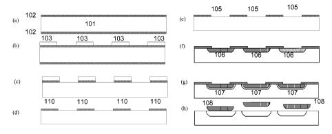
[0080] In a process schematically illustrated in Figures lA and 1B, particles
patterning
precedes the porous layer formation and release of the particles is performed
via
electropolishing. The fabrication may start with obtaining a silicon wafer
101. The surface
of the wafer 101 may be optionally roughened by a treatment, such as KOH
dipping or
reactive-ion etching (RIE). The roughening of the surface may help in removing
or
preventing the formation of the nucleation layer on the surface. A protective
layer 102 may
be then deposited on at least one surface of the wafer 101 to protect the
wafer from
electrochemical etching in HF based solution. The protective layer 102 can be
a material
resistant to electrochemical etching in HF solution. Examples of such
materials include
silicon nitride or photoresist.
[0081] Then the protective layer 102 may be patterned. Figures 1A and 1B
illustrate
patterning of the protective layer by a lithographic technique. As Figures lAc
and 1Bc, a
layer of a resistant material 103 is deposited over the protective layer 102.
The resistant
material may be a material that does not get removed under the conditions, for
which the
protective layer gets removed. One example of such a material is a
photoresist. The
undesired area of the protective layer 102 on the front surface of the wafer
may be removed
13
CA 02685544 2009-10-27
WO 2008/134637
PCT/US2008/061775
as well as the protective layer on the back side on the wafer, see Figures lAc
and 1Bc. The
resistant material 103 may be removed as well, see Figure lAd. The protective
layer may be
patterned is such a way so that the spaces between the patterned areas 110 of
the protective
layer define the shape and dimensions of the fabricated particles.
[0082] In some cases, as illustrated in Figures 1Bd, trenches may be formed in
the spaces 104
between the patterned areas 110 of the protective layer. The trenches may be
formed by, for
example, by a dry etching technique, such as RIE. The depth and shape of
trenches may be
used to define the cross section of the particles perpendicular to the surface
of the substrate
and thus the shape of the particles. The depth and shape of the trenches may
be also to
control mechanical and/or porous properties of the fabricated particle.
[0083] A porous layer 106 may be formed in and around the spaces unprotected
by the
patterned areas 110 of the protective layer, see Figure lAf and 1Bf. To form
the porous layer
106, the wafer may be exposed to a solution that may include HF and optionally
a surfactant,
such as an ethanol, under a DC electrical current, a value of which may be
selected to
generate pores of a desired size. If a nucleation layer 105 is undesirable, a
larger DC current
may be applied prior to applying the DC current corresponding to the desired
pore size, see
Figure lAe.
[0084] The formed porous layer 106 may have two different pore orientations in
the region
unprotected by the patterned areas 110 and in the region of the substrate
under the protective
layer areas 110. The former may have pores oriented perpendicular or
substantially
perpendicular to the surface of the substrate, while the latter may have pores
oriented parallel
to the surface of the substrate or angled to the surface with an angle
substantially different
from 90 .
[0085] The particles 108 or 109 may be released via electropolishing, which
may form a gap
107 underneath the porous layer 106, see Figures lAg,h and 1Bg,h. The
remaining protective
layer may be then removed. The particles may be collected in the solution by a
number of
techniques, including filtration. The particles 109 have a trench formed in
them that may
define their shape and their mechanical and porous properties. For example, a
part of the
particle 109 under the trench may have a pore size and porosity that are
different from a pore
size and porosity at the sides of the particle 109, i.e. non-trench part of
the particle 109.
Example 2. Fabrication of porous silicon particles. Release via formation of
the second
porous layer
[0086] In a process schematically illustrated in Figures 2A and 2B, particles
patterning
precedes a porous layer formation and release of the particles is performed
via a formation of
14
CA 02685544 2009-10-27
WO 2008/134637
PCT/US2008/061775
a second porous layer. The fabrication process may start with obtaining of a
silicon wafer
201. As in the previous protocol, a surface the wafer 201 may roughened by,
for example,
KOH dipping or RIE. As in Example 1, a protective layer 202 may be then
deposited on the
wafer to protect the wafer from electrochemical etching in HF based solution,
see Figure
2Aa. As in Example 1, the protective film 202 may be then patterned using, for
example, a
lithographic technique, see Figures 2Ab,c and 2Bb,c. As in Example 1, the
patterning may
involve deposition of a resistant film 203, see Figures 2Bb and 2Ab. The
undesired area of
the protective film on the front side of the wafer may be removed, as well as
the protective
film on the back side of the wafer 201, see Figure 2Bc and 2Ac. As in Example
1, the
protective layer 202 may be patterned is such a way so that the spaces between
the patterned
areas 210 define the shape and dimensions of the fabricated particles.
[0087] In some cases, as illustrated in Figures 2Bd, trenches 204 may be
formed in the spaces
between the patterned areas 210 of the protective layer. The trenches may be
formed by dry
etching, such as RIE. The depth and shape of trenches may be used to define
the cross
section of the particles perpendicular to the surface of the substrate and
thus the shape of the
particles. The depth and shape of the trenches may be also used to control
mechanical and
porous properties of the formed particles.
[0088] A porous layer 206 may be formed in and around the spaces unprotected
by the
patterned areas 210 of the protective layer, see Figures 2Ae,f and 2Bf. To
form the porous
layer 206, the wafer may be exposed to a solution that may include HF and
optionally a
surfactant under a DC electrical current, a value of which may be selected to
generate pores
of a desired size. If a nucleation layer is undesirable, a larger DC current
may be applied
prior to applying the DC current corresponding to the desired pore size.
[0089] The formed porous layer 206 may have two different pore orientations in
the region
unprotected by the patterned areas 210 and in the region of the substrate
under the protective
layer areas 210. The former may have pores oriented perpendicular or
substantially
perpendicular to the surface of the substrate, while the latter may have pores
oriented parallel
to the surface of the substrate or angled to the surface of the substrate with
an angle
substantially different from 90 .
[0090] After the formation of the porous layer 206, a larger electrical
current may be applied
to form a second porous layer 207 that has a larger porosity than the first
layer, see Figures
2Bf and 2Af. This larger electrical current can be selected to be such that
that the second
CA 02685544 2009-10-27
WO 2008/134637
PCT/US2008/061775
porous layer 207 is fragile enough for mechanical break-down, but still can
hold the particles
in place.
[0091] If the nucleation layer has not been removed earlier, it may be removed
at this stage
by using a dry etching technique, such as RIE. The patterned areas 210 of the
protective film
may be then removed, see Figures 2Ag and 2Bg. The particles kept in the wafer
201 by the
second porous layer 207 can be then chemically modified, if desired.
[0092] The particles 208 or 209 may be released from the wafer 201 in a
solution by breaking
the second porous layer 207, which can be done for example by mechanical means
such as
exposing the wafer to ultrasonic vibrations, see Figures 2Ah and 2Bh. The
particles 209 have
a trench formed in them that may define their shape and their mechanical and
porous
properties. For example, a part of the particle 209 under the trench may have
a pore size and
porosity that are different from a pore size and porosity at the sides of the
particle 209, i.e.
non-trench part of the particle 209.
[0093] The shapes of particles fabricated in Examples 1 and 2 may be
semispherical, bowl,
frustum, etc., depending on the etching condition. For example, for the bowl
shape, a depth
of the bowl can depend on a depth of the trench formed into the particle
patterns prior to
electrochemical wet etching.
Example 3. Fabrication of porous silicon particles
[0094] In a process schematically illustrated in Figure 3, porous layer
formation precedes
particles patterning. The process may start with obtaining a silicon wafer
301. To form a
porous layer 302, the wafer may then exposed to a solution that may include HF
and
optionally surfactant, under a DC electrical current, a value of which may be
selected to
obtain a desired size of pores in the layer 302, see Figure 3a. A larger
electrical current may
be subsequently applied to form a second porous layer 303 in the substrate 301
underneath
the first porous layer. This larger electrical current may be selected so that
the second porous
layer 303 has a larger porosity than the first porous layer 302, see Figure
3b. Preferably, this
larger electrical current is selected to be such that the porous layer 303 is
fragile enough for
mechanical break-down if necessary, but, at the same time, can hold formed
particles in place
within the wafer.
[0095] After the formation of the second porous layer, particles may be
patterned. For
example, one can deposit a photoresist layer onto the porous silicon film 301.
The
photoresist layer may then patterned to define particles. For example, in
Figure 3, patterned
areas 304 of the photoresist layer (Figure 3c) define the particles. The
undesired area of the
porous silicon layer 302, i.e. the areas of the porous layer 302 not covered
by the patterned
16
CA 02685544 2009-10-27
WO 2008/134637
PCT/US2008/061775
areas 304 of the photoresist layer, may be removed by, for example, dry
etching, such as RIE,
see Figure 3d. The patterned areas 304 of the photoresist layer may be then
removed.
[0096] The particles kept in the wafer 301 by the second porous layer 303, see
Figure 3e, can
be then chemically modified, if desired. The particles 306 may be released
from the wafer
301 in a solution by breaking the second porous layer 302, which can be done
for example by
mechanical means, such as exposing the wafer to ultrasonic vibrations, see
Figure 3f.
Example 4. High Yield Fabrication of Porous Silicon Particles I
[0097] The process of Example 3 may be transformed to a multilayer method,
which may
allow for producing a high yield of fabricated particles. The method may start
with obtaining
a silicon wafer 401. The wafer 401 may be then exposed to HF/surfactant
solution, and DC
electrical current may applied for certain time to form a first porous silicon
layer 402, see
Figure 4a. Then a larger electrical current may be applied to form a second
porous layer 403
with larger porosity as a release layer. This larger current may be selected
to be such that the
second porous layer 403 is fragile enough for mechanical break-down, but, at
the same time,
can hold the particles in the wafer 401.
[0098] The steps of forming a stable porous layer, such as the first porous
layer 402, and
forming a breakable release porous layer, such as the second porous layer 403,
may be
repeated to form a periodical layered structure. For example, Figure 4b shows
such a
periodic structure, in which stable porous layers 402 are separated by
breakable release layers
403. Patterning of particles may then be performed.
[0099] For example, a masking layer, such as a metal film, may be deposited on
the top first
porous layer 402. A photoresist layer may be placed on top of the masking
film. In the case
when the metal masking film is not deposited, the photoresist may be placed
directly of the
top first porous layer 402. Then, a lithographic technique may be applied to
pattern the
photoresist layer. As shown in Figure 4c, the patterned photoresist layer may
include
patterned photoresist areas, which may define shape and dimensions of
fabricated particles.
An undesired area of the periodical porous structure, i.e. the area of the
periodical structure
not covered by the patterned photoresist areas 404, may be then removed to
form stacks 406
toped by the patterned photoresist areas 404, see Figure 4d. Then, the
photoresist film and/or
the masking film may be removed from the top of the stacks 406, see Figure 4e,
by using, for
example, piranha solution (1 volume H202 and 2 volumes of H2504). If desired,
particles
405, which are formed from portions of stable porous layers and which are kept
in the stacks
406 by releasable porous layers may then chemically modified. A release of the
particles 405
17
CA 02685544 2009-10-27
WO 2008/134637
PCT/US2008/061775
from the stacks 406 into a solution may be performed by mechanical means, such
as exposing
the wafer 401 with the stacks 406 to ultrasonic vibrations, see Figure 4f.
Example S. High Yield fabrication of porous silicon particles II
[0100] The present example presents an alternative method for a high yield
fabrication of
porous silicon particles. Starting from a silicon wafer 501, a protective
layer may be
deposited on the wafer to protect the wafer from anisotropic etching, such as
Deep RIE. The
protective layer may be, for example, as a silicon dioxide film or a
photoresist film. The
protective film may be patterned to form patterned areas 502 of the protective
layer that
define a cross section shape and dimensions of particles to be fabricated, see
Figure 5a. This
initial patterning of the protective layer may performed similarly to the
patterning of the
protective layer illustrated in Figure 1A (a)-(d).
[0101] An anisotropic etching technique may be then applied to unprotected
areas of the
wafer to form pillars 503 underneath the patterned areas 502 of the protective
film, see Figure
5b. The protective film 502 on the top of the pillars 503 may be then removed.
Then, a
second protective layer 504 may be deposited over the pillars 503 and in the
etched areas 508
between the pillars 503, see Figure Sc. The second protective layer 504 can be
such so that it
can protect the wafer from electrochemical etching in HF based solution. For
example, the
second protective layer 504 can be a silicon nitride film or a photoresist
film. The tops of the
pillars 503 may be then exposed by removing portions of the second protective
layer 504 by,
for example, etching or planation. Preferably, after such removal, the second
protective layer
504 remains intact on the sides and at the bottom of the etched areas 508, see
Figures 5d.
[0102] After that, the wafer with the patterned pillars may be exposed to HF-
based solution
under applied DC electrical current to form a first porous layer 505, which is
a stable porous
layer from which the particles may be formed. The applied DC current may be
selected to
form pores with a size desired in the particle. After that, a larger
electrical current may be
applied to form a second porous layer 506, which is a release porous layer
with a larger
porosity than the first porous layer 505. This larger electrical current may
be selected to be
such so that the release porous layer is, on one hand, fragile enough for
mechanical break-
down, and, on the other, it is strong enough to hold the particles in place
before the release.
The steps of formation a stable porous layer, such as the layer 505 and
formation of a release
layer, such as a layer 506 may be repeated a desired number of times to form a
periodical
layered structure in the pillars 503. For example, Figure 5(e) shows a
periodical structure
509 formed by interchanging stable porous layers 505 and release porous layers
506. Upon
18
CA 02685544 2009-10-27
WO 2008/134637
PCT/US2008/061775
the formation of the periodic stack structure 509, the remaining second
protective layer 504
may be removed, see Figure 5f.
[0103] If desired, particles 507, which are formed from portions of stable
porous layers 505
and which are kept in the periodic stack structures 509 by releasable porous
layers 506, may
then chemically modified. A release of the particles 507 from the stacks 509
into a solution
may be performed by mechanical means, such as exposing the wafer 501 with the
stacks 509
to ultrasonic vibrations, see Figure 5g.
[0104] In the above method, the step of forming large porosity release layers
may be replaced
by electropolishing. In this case, the formed periodic structures may include
interchanging
stable porous layers and gaps formed by electropolishing, instead of the
release porous layer.
The stable porous layers may be hold intact with the wafer by the remaining
second
protective layer 504. In such a case, the release of the particles formed from
the stable
porous layers may be performed by removing the remaining second protective
layer. Prior to
the release, the particles may be chemically modified while still intact with
the wafer.
Surface modification protocols
[0105] Below are provided exemplary protocols, which may be used for surface
modification
of silicon particles by oxidation, silanization and attaching targeting
moieties, such as
antibodies.
Oxidation of Silicon microparticles
[0106] Silicon microparticles in IPA can be dried in a glass beaker kept on a
hot plate (80-
90 C). Silicon particles can be oxidized in piranha (1 volume H202 and 2
volumes of
H2504). The particles can be sonicated after H202 addition and then acid can
be added. The
suspension can be heated to 100-110 C for 2 hours with intermittent sonication
to disperse
the particles. The suspension can be then washed in DI water till the pH of
the suspension is
about 5.5 ¨ 6. Particles can be then transferred to appropriate buffer, IPA
(isopropyl alcohol)
or stored in water and refrigerated till further use.
Silanization
[0107] Oxidation. Prior to
the silanization process, the oxidized particles can be
hydroxylated in 1.5 M HNO3 acid for approximately 1.5 hours (room
temperature). Particles
can be washed 3-5 times in DI water (washing can include suspending in water
and
centrifuging, followed by the removal of supernatant and the repeating of the
procedure).
[0108] APTES Treatment. The particles can be suspended in IPA (isopropyl
alcohol) by
washing them in IPA twice. Then the particles can be suspended in IPA solution
containing
0.5% (v/v) of APTES (3-aminopropyltriethoxysilane) for 45 minutes at room
temperature.
19
CA 02685544 2009-10-27
WO 2008/134637
PCT/US2008/061775
The particles can be then washed with IPA 4-6 times by centrifugation and
stored in IPA
refrigerated. Alternatively, the particles can be aliquoted, dried and stored
under vacuum and
desiccant till further use.
[0109] MPTMS Treatment. The particles can be hydroxylated in HNO3 using the
same
procedure as above. After the washes with water and IPA, the particles can be
silanized with
MPTMS (3-mercaptopropyltrimethoxysilane) 0.5% v/v and 0.5% v/v in IPA for 4
hours. The
particles can be then washed with IPA 4-6 times, and then stored in IPA
refrigerated or
aliquoted, dried, and stored under vacuum and desiccant.
[0110] Conjugation of Antibodies. Microparticles can be modified with APTES
and/or
MPTMS as described above. Sulfo-SMCC, a water soluble analog of succinimidyl 4-
N-
maleimidomethyl cyclohexane-l-carboxylate (SMCC) crosslinker, can be used to
crosslink
the particles with the anti-VEGFR2 antibody. The total number of particles
used for
conjugating both APTES and MPTMS particles with the anti-VEGFR2 can be about
7.03 X
106. The particles can be washed and centrifuged in phosphate buffer
containing 0.5% Triton
X-100 6 times followed by 4 washes in plain phosphate buffer and then read on
the plate
reader.
[0111] Immobilization of antibodies, such as IgG, EGFR, VEGFR, to nanoporous
silicon
particles via a chemical scaffold by surface sialinization followed by
subsequent coupling
methods involving readily available protein crosslinking agents capable of
covalently linking
these antibodies has been experimentally demonstrated.
Surface Modification with APTES
[0112] In an exemplary surface modification, porous silicon particles can be
hydroxylated in
1.5M HNO3 for 1 hr. Amine groups are introduced on the surface by silanization
with a
solution comprising 0.5% v/v 3-aminopropyltriethoxysilane (APTES) in
isopropanol (IPA)
for 30 min at room temperature. Thiol groups can be coated on the surface
using 0.5% v/v 3-
mercaptopropyltrimethoxysilane (MPTMS) and 0.5%v/v H20 in IPA. APTES-coated
and
MPTMS-coated particles can be suspended in phosphate-buffered ssline (PBS) and
reacted
with the crosslinker 1mM N-succinimidyl-S-acetylthioacetate (SATA), 1 mM
sulfosuccinimidyl 4-(N-maleimidomethyl)cyclohexane-1-carboxylate (Sulfo-SMCC),
1mM
N-Succinimidy1[4-iodoacetyl]aminobenzoate (Sulfo-SIAB), or 1mM succinimidyl
64342-
pyridyldithio]-propionamido)hexanoate (SPDP) for lh at room temperature. Then
the
antibodies can be bioconjugated on the particles.
CA 02685544 2009-10-27
WO 2008/134637
PCT/US2008/061775
Example 6: Fabrication of "Large Pore" Silicon Particles
[0113] Figure 6 shows a scanning electron image of a 1.2 p.m silicon porous
particle
fabricated as follows. Heavily doped p++ type (100) wafer with resistivity of
0.005 ohm-cm
(Silicon Quest Inc) was used as the substrate. A 200 nm layer of silicon
nitride was deposited
by Low Pressure Chemical Vapor Deposition (LPCVD) System. Standard
photolithography
was used to pattern the 1 p.m circular particle patterns using EVG 620 aligner
(vacuum
contact). The silicon nitride was then selectively removed by reactive ion
etching (RIE). The
silicon nitride on the back side of the wafer was removed by RIE. 300 nm
silicon trenches
were etched into silicon in exposed particle patterns. The photoresist was
removed with
piranha (H2SO4:H202=3:1 by volume). Aluminum film was coated on the backside
of the
wafer. The wafer was then placed in a home-made Teflon cell for
electrochemical etching.
The nanopores were formed in the mixture of hydrofluoric acid (HF) and Ethanol
(3:7 v/v)
with applied current density of 80 mA/cm2 for 25 second. A release high
porosity layer was
formed by applying the current density of 400 mA/cm2 for 6 second. After
removing the
nitride layer by HF, particles were released in IPA by exposure to ultrasound
for 1 minute.
The IPA containing porous silicon particles was collected and stored.
[0114] The morphology of the silicon particles was determined using LEO 1530
scanning
electron microscopy. Particles in IPA were directly placed on aluminum SEM
sample stage
and dried. The SEM stages with particles are loaded into LEO 1530 sample
chamber. The
acceleration voltage of electron beam is 10 kV, and working distance is about
5 mm.
[0115] The SEM image in Figure 6 shows a bottom view, i.e. a view of a side,
which was
away from a front surface of the wafer during the fabrication, of a particle
having a circular
(1.2 p.m in diameter) shape parallel to the surface of the wafer. The overall
3 dimensional
shape of the particle in Figure 6 is semispherical. The image in Figure 6
shows regions 601
and 602, which correspond to pores parallel or angled to the surface and pores
perpendicular
to the surface, respectively. The pore size in the center of particle is about
30 nm. The
resulting particles are bigger than the original patterns because the porous
layer may
penetrate beneath and into the protected area of the substrate during
electrochemical etching.
Example 7. Fabrication of Oval Shaped "Large Pore" Silicon Particles
[0116] Figure 7 shows an SEM image of a silicon particle having an oval cross
section. The
particle was fabricated as follows. Heavily doped p++ type (100) wafer with
resistivity of
0.005 ohm-cm (Silicon Quest Inc) was used as the substrate. A 200 nm layer of
silicon
nitride was deposited by Low Pressure Chemical Vapor Deposition (LPCVD)
System.
Standard photolithography was used to pattern the 2 p.m oval shaped particles
using EVG 620
21
CA 02685544 2009-10-27
WO 2008/134637
PCT/US2008/061775
aligner. The nitride was then selectively removed by reactive ion etching
(RIE). The silicon
nitride on the back side of the wafer was removed by RIE. 600nm silicon
trenches are etched
into silicon in exposed particle patterns. The photoresist was removed with
piranha
(H2SO4:H202=3:1 by volume). The wafer was then placed in a home-made Teflon
cell for
electrochemical etching. The etching solution was a mixture of hydrofluoric
acid (HF) and
ethanol (3:7 v/v). A high density electrical current of 400 mA/cm2 was applied
for 1 second
to remove a nucleation layer. Then the nanopores were formed with applied
current density
of 80 mA/cm2 for 25 second. A high porosity release layer was formed by
applying a current
density of 400 mA/cm2 for 6 second. After removing the nitride layer by HF,
particles were
released in IPA by ultrasound for 1 minute. The IPA solution containing porous
silicon
particles was collected and stored. A drop of the IPA solution containing the
fabricated
particles was directly placed on aluminum SEM sample stage and dried. The SEM
image was
measured using a LEO 1530 scanning electron microscope. The acceleration
voltage of
electron beam is 10 kV, and working distance is about 5 mm. The SEM image in
Fig. 7
shows the top view of the resulting particle. The particle has a region 701,
in which pores are
parallel or angled to the surface, and a region 702, in which pores are
perpendicular to the
surface.
Example 8: Fabrication of "Small Pore" Silicon Particles
[0117] Figure 8 is an SEM image showing 3.1 p.m particles that have a
semispherical shape.
The particles were fabricated as follows. Heavily doped p++ type (100) wafer
with resistivity
of 0.005 ohm-cm (Silicon Quest Inc) was used as a substrate. A 200-350 nm
layer of silicon
nitride was deposited on the substrate by Low Pressure Chemical Vapor
Deposition
(LPCVD) System. Photolithography was used to pattern the 2 p.m circular
particle patterns.
The nitride was then selectively removed by reactive ion etching (RIE). The
silicon nitride
on the back side of the wafer was removed by RIE. The photoresist was removed
with
piranha (H2SO4:H202=3:1 by volume). The wafer was then placed in a home-made
Teflon
cell for electrochemical etching. The nanopores were formed in a mixture of
hydrofluoric
acid (HF) and Ethanol (1:1 v/v) with a current density of 6 mA/cm2 applied for
1 min 45
second. A high porosity release layer was formed by applying a higher current
density of 320
mA/cm2 for 6 second in the mixture of hydrofluoric acid (HF) and Ethanol (2:5
v/v). After
removing the nitride layer by HF, the particles were released by exposing the
substrate to
ultrasonic vibrations for 1 minute. A drop containing particles in IPA was
directly placed on
an aluminum SEM sample stage and dried. The SEM image was measured using a LEO
1530
scanning electron microscope. The acceleration voltage of electron beam is 10
kV, and
22
CA 02685544 2009-10-27
WO 2008/134637
PCT/US2008/061775
working distance is about 5mm. The SEM image in Figure 8 shows the fabricated
particles.
The inset demonstrates that the fabricated particle have a pore size of less
than 10 nm.
Example 9: Fabrication of "Large Pore" Silicon Particles
[0118] Figure 10 shows an SEM image of 3.2 p.m silicon particles with 500 nm
trench. The
particles were fabricated as follows. Heavily doped p++ type (100) wafer with
resistivity of
0.005 ohm-cm (Silicon Quest Inc) was used as a substrate. A 100 nm layer of
low stress
silicon nitride was deposited on the substrate by Low Pressure Chemical Vapor
Deposition
(LPCVD) System. Standard photolithography was used to pattern the 2 p.m
circular particle
patterns using EVG 620 aligner. The nitride was then selectively removed by
reactive ion
etching (RIE). The silicon nitride on the back side of the wafer was removed
by RIE. 500 nm
silicon trenches were etched into silicon on the exposed particle patterns by
RIE. The
photoresist was removed with piranha (H2504:H202 = 3:1 by volume). The wafer
was then
placed in a home-made Teflon cell for electrochemical etching. The nanopores
were formed
in a mixture of hydrofluoric acid (HF) and Ethanol (1:3 v/v) with a current
density of 16
mA/cm2 applied for 105 second. A higher porosity release layer was formed by
applying a
current density of 220 mA/cm2 for 6 second. After removing the nitride layer
by HF, the
particles were released in IPA by exposing the wafer to ultrasonic vibration
for 1 minute.
The IPA solution containing porous silicon particles was collected and stored.
[0119] A drop containing the particles in IPA was directly placed on an
aluminum SEM
sample stage and dried. The SEM image was measured using a LEO 1530 scanning
electron
microscope. The acceleration voltage of electron beam was 10 kV, and working
distance is
about 5 mm. The SEM image in Fig. 10 shows the resulting bowl shaped
particles. The
particles have about 30 nm pores on the bottom of the bowl and smaller pores
on the sides.
Example 10: Fabrication of "Large Pore" Silicon Particles with Deep Trenches
Etching
[0120] Figure 11 shows an SEM image of fabricated silicon particles with ¨1.5
p.m deep
trench formed by silicon etching. The particles were fabricated as follows.
[0121] Heavily doped p++ type (100) wafer with resistivity of 0.005 ohm-cm
(Silicon Quest
Inc) was used as a substrate. A 100 nm layer of low stress silicon nitride was
deposited on
the substrate by Low Pressure Chemical Vapor Deposition (LPCVD) System.
Standard
photolithography was used to pattern the 2 p.m circular particle patterns
using EVG 620
aligner. The nitride was then selectively removed by reactive ion etching
(RIE). The silicon
nitride on the back side of the wafer was removed by RIE. The silicon trenches
of 1500 nm
were etched into silicon on the exposed particle patterns. The photoresist was
removed with
piranha (H2SO4:H202=3:1 by volume). The wafer was then placed in a home-made
Teflon
23
CA 02685544 2009-10-27
WO 2008/134637
PCT/US2008/061775
cell for electrochemical etching. The nanopores were formed in a mixture of
hydrofluoric
acid (HF) and Ethanol (1:3 v/v) by applying a current density of 16 mA/cm2 for
105 second.
A high porosity release layer was formed by applying a current density of 220
mA/cm2 for 6
second. After removing the nitride layer by HF, the particles were released in
IPA by
exposing the wafer to ultrasonic vibrations for 1 minute. The IPA solution
containing porous
silicon particles was collected and stored.
[0122] A drop containing the particles in IPA was directly placed on an
aluminum SEM
sample stage and dried. The SEM image was measured using a LEO 1530 scanning
electron
microscope. The acceleration voltage of electron beam is 10 kV, and working
distance is
about 5 mm. The SEM image in Fig. 11 shows the resulting bullet shaped
particles. The tip
1101 of the bullet has pores of about 30 nm, while the body 1102 of the bullet
has smaller
pores.
Example 11: Fabrication of "Large Pore" Silicon Particles with a nucleation
layer removed
by RIE
[0123] Figure 12 shows SEM cross-section images of fabricated 3.2 p.m silicon
particles with
500 nm silicon trench etching and: left: with nucleation layer; right:
nucleation layer removed
by RIE. The particles were fabricated as follows. Heavily doped p++ type (100)
wafer with
resistivity of 0.005 ohm-cm (Silicon Quest Inc) was used as a substrate. A 100
nm layer of
low stress silicon nitride was deposited on the substrate by Low Pressure
Chemical Vapor
Deposition (LPCVD) System. Standard photolithography was used to pattern the 2
p.m
circular particle patterns using EVG 620 aligner. The nitride was then
selectively removed
by reactive ion etching (RIE). The silicon nitride on the back side of the
wafer was also
removed by RIE. 500 nm silicon trenches were etched into silicon on the
exposed particle
patterns. The photoresist was removed with piranha (H2SO4:H202=3:1 by volume).
The wafer
was then placed in a home-made Teflon cell for electrochemical etching. The
nanopores
were formed in a mixture of hydrofluoric acid (HF) and Ethanol (1:3 v/v) by
applying a
current density of 16 mA/cm2 for 105 second. A high porosity release layer was
formed by
applying a current density of 220 mA/cm2 for 6 second. Then a short time CF4
RIE was
applied to remove the nucleation layer.
[0124] For the cross-section study, the particles were not released from the
wafer. Instead,
after removing the nitride layer by HF, the wafer was cleaved, and mounded on
a 45 degree
aluminum SEM sample stage. The SEM image was measured using a LEO 1530
scanning
electron microscope. The acceleration voltage of electron beam is 10 kV, and
working
distance is about 5 mm. The SEM image in Fig. 12 compares the cross-section of
resulting
24
CA 02685544 2009-10-27
WO 2008/134637
PCT/US2008/061775
particles with nucleation layer and particles after removed nucleation layer.
The particles
with nucleation layer have less than 10 nm pores in the top area 1201, and
about 30 nm pores
underneath the nucleation layer 1202, while the particles without nucleation
layer have about
30 nm pores in both the top area 1203 and the area 1204 beneath the top.
Example 12: Fabrication of "Large Pore" Silicon Particles with two different
porosity along
pore direction
[0125] Figure 13 shows an SEM image a porous particle having two different
porous regions
along pore direction. The particle was fabricated as follows: heavily doped
p++ type (100)
wafer with resistivity of 0.005 ohm-cm (Silicon Quest Inc) was used as a
substrate. A 100
nm layer of low stress silicon nitride was deposited on the substrate by Low
Pressure
Chemical Vapor Deposition (LPCVD) System. Standard photolithography was used
to
pattern the 2 um circular particle patterns using EVG 620 aligner. The nitride
was then
selectively removed by reactive ion etching (RIE). The silicon nitride on the
back side of the
wafer was also removed by RIE. 500 nm silicon trenches are etched into silicon
on exposed
particle patterns. The photoresist is removed with piranha (H2SO4:H202=3:1 by
volume).
The wafer was then placed in a home-made Teflon cell for electrochemical
etching. The
nanopores were formed in a mixture of hydrofluoric acid (HF) and Ethanol (1:3
v/v) by
applying a current density of 16mA/cm2 for 50 seconds and 37 mA/cm2 for 22
seconds.
[0126] For the cross-section study, the particles were not released from the
wafer. Instead,
after removing the nitride layer by HF, the wafer was cleaved, and mounded on
a 45 degree
aluminum SEM sample stage. The SEM image was measured using a LEO 1530
scanning
electron microscope. The acceleration voltage of electron beam is 10 kV, and
working
distance is about 5mm. The SEM image in Fig. 13 shows the resulting particles
with two
different porosity regions 1301 and 1302 along a longitudinal direction
besides a nucleation
layer 1303. Pores in both regions 1301 and 1302 are perpendicular to the
surface. The
region 1301 has larger porosity than the region 1302.
Example 13: Fabrication of porous silicon films
[0127] Figure 9 shows images of two porous silicon films one with a nucleation
layer
(Figures 9A-B) and one without a nucleation layer (Figure 9C). The films were
fabricated as
follows:
[0128] Heavily doped p++ type (100) wafer with resistivity of 0.005 ohm-cm
(Silicon Quest
Inc) was used as a substrate. The wafer was then placed in a home-made Teflon
cell for
electrochemical etching. The etching solution is a mixture of hydrofluoric
acid (HF) and
Ethanol (2:5 v/v). A high density electrical current of 320mA/cm2 was applied
for 1 second
CA 02685544 2015-11-12
WO 2008/134637
PCT/US200S/061775
1
to remove nucleation layer. The nanopores were formed in with applied current
density of 80
rnA/cm2 for 25 second. Although the foregoing refers to particular preferred
embodiments, it
will be understood that the present invention is not so limited. It will occur
to those of
ordinary skill in the art that various modifications may be made to the
disclosed embodiments,
[01291 Some specific embodiments include the following. A method of
fabricating
nanoporous silicon particles, comprising: providing a silicon substrate
comprising a surface;
forming a porous layer on said surface; lithographically patterning a
plurality of particles
on said substrate, said particles comprising said porous layer; and releasing
said particles from
the resulting substrate containing patterned porous particles. In
some embodiments,
lithographic patterning is performed before forming said porous area on said
surface.
101301 In some embodiments, releasing said particles comprises mechanically
releasing said
particles from the lithographically patterned porous particles. In some
embodiments, wherein
forming said porous layer comprises forming a first porous layer and forming a
second
porous layer, wherein the porosity of said second layer is greater than that
of the first layer.
In some embodiments, a protective layer is applied on said substrate, In
certain
embodiments, the protective layer comprises silicon nitride or a photoresist
film. In some
embodiments, releasing said particles from said substrate comprises removing
the undesired
area of said protective layer.
10131] In accordance with some embodiments of an above-described method,
patterning
comprises defining a predetermined shape for the resulting particles. In some
embodiments,
said predetermined shape is selected from the group consisting of spherical,
square,
rectangular, ellipse, disk and semi-spherical,
[0132] In accordance with some embodiments, forming of said porous layer
comprises tuning
the properties of the resulting silicon particles. In certain embodiments,
said properties
comprise the porosity, pore size and pore profile of said resulting silicon
particles. In certain
embodiments, said forming of said porous layer comprises electrochemically
treating said
substrate. In
certain embodiments, wherein electrochemically treating said substrate
comprises treatment with a solution containing hydrofluoric acid and a
surfactant. In certain
embodiments, tuning the properties of said silicon particles comprises
selecting a
concentration of said solution, selecting an electrical current, selecting an
etching time, and
selecting a doped silicon substrate to provide silicon particles having
predetermined
properties.
26
CA 02685544 2015-11-12
WO 2008/134637 PCT/US2008/061775
[0133] In accordance with some embodiments of an above-described method, said
silicon
particles comprise an outer surface and a porous interior, and said method
further comprises
functionalizing at least a portion of said particles, In certain
embodiments, said
functionalizing comprises modifying at least said outer surface of said
particles by
application of at least one treatment selected from the group consisting of
chemicals,
biochemicals, polymers, oxidation, plasma treatment, metal or metal ion
coating, CVD film
coating, atomic layer deposition, evaporated films, sputtered films and ion
implants. In
certain embodiments, applying a sacrificial polymer to the porous interior of
said particles
prior to said functionalizing. in certain embodiments, said functionalizing is
performed prior
to said releasing of said silicon particles.
[0134] Also provided in accordance with embodiments of the present invention
is the product
of the method of any of the above-described methods, In certain embodiments,
the product
comprises about 1-3 micron silicon-based nanoporous particles.
[0135] Without further elaboration, it is believed that one skilled in the art
can, using the
description herein, utilize the present invention to its fullest extent. The
embodiments
described herein are to be construed as illustrative and not as constraining
the remainder of
the disclosure in any way whatsoever. While the preferred embodiments of the
invention
have been shown and described, many variations and modifications thereof can
be made by
one skilled in the art. Accordingly, the scope of protection is not limited by
the description
set out above, but is only limited by the claims, including all equivalents of
the subject
matter of the claims.
_
27