Note: Descriptions are shown in the official language in which they were submitted.
CA 02685682 2009-10-29
WO 2008/137299 PCT/US2008/061046
DUAL FILM LIGHT GUIDE FOR ILLUMINATING DISPLAYS
BACKGROUND
Field of the Invention
[0001] The present invention relates generally to frontlit displays, such as
LCD
displays, and particularly to dual film configurations of light guides for
frontlit displays.
Description of the Related TechnoloU
[0002] Microelectromechanical systems (MEMS) include micro mechanical
elements, actuators, and electronics. Micromechanical elements may be created
using
deposition, etching, and/or other micromachining processes that etch away
parts of substrates
and/or deposited material layers or that add layers to form electrical and
electromechanical
devices. One type of MEMS device is called an interferometric modulator. As
used herein,
the term interferometric modulator or interferometric light modulator refers
to a device that
selectively absorbs and/or reflects light using the principles of optical
interference. In certain
embodiments, an interferometric modulator may comprise a pair of conductive
plates, one or
both of which may be transparent and/or reflective in whole or part and
capable of relative
motion upon application of an appropriate electrical signal. In a particular
embodiment, one
plate may comprise a stationary layer deposited on a substrate and the other
plate may
comprise a metallic membrane separated from the stationary layer by an air
gap. As
described herein in more detail, the position of one plate in relation to
another can change the
optical interference of light incident on the interferometric modulator. Such
devices have a
wide range of applications, and it would be beneficial in the art to utilize
and/or modify the
characteristics of these types of devices so that their features can be
exploited in improving
existing products and creating new products that have not yet been developed.
SUMMARY
[0003] Various embodiments described herein comprise light guides for
distributing light across an array of display elements. The light guide may
include surface
relief features to turn light propagating in a light guide onto the array of
display elements.
-1-
CA 02685682 2009-10-29
WO 2008/137299 PCT/US2008/061046
The surface relief features may comprise facets that reflect light. To protect
these facets, the
facets are embedded within the light guide. Other embodiments are also
disclosed.
[0004] One embodiment of the invention comprises a light guide comprising an
upper portion having top and bottom surfaces and a lower portion having top
and bottom
surfaces. The bottom surface of the upper portion is contoured. The top
surface of the lower
portion is also contoured. The upper portion is disposed over the lower
portion such that the
contoured bottom surface of the upper portion and the contoured top surface of
the lower
portion form cavities between the upper portion and the lower portion.
[0005] Another embodiment of the invention comprises a light guide comprising
a cover layer having top and bottom surfaces, a film having top and bottom
surfaces wherein
the top surface of the film is contoured, and a light guide plate having top
and bottom
surfaces. The cover layer is disposed over the film such that the bottom
surface of the cover
layer and the top contoured surface of the film form cavities between the
cover layer and the
film. The film is disposed between the cover layer and the light guide plate.
[0006] Another embodiment of the invention comprises a light guide comprising
a cover layer having a planar surface, a film having first and second
surfaces, and a light
guide plate having top and bottom planar surfaces. The first surface of the
film comprises a
plurality of concave surface relief features and the second surface of the
film is planar. The
film is disposed on the light guide plate such that the planar second surface
is adjacent the
light guide plate and the concave surface relief features of said first
surface face away from
the light guide plate. The cover layer is disposed adjacent the film such that
the planar
surface of the cover layer and the concave surface features of the film form
cavities between
the cover layer and the film.
[0007] Another embodiment of the invention comprises a light guide comprising
a first means for guiding light and a second mean for guiding light. The first
and second light
guiding means have respective means for mating the first and second light
guiding means
together. The mating means for both the first and second light guiding means
is contoured
such that when the first and second light guiding means are mated together.
The means for
reflecting light are formed therebetween.
-2-
CA 02685682 2009-10-29
WO 2008/137299 PCT/US2008/061046
[0008] Another embodiment of the invention comprises a light guide comprising
a first means for guiding light, a second means for guiding light, and means
for covering the
second light guiding mean. The covering means is disposed such that the second
light
guiding means is between the covering means and the first light guiding means.
The second
light guiding means and the covering means have respective means for mating
the second
light guiding means and the covering means together. The mating means for the
second light
guiding means is contoured such that when the second light guiding means and
the covering
means are mated together, means for reflecting light are formed therebetween.
BRIEF DESCRIPTION OF THE DRAWINGS
[0009] FIG. 1 is an isometric view depicting a portion of one embodiment of an
interferometric modulator display in which a movable reflective layer of a
first
interferometric modulator is in a relaxed position and a movable reflective
layer of a second
interferometric modulator is in an actuated position.
[0010] FIG. 2 is a system block diagram illustrating one embodiment of an
electronic device incorporating a 3x3 interferometric modulator display.
[0011] FIG. 3 is a diagram of movable mirror position versus applied voltage
for
one exemplary embodiment of an interferometric modulator of FIG. 1.
[0012] FIG. 4 is an illustration of a set of row and column voltages that may
be
used to drive an interferometric modulator display.
[0013] FIG. 5A illustrates one exemplary frame of display data in the 3x3
interferometric modulator display of FIG. 2.
[0014] FIG. 5B illustrates one exemplary timing diagram for row and column
signals that may be used to write the frame of FIG. 5A.
[0015] FIGS. 6A and 6B are system block diagrams illustrating an embodiment of
a visual display device comprising a plurality of interferometric modulators.
[0016] FIG. 7A is a cross section of the device of FIG. 1.
[0017] FIG. 7B is a cross section of an alternative embodiment of an
interferometric modulator.
-3-
CA 02685682 2009-10-29
WO 2008/137299 PCT/US2008/061046
[0018] FIG. 7C is a cross section of another alternative embodiment of an
interferometric modulator.
I0019] FIG. 7D is a cross section of yet another alternative embodiment of an
interferometric modulator.
[0020] FIG. 7E is a cross section of an additional alternative embodiment of
an
interferometric modulator.
[0021] FIG. 8 depicts a front light guide unit for use in a flat panel display
comprising a linear light source and a front light guide panel.
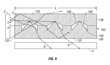
j0022] FIG. 9 depicts a frontlit display comprising a reflective display
panel, a
dual film front light guide panel having embedded surface features and a light
source.
[0023] FIG. 10 depicts the top and bottom films of the dual film light guide
of
FIG. 9.
I0024] FIG. 11 depicts light rays from the display panel propagating through
the
light guide of FIG. 9.
[00251 FIG. 12 depicts light rays from ambient light propagating through the
light
guide to the display panel.
[0026] FIG. 13 depicts an alternative embodiment of a front light guide
wherein
the distance between surface features varies across the length of the light
guide.
[0027] FIG. 14 depicts an alternative embodiment of a front light guide having
embedded surface features.
[0028] FIG. 15 depicts an alternative embodiment of a frontlit display
comprising
a reflective display panel, a front light guide panel having embedded surface
features and a
light source.
[0029] FIG. 16 depicts an alternative embodiment of a front light guide having
embedded surface features.
[0030] FIG. 17 depicts light rays incident on one of the embedded surface
features
of the front light guide of FIG. 16.
[0031] FIG. 18 depicts an alternative embodiment of a front light guide having
embedded surface features with a reflective coating.
-4-
CA 02685682 2009-10-29
WO 2008/137299 PCT/US2008/061046
[0032] FIG. 19 depicts a detailed view of a portion of an alternative
embodiment
of a front light guide showing multifaceted embedded surface features.
100331 FIG. 20 depicts a detailed view of a portion of an alternative
embodiment
of a front light guide showing embedded surface features with curved facets.
[0034] FIG. 21 depicts an alternative embodiment a frontlit display comprising
a
reflective display panel and a front light guide panel having embedded surface
features,
wherein the embedded surface features are disposed on a side of a film facing
the light guide
panel.
[0035] FIG. 22 depicts an alternative embodiment of a frontlit display similar
to
that of FIG. 21 wherein the embedded surface features have vertical walls.
DETAILED DESCRIPTION OF CERTAIN PREFERRED EMBODIMENTS
[0036] The following detailed description is directed to certain specific
embodiments of the invention. However, the invention can be embodied in a
multitude of
different ways. In this description, reference is made to the drawings wherein
like parts are
designated with like numerals throughout.
[0037] In various embodiments described herein, an edge illuminated front
light
guide panel includes a plurality of embedded surface features. The embedded
surface relief
features may form f llable gaps or cavities such as air pockets within the
light guide panel.
Light injected into an edge of the light guide propagates though the light
guide until it strikes
an air/light guide material interface at one on the air pockets. The light is
then turned by total
internal reflection through a large angle such that it exits an output face
disposed in front of a
display panel. To create air pockets, a pair of guide portions have contoured
surfaces that are
contacted to each other. Other embodiments are also disclosed herein.
[0038] As will be apparent from the following description, the embodiments may
be implemented in any device that is configured to display an image, whether
in motion (e.g.,
video) or stationary (e.g., still image), and whether textual or pictorial.
More particularly, it
is contemplated that the embodiments may be implemented in or associated with
a variety of
electronic devices such as, but not limited to, mobile telephones, wireless
devices, personal
data assistants (PDAs), hand-held or portable computers, GPS
receivers/navigators, cameras,
-5-
CA 02685682 2009-10-29
WO 2008/137299 PCT/US2008/061046
MP3 players, camcorders, game consoles, wrist watches, clocks, calculators,
television
monitors, flat panel displays, computer monitors, auto displays (e.g.,
odometer display, etc.),
cockpit controls and/or displays, display of camera views (e.g., display of a
rear view camera
in a vehicle), electronic photographs, electronic billboards or signs,
projectors, architectural
structures, packaging, and aesthetic structures (e.g., display of images on a
piece of jewelry).
[0039] The display device, such as, e.g., interferometric modulating MEMS
devices, LCDs, etc., may include a light source that is configured to light an
array of display
elements to an appropriate level for viewing. In combination with the light
source, a light
guide may be coupled to the array of display elements proximate the light
source to distribute
light across the array of display elements. Light guides may be positioned in
various
orientations with respect to the display elements, such as behind the display
elements, e.g., a
backlight, or in front of the display elements, e.g., a frontlight. In the
systems and methods
described herein, a front light guide panel is disposed in front of the array
of display elements
to deliver uniform illumination from an artificial light source to the array
of display elements
while allowing for the option of illumination from ambient lighting via a
reflective layer in
the display elements.
[0040] One interferometric modulator display embodiment comprising an
interferometric MEMS display element is illustrated in Figure 1. In these
devices, the pixels
are in either a bright or dark state. In the bright ("on" or "open") state,
the display element
reflects a large portion of incident visible light to a user. When in the dark
("offl' or
"closed") state, the display element reflects little incident visible light to
the user. Depending
on the embodiment, the light reflectance properties of the "on" and "off'
states may be
reversed. MEMS pixels can be configured to reflect predominantly at selected
colors,
allowing for a color display in addition to black and white.
[0041] Figure 1 is an isometric view depicting two adjacent pixels in a series
of
pixels of a visual display, wherein each pixel comprises a MEMS
interferometric modulator.
In some embodiments, an interferometric modulator display comprises a
row/column array of
these interferometric modulators. Each interferometric modulator includes a
pair of
reflective layers positioned at a variable and controllable distance from each
other to form a
resonant optical gap with at least one variable dimension. In one embodiment,
one of the
-6-
CA 02685682 2009-10-29
WO 2008/137299 PCT/US2008/061046
reflective layers may be moved between two positions. In the first position,
referred to herein
as the relaxed position, the movable reflective layer is positioned at a
relatively large distance
from a fixed partially reflective layer. In the second position, referred to
herein as the
actuated position, the movable reflective layer is positioned more closely
adjacent to the
partially reflective layer. Incident light that reflects from the two layers
interferes
constructively or destructively depending on the position of the movable
reflective layer,
producing either an overall reflective or non-reflective state for each pixel.
[0042] The depicted portion of the pixel array in Figure 1 includes two
adjacent
interferometric modulators 12a and 12b. In the interferometric modulator 12a
on the left, a
movable reflective layer 14a is illustrated in a relaxed position at a
predetermined distance
from an optical stack 16a, which includes a partially reflective layer. In the
interferometric
modulator 12b on the right, the movable reflective layer 14b is illustrated in
an actuated
position adjacent to the optical stack 16b.
[00431 The optical stacks 16a and 16b (collectively referred to as optical
stack
16), as referenced herein, typically comprise several fused layers, which can
include an
electrode layer, such as indium tin oxide (ITO), a partially reflective layer,
such as chromium,
and a transparent dielectric. The optical stack 16 is thus electrically
conductive, partially
transparent, and partially reflective, and may be fabricated, for example, by
depositing one or
more of the above layers onto a transparent substrate 20. The partially
reflective layer can be
formed from a variety of materials that are partially reflective such as
various metals,
semiconductors, and dielectrics. The partially reflective layer can be formed
of one or more
layers of materials, and each of the layers can be formed of a single material
or a combination
of materials.
[0044] In some embodiments, the layers of the optical stack 16 are patterned
into
parallel strips, and may form row electrodes in a display device as described
further below.
The movable reflective layers 14a, 14b may be formed as a series of parallel
strips of a
deposited metal layer or layers (orthogonal to the row electrodes of 16a, 16b)
deposited on
top of posts 18 and an intervening sacrificial material deposited between the
posts 18. When
the sacrificial material is etched away, the movable reflective layers 14a,
14b are separated
from the optical stacks 16a, 16b by a defined gap 19. A highly conductive and
reflective
-7-
CA 02685682 2009-10-29
WO 2008/137299 PCT/US2008/061046
material such as aluminum may be used for the reflective layers 14, and these
strips may form
column electrodes in a display device.
[0045] With no applied voltage, the gap 19 remains between the movable
reflective layer 14a and optical stack 16a, with the movable reflective layer
14a in a
mechanically relaxed state, as illustrated by the pixel 12a in Figure 1.
However, when a
potential difference is applied to a selected row and column, the capacitor
formed at the
intersection of the row and column electrodes at the corresponding pixel
becomes charged,
and electrostatic forces pull the electrodes together. If the voltage is high
enough, the
movable reflective layer 14 is deformed and is forced against the optical
stack 16. A
dielectric layer (not illustrated in this Figure) within the optical stack 16
may prevent shorting
and control the separation distance between layers 14 and 16, as illustrated
by pixel 12b on
the right in Figure 1. The behavior is the same regardless of the polarity of
the applied
potential difference. In this way, row/column actuation that can control the
reflective vs.
non-reflective pixel states is analogous in many ways to that used in
conventional LCD and
other display technologies.
[0046] Figures 2 through 5B illustrate one exemplary process and system for
using an array of interferometric modulators in a display application.
[0047] Figure 2 is a system block diagram illustrating one embodiment of an
electronic device that may incorporate aspects of the invention. In the
exemplary
embodiment, the electronic device includes a processor 21 which may be any
general purpose
single- or multi-chip microprocessor such as an ARM, Pentium , Pentium II ,
Pentium II1 ,
Pentium IVO, Pentium Pro, an 8051, a MIPSO, a Power PC , an ALPHA , or any
special
purpose microprocessor such as a digital signal processor, microcontroller, or
a
programmable gate array. As is conventional in the art, the processor 21 may
be configured
to execute one or more software modules. In addition to executing an operating
system, the
processor may be configured to execute one or more software applications,
including a web
browser, a telephone application, an email program, or any other software
application.
[0048] In one embodiment, the processor 21 is also configured to communicate
with an array driver 22. In one embodiment, the array driver 22 includes a row
driver circuit
24 and a column driver circuit 26 that provide signals to a display array or
panel 30. The
-8-
CA 02685682 2009-10-29
WO 2008/137299 PCT/US2008/061046
cross section of the array illustrated in Figure 1 is shown by the lines 1-1
in Figure 2. For
MEMS interferometric modulators, the row/column actuation protocol may take
advantage of
a hysteresis property of these devices illustrated in Figure 3. It may
require, for example, a
volt potential difference to cause a movable layer to deform from the relaxed
state to the
actuated state. However, when the voltage is reduced from that value, the
movable layer
maintains its state as the voltage drops back below 10 volts. In the exemplary
embodiment of
Figure 3, the movable layer does not relax completely until the voltage drops
below 2 volts.
Thus, there exists a window of applied voltage, about 3 to 7 V in the example
illustrated in
Figure 3, within which the device is stable in either the relaxed or actuated
state. This is
referred to herein as the "hysteresis window" or "stability window." For a
display array
having the hysteresis characteristics of Figure 3, the row/column actuation
protocol can be
designed such that during row strobing, pixels in the strobed row that are to
be actuated are
exposed to a voltage difference of about 10 volts, and pixels that are to be
relaxed are
exposed to a voltage difference of close to zero volts. After the strobe, the
pixels are exposed
to a steady state voltage difference of about 5 volts such that they remain in
whatever state
the row strobe put them in. After being written, each pixel sees a potential
difference within
the "stability window" of 3-7 volts in this example. This feature makes the
pixel design
illustrated in Figure 1 stable under the same applied voltage conditions in
either an actuated
or relaxed pre-existing state. Since each pixel of the interferometric
modulator, whether in
the actuated or relaxed state, is essentially a capacitor formed by the fixed
and moving
reflective layers, this stable state can be held at a voltage within the
hysteresis window with
almost no power dissipation. Essentially no current flows into the pixel if
the applied
potential is fixed.
[0049] In typical applications, a display frame may be created by asserting
the set
of column electrodes in accordance with the desired set of actuated pixels in
the first row. A
row pulse is then applied to the row 1 electrode, actuating the pixels
corresponding to the
asserted column lines. The asserted set of column electrodes is then changed
to correspond
to the desired set of actuated pixels in the second row. A pulse is then
applied to the row 2
electrode, actuating the appropriate pixels in row 2 in accordance with the
asserted column
electrodes. The row 1 pixels are unaffected by the row 2 pulse, and remain in
the state they
-9-
CA 02685682 2009-10-29
WO 2008/137299 PCT/US2008/061046
were set to during the row I pulse. This may be repeated for the entire series
of rows in a
sequential fashion to produce the frame. Generally, the frames are refreshed
and/or updated
with new display data by continually repeating this process at some desired
number of frames
per second. A wide variety of protocols for driving row and column electrodes
of pixel
arrays to produce display frames are also well known and may be used in
conjunction with
the present invention.
[0050] Figures 4, 5A, and 5B illustrate one possible actuation protocol for
creating a display frame on the 3x3 array of Figure 2. Figure 4 illustrates a
possible set of
column and row voltage levels that may be used for pixels exhibiting the
hysteresis curves of
Figure 3. In the Figure 4 embodiment, actuating a pixel involves setting the
appropriate
column to -Vb;as, and the appropriate row to +AV, which may correspond to -5
volts and +5
volts, respectively Relaxing the pixel is accomplished by setting the
appropriate column to
+Vb;as, and the appropriate row to the same +AV, producing a zero volt
potential difference
across the pixel. In those rows where the row voltage is held at zero volts,
the pixels are
stable in whatever state they were originally in, regardless of whether the
column is at +Vb;as,
or -Vbias= As is also illustrated in Figure 4, it will be appreciated that
voltages of opposite
polarity than those described above can be used, e.g., actuating a pixel can
involve setting the
appropriate column to +Vb;as, and the appropriate row to -AV. In this
embodiment, releasing
the pixel is accomplished by setting the appropriate column to -Vbias, and the
appropriate row
to the same -AV, producing a zero volt potential difference across the pixel.
[0051] Figure 5B is a timing diagram showing a series of row and column
signals
applied to the 3x3 array of Figure 2 which will result in the display
arrangement illustrated in
Figure 5A, where actuated pixels are non-reflective. Prior to writing the
frame illustrated in
Figure 5A, the pixels can be in any state, and in this example, all the rows
are at 0 volts, and
all the columns are at +5 volts. With these applied voltages, all pixels are
stable in their
existing actuated or relaxed states.
[0052] In the Figure 5A frame, pixels (1,1), (1,2), (2,2), (3,2) and (3,3) are
actuated. To accomplish this, during a "line time" for row 1, columns 1 and 2
are set to -5
volts, and column 3 is set to +5 volts. This does not change the state of any
pixels, because
all the pixels remain in the 3-7 volt stability window. Row 1 is then strobed
with a pulse that
-10-
CA 02685682 2009-10-29
WO 2008/137299 PCT/US2008/061046
goes from 0, up to 5 volts, and back to zero. This actuates the (1,1) and
(1,2) pixels and
relaxes the (1,3) pixel. No other pixels in the array are affected. To set row
2 as desired,
column 2 is set to -5 volts, and columns 1 and 3 are set to +5 volts. The same
strobe applied
to row 2 will then actuate pixel (2,2) and relax pixels (2,1) and (2,3).
Again, no other pixels
of the array are affected. Row 3 is similarly set by setting columns 2 and 3
to -5 volts, and
column 1 to +5 volts. The row 3 strobe sets the row 3 pixels as shown in
Figure 5A. After
writing the frame, the row potentials are zero, and the column potentials can
remain at either
+5 or -5 volts, and the display is then stable in the arrangement of Figure
5A. It will be
appreciated that the same procedure can be employed for arrays of dozens or
hundreds of
rows and columns. It will also be appreciated that the timing, sequence, and
levels of
voltages used to perform row and column actuation can be varied widely within
the general
principles outlined above, and the above example is exemplary only, and any
actuation
voltage method can be used with the systems and methods described herein.
[0053] Figures 6A and 6B are system block diagrams illustrating an embodiment
of a display device 40. The display device 40 can be, for example, a cellular
or mobile
telephone. However, the same components of display device 40 or slight
variations thereof
are also illustrative of various types of display devices such as televisions
and portable media
players.
[0054] The display device 40 includes a housing 41, a display 30, an antenna
43, a
speaker 45, an input device 48, and a microphone 46. The housing 41 is
generally formed
from any of a variety of manufacturing processes as are well known to those of
skill in the
art, including injection molding and vacuum forming. In addition, the housing
41 may be
made from any of a variety of materials, including, but not limited to,
plastic, metal, glass,
rubber, and ceramic, or a combination thereof. In one embodiment, the housing
41 includes
removable portions (not shown) that may be interchanged with other removable
portions of
different color, or containing different logos, pictures, or symbols.
[0055] The display 30 of exemplary display device 40 may be any of a variety
of
displays, including a bi-stable display, as described herein. In other
embodiments, the display
30 includes a flat-panel display, such as plasma, EL, OLED, STN LCD, or TFT
LCD as
described above, or a non-flat-panel display, such as a CRT or other tube
device, as is well
-11-
CA 02685682 2009-10-29
WO 2008/137299 PCT/US2008/061046
known to those of skill in the art. However, for purposes of describing the
present
embodiment, the display 30 includes an interferometric modulator display, as
described
herein.
[0056] The components of one embodiment of exemplary display device 40 are
schematically illustrated in Figure 6B. The illustrated exemplary display
device 40 includes a
housing 41 and can include additional components at least partially enclosed
therein. For
example, in one embodiment, the exemplary display device 40 includes a network
interface
27 that includes an antenna 43, which is coupled to a transceiver 47. The
transceiver 47 is
connected to a processor 21, which is connected to conditioning hardware 52.
The
conditioning hardware 52 may be configured to condition a signal (e.g., filter
a signal). The
conditioning hardware 52 is connected to a speaker 45 and a microphone 46. The
processor
21 is also connected to an input device 48 and a driver controller 29. The
driver controller 29
is coupled to a frame buffer 28 and to an array driver 22, which in turn is
coupled to a display
array 30. A power supply 50 provides power to all components as required by
the particular
exemplary display device 40 design.
[0057] The network interface 27 includes the antenna 43 and the transceiver 47
so
that the exemplary display device 40 can communicate with one or more devices
over a
network. In one embodiment, the network interface 27 may also have some
processing
capabilities to relieve requirements of the processor 21. The antenna 43 is
any antenna
known to those of skill in the art for transmitting and receiving signals. In
one embodiment,
the antenna transmits and receives RF signals according to the IEEE 802.11
standard,
including IEEE 802.11(a), (b), or (g). In another embodiment, the antenna
transmits and
receives RF signals according to the BLUETOOTH standard. In the case of a
cellular
telephone, the antenna is designed to receive CDMA, GSM, AMPS, or other known
signals
that are used to communicate within a wireless cell phone network. The
transceiver 47 pre-
processes the signals received from the antenna 43 so that they may be
received by and
further manipulated by the processor 21. The transceiver 47 also processes
signals received
from the processor 21 so that they may be transmitted from the exemplary
display device 40
via the antenna 43.
-12-
CA 02685682 2009-10-29
WO 2008/137299 PCT/US2008/061046
[0058] In an alternative embodiment, the transceiver 47 can be replaced by a
receiver. In yet another alternative embodiment, network interface 27 can be
replaced by an
image source, which can store or generate image data to be sent to the
processor 21. For
example, the image source can be a digital video disc (DVD) or a hard-disc
drive that
contains image data, or a software module that generates image data.
[0059] Processor 21 generally controls the overall operation of the exemplary
display device 40. The processor 21 receives data, such as compressed image
data from the
network interface 27 or an image source, and processes the data into raw image
data or into a
format that is readily processed into raw image data. The processor 21 then
sends the
processed data to the driver controller 29 or to frame buffer 28 for storage.
Raw data
typically refers to the information that identifies the image characteristics
at each location
within an image. For example, such image characteristics can include color,
saturation, and
gray-scale level.
[00601 In one embodiment, the processor 21 includes a microcontroller, CPU, or
logic unit to control operation of the exemplary display device 40.
Conditioning hardware 52
generally includes amplifiers and filters for transmitting signals to the
speaker 45, and for
receiving signals from the microphone 46. Conditioning hardware 52 may be
discrete
components within the exemplary display device 40, or may be incorporated
within the
processor 21 or other components.
[0061] The driver controller 29 takes the raw image data generated by the
processor 21 either directly from the processor 21 or from the frame buffer 28
and reformats
the raw image data appropriately for high speed transmission to the array
driver 22.
Specifically, the driver controller 29 reformats the raw image data into a
data flow having a
raster-like format, such that it has a time order suitable for scanning across
the display array
30. Then the driver controller 29 sends the formatted information to the array
driver 22.
Although a driver controller 29, such as a LCD controller, is often associated
with the system
processor 21 as a stand-alone Integrated Circuit (IC), such controllers may be
implemented in
many ways. They may be embedded in the processor 21 as hardware, embedded in
the
processor 21 as software, or fully integrated in hardware with the array
driver 22.
-13-
CA 02685682 2009-10-29
WO 2008/137299 PCT/US2008/061046
[0062] Typically, the array driver 22 receives the formatted information from
the
driver controller 29 and reformats the video data into a parallel set of
waveforms that are
applied many times per second to the hundreds and sometimes thousands of leads
coming
from the display's x-y matrix of pixels.
[0063] In one embodiment, the driver controller 29, array driver 22, and
display
array 30 are appropriate for any of the types of displays described herein.
For example, in
one embodiment, driver controller 29 is a conventional display controller or a
bi-stable
display controller (e.g., an interferometric modulator controller), In another
embodiment,
array driver 22 is a conventional driver or a bi-stable display driver (e.g.,
an interferometric
modulator display). In one embodiment, a driver controller 29 is integrated
with the array
driver 22. Such an embodiment is common in highly integrated systems such as
cellular
phones, watches, and other small area displays. In yet another embodiment,
display array 30
is a typical display array or a bi-stable display array (e.g., a display
including an array of
interferometric modulators).
[0064] The input device 48 allows a user to control the operation of the
exemplary display device 40. In one embodiment, input device 48 includes a
keypad, such as
a QWERTY keyboard or a telephone keypad, a button, a switch, a touch-sensitive
screen, or a
pressure- or heat-sensitive membrane. In one embodiment, the microphone 46 is
an input
device for the exemplary display device 40. When the microphone 46 is used to
input data to
the device, voice commands may be provided by a user for controlling
operations of the
exemplary display device 40.
[0065] Power supply 50 can include a variety of energy storage devices as are
well known in the art. For example, in one embodiment, power supply 50 is a
rechargeable
battery, such as a nickel-cadmium battery or a lithium ion battery. In another
embodiment,
power supply 50 is a renewable energy source, a capacitor, or a solar cell
including a plastic
solar cell, and solar-cell paint. In another embodiment, power supply 50 is
configured to
receive power from a wall outlet.
[0066] In some embodiments, control programmability resides, as described
above, in a driver controller which can be located in several places in the
electronic display
system. In some embodiments, control programmability resides in the array
driver 22. Those
-14-
CA 02685682 2009-10-29
WO 2008/137299 PCT/US2008/061046
of skill in the art will recognize that the above-described optimizations may
be implemented
in any number of hardware and/or software components and in various
configurations.
[0067] The details of the structure of interferometric modulators that operate
in
accordance with the principles set forth above may vary widely. For example,
Figures 7A-7E
illustrate five different embodiments of the movable reflective layer 14 and
its supporting
structures. Figure 7A is a cross section of the embodiment of Figure 1, where
a strip of metal
material 14 is deposited on orthogonally extending supports 18. In Figure 7B,
the moveable
reflective layer 14 is attached to supports at the corners only, on tethers
32. In Figure 7C, the
moveable reflective layer 14 is suspended from a deformable layer 34, which
may comprise a
flexible metal. The deformable layer 34 connects, directly or indirectly, to
the substrate 20
around the perimeter of the deformable layer 34. These connections are herein
referred to as
support posts. The embodiment illustrated in Figure 7D has support post plugs
42 upon
which the deformable layer 34 rests. The movable reflective layer 14 remains
suspended
over the gap, as in Figures 7A-7C, but the deformable layer 34 does not form
the support
posts by filling holes between the deformable layer 34 and the optical stack
16. Rather, the
support posts are formed of a planarization material, which is used to form
support post plugs
42. The embodiment illustrated in Figure 7E is based on the embodiment shown
in Figure
7D, but may also be adapted to work with any of the embodiments illustrated in
Figures 7A-
7C, as well as additional embodiments not shown. In the embodiment shown in
Figure 7E,
an extra layer of metal or other conductive material has been used to form a
bus structure 44.
This allows signal routing along the back of the interferometric modulators,
eliminating a
number of electrodes that may otherwise have had to be formed on the substrate
20.
[0068] In embodiments such as those shown in Figure 7, the interferometric
modulators function as direct-view devices, in which images are viewed from
the front side
of the transparent substrate 20, the side opposite to that upon which the
modulator is
arranged. In these embodiments, the reflective layer 14 optically shields the
portions of the
interferometric modulator on the side of the reflective layer opposite the
substrate 20,
including the deformable layer 34. This allows the shielded areas to be
configured and
operated upon without negatively affecting the image quality. Such shielding
allows the bus
structure 44 in Figure 7E, which provides the ability to separate the optical
properties of the
-15-
CA 02685682 2009-10-29
WO 2008/137299 PCT/US2008/061046
modulator from the electromechanical properties of the modulator, such as
addressing and the
movements that result from that addressing. This separable modulator
architecture allows the
structural design and materials used for the electromechanical aspects and the
optical aspects
of the modulator to be selected and to function independently of each other.
Moreover, the
embodiments shown in Figures 7C-7E have additional benefits deriving from the
decoupling
of the optical properties of the reflective layer 14 from its mechanical
properties, which are
carried out by the deformable layer 34. This allows the structural design and
materials used
for the reflective layer 14 to be optimized with respect to the optical
properties, and the
structural design and materials used for the deformable layer 34 to be
optimized with respect
to desired mechanical properties.
[0069] In display technology, artificial lighting can be used to make the
display
visible. To do this, light from a source such as a fluorescent tube or LED is
captured into a
thin slab shaped light guide and is delivered to the display. The illumination
can be provided
by "backlighting" or "frontlighting."
[0070] Flat panel displays are typically "backlit" by light guide slabs (often
referred to as "backlights") that redirect light from a linear light source to
transmit uniform
illumination to the rear surface of the display panel. The light injected
along an edge of the
light guide panel is guided within the light guide panel and extractor
features located on a
rear or front surface of the light guide panel can be used to disrupt the
propagation of the light
within the light guide panel and cause the light to be uniformly ejected
across the front
surface of the panel toward the display.
[0071] Alternatively, flat panel reflective displays may be "front-lit" by a
front
light guide that delivers uniform illumination from the viewing side of the
display panel.
Such displays may also reflect ambient light, thereby increasing their
brightness in well-lit
ambient light conditions. The frontlight may be utilized only in low-light
ambient conditions
in some configurations.
[0072] In a frontlit system, as shown in Figure 8, light from a linear source
2 such
as a fluorescent tube, LED or LED array, or a light bar illuminated by an LED
is injected into
a thin slab shaped light guide panel 1003 Iocated in front of the display
panel 4.
-16-
CA 02685682 2009-10-29
WO 2008/137299 PCT/US2008/061046
[0073] The light 5 injected into the light guide is guided along the length of
the
light guide 1003. In order to provide uniform illumination to the display
panel, the light 5 is
turned through a large angle, approximately ninety degrees, such that it
propagates through
the thickness of the light guide 1003 and escapes through the output face
1031. The light
turning may be accomplished via a surface relief structure containing a
plurality of turning
features.
[0074] As discussed above with respect to Figure 8, light beams 5 entering the
light-input surface 1033 are propagated through the front light guide 3 toward
the opposite
side face of the light guide 1003 by total internal reflection. The viewing
face 1032 further
contains a plurality of light turning structures such as prismatic
microstructures 1040
arranged in a pattern along the width of the viewing face 1032. The prismatic
microstructures 1040 may comprise two or more turning facets 1042 and 1044
angled with
respect to one another for reflecting the light at the facet/air interface,
causing the light to be
turned through a large angle. The plurality of pairs of adjacent facets 1042
and 1044 may
comprise, for example, one shallow, long facet and a much shorter but more
steeply inclined
facet. If light strikes the first, shallow facet and then the second steeper
facet sequentially as
shown in Figure 8, total internal reflection occurs at both facet/air
interfaces and the light
turns through large angles. The light following this path is then extracted
out of the light
guide through the output face towards the adjacent display panel. Thus, the
light beams 5
encountering one of these structures 1040 are diffusely or specularly
reflected, and largely
emitted through the output face 1031. Multiple internal reflections enhance
mixing of light
within the light guide plate 3 which assists in providing uniformity in light
output across the
light output face 1031.
[0075] These prismatic surface relief features are either fabricated into the
surface
of the light guide, such as by embossing, injection molding casting or other
techniques, or are
fabricated into a thin film that is, in turn, attached to the surface of a
planar light guide. In
certain designs, the prismatic surface relief structure is located on the top
surface of the light
guide, i.e. the exposed surface opposite the light output face. As a result,
if not protected
from ambient conditions, the turning facets are vulnerable to contamination
from dirt, water
or other contaminants. The presence of, for example, dirt may destroy total
internal
-17-
CA 02685682 2009-10-29
WO 2008/137299 PCT/US2008/061046
reflection at the facet interface and reduces the light turning performance of
the prismatic
microstructure. Dust or particle contaminates trapped in the valleys of such
prismatic
microstructure will also scatter light directly into the viewers eye and
therefore reduce display
contrast.
[0076] Thus, it is advantageous to protect the prismatic surface relief
structure
during both the manufacture and the lifetime use of the display. This is a
major problem and
has restricted the widespread application of this technology. Clean room
facilities may be
used to prevent surface relief contamination during manufacture; but this
approach increases
manufacturing costs. In addition, a sealed cover plate may be used to protect
the prismatic
surface during device use. However, this contributes to the thickness of the
light guide and
the complexity of manufacturing. Accordingly, other designs, which may yield
performance
enhancements, simplify manufacturing, and/or reduce cost, may be desirable.
[0077] Figure 9 shows an example front-lit display, comprising a linear light
source 2 and a front light guide panel or plate 103 (LGP). This linear light
source 2 may
comprise, for example, a cold cathode fluorescent tube (CCFL) lamp, an LED, an
OLED, a
light bar illuminated by an LED or LED array, a fluorescent tube or any other
suitable linear
light source. This light source 2 is aligned parallel with an edge of the
front light guide plate
103 such that light from the linear light source 2 is incident on a light-
input surface 133 of the
light guide plate 103.
[00781 The front light guide 103 comprises a substantially optically
transmissive
material capable of redirecting and uniformly redistributing light from the
linear light source
2 over the planar surface of an output face. The light guide 103 comprises a
light input
surface 133, a light output face 131 perpendicular to the light input surface,
and a viewing
face 132 opposite the light output face 131.
[0079] The light 5 from the linear light source 2 enters the light input
surface 133
of the light guide plate 103 and as will be explained in more detail below,
propagates along
the length L of the light guide plate 103 reflecting between the front and
back faces 132 and
131 of the light guide plate 103 and is turned by features within the light
guide plate 103 to
exit the light guide plate 103 through the light output face 131 and propagate
toward the
display panel 4.
-18-
CA 02685682 2009-10-29
WO 2008/137299 PCT/US2008/061046
[0080] In certain embodiments, the front light guide 103 comprises a
rectangular
shaped plate or sheet with the output face 131 and viewing face 132 being
parallel to each
other. In one embodiment, the front light guide 103 may comprise a wedge
shaped plate
wherein the light output face 131 and viewing face 132 are angled with respect
to one
another. In another embodiment, portions of the light output face 131 and
viewing face 132
are angled with respect to one another and other portions are parallel to one
another. In
another embodiment, the light output face 131 and viewing face 132 are not
parallel to each
other, for example the viewing face 132 may have a sawtooth pattern (not
shown).
[0081] In certain embodiments, the front light guide may be comprised of an
upper portion and a lower portion each having contoured surfaces which are
joined together
such that the facing contoured surfaces create a plurality of turning features
embedded
between the upper and lower portions. For example, as shown in Figure 9, the
front light
guide 103 may be comprised of two polymer films 136 and 138 joined together
such that the
light turning features 140 of the light guide 103 reside on the two adjacent
faces of the
polymer films 136 and 138 and are thus embedded in the resulting light guide
panel 103.
[0082] As shown in more detail in Figure 10, the light guide 103 includes the
bottom film 136 (positioned farther from the viewer) and the top film 138
(positioned closer
to the viewer). The bottom film 136 has a flat planar surface that forms the
output face 131
of the resulting light guide plate and an opposing structured surface 135 that
includes a
plurality of surface relief features 140a spaced apart across the width of the
film 136.
Likewise, the top film 138 comprises a flat planar surface that forms the
viewing face 132 of
the resulting light guide 103 and an opposing structured surface 137 that
includes a plurality
of surface relief features 1406 spaced apart across the width of the film 138.
A light guide
plate 103 may be created by joining the two films 136 and 138 together with
their structured
sides 135 and 137 facing one another such that the surfacc features 140a and
104b become
embedded in the resulting film 103 and are thereby protected from outside
damage or
contamination. In the illustrated embodiment, the films 136 and 138 are
optically coupled
such that when each of the structured faces 135 and 137 of the films 136 and
138 are aligned
and joined together, the surface relief features 140a and 140b form a series
of fillable gaps or
cavities 150 (see Figure 9) spaced apart across the length of the light guide
plate 103.
-19-
CA 02685682 2009-10-29
WO 2008/137299 PCT/US2008/061046
However, in alternative embodiments, the opposing surface features 140 a and b
may not be
equally spaced along the surfaces 135 and 137 of the top and bottom films 136
and 138 and
may be instead intentionally offset, for example, to provide for different
light turning effects
along the length of the light guide plate.
[0083] In one embodiment, the top and bottom films 136 and 138 have the same
index of refraction such that, when joined, they become optically one light
guide, operating
like one film, with no optical interface therebetween and a plurality of
cavities embedded
therein. In use, guided light striking an interface between one of the facets
and the embedded
air pocket will preferentially undergo total internal reflection at that
interface and thereby be
turned though a large angle, for example between 75 - 90 . In certain
embodiments, the
cavities may be filled with a filler material to provide mechanical stability
and strength to the
light guide plate. The filler material may have a different index of
refraction from the light
guide material to ensure that total internal reflection at the facet/cavity
interface still occurs.
[0084] Accordingly, the cavities may be open. As described above, these
cavities
may also be filled with material. The term cavity is used to describe either
case, when the
volume is open, e.g. filed with air or gas, and when the volume is filled with
material such as
an optically transmissive material having a different optical property, such
as refractive
index.
[0085] The shape and size of the surface features 140a and 140b, and thus the
resulting cavities 150 (see Figure 9), may also be chosen to interact
extensively with guided
light incident on the input face and to increase or maximize extraction
efficiency, for
example, to provide uniform distribution of light at a desired angle across
the output face.
Accordingly, the surface features 140a and 140b may comprise any suitable
shape for
causing light injected from the side, input face 133 that is generally
parallel to the output face
131 to be turned over a large angle and ejected from the output face 131. At
the same time
the surface features 140a and 140b may be shaped to permit light incident on
the viewing
face 132 such as ambient light that is substantially normal to the viewing
face 132 to be
transmitted through the light guide plate 103 and the surface features
relatively unaffected
and ejected from the output face 131 at an angle substantially normal to the
output face. For
example, the surface features rnay comprise a plurality of repeating prismatic
microstructures
-20-
CA 02685682 2009-10-29
WO 2008/137299 PCT/US2008/061046
each comprising two adjacent, symmetrical facets. Alternatively, the surface
features may
comprise a plurality of repeating prismatic microstructures each comprising
two adjacent
facets having different angles of inclination with respect to the film. Other
configurations
are also possible.
[0086] In one embodiment, the surface features 140a and 140b are sufficiently
small to be unobtrusive to the viewer. In certain embodiments, the surface
features 140a and
140b may be identical across the length, L, of the films 136 and 138, for
example repeating
the same angular orientation, shape or dimensions as described above.
Alternatively, the
shape, angular orientation and/or size of the surface features 140a and b may
vary across the
length of the films 136 and 138.
[0087] In certain embodiments, the surface features 140a may be mirror
opposites
of the surface features 140b, alternatively, the surface features 140a may be
complementary
shapes relative to the surface features 140b, one fitting at least partially
in the other. When
joined together, the surface features 140a and 140b form opposing top and
bottom films 136
and 138 may create a plurality of symmetrical cavities 150 embedded in between
the two
films. Alternatively, the surface features 140a and 140b from opposing top and
bottom films
136 and 138 may create asymmetrical cavities embedded between the films. In
certain
embodiments, such asymmetrical cavities may be designed to reduce the length
of the
facet/air interface and thereby reduce the detrimental Fresnel reflections
that occur when the
light rays strike the interface. Because the cavities are created by the
joining of surface
features 140a and 140b, more complex turning features can be created. For
example, re-
entrant structures may be created where the re-entrant nature is not formed in
either film, but
rather is created when the surface features 140a and 140b of the top and
bottom films 136
and 138 are joined.
[0088] For example, in the illustrated embodiment shown in detail in Figure
10,
the surface features 140a on the bottom film 136 comprise a plurality of
alternating
microprisms 142 spaced apart across the length of the structured surface 135
and separated by
a plurality of planar spacers 143. The microprisms 142 are formed of adjacent
facets angled
with respect to each other such that light rays 5 incident on the tip of the
microprisms 142
will enter the prism and subsequently be internally reflected at the
microprism/air interface
-21-
CA 02685682 2009-10-29
WO 2008/137299 PCT/US2008/061046
and thereby turned through a large angle to be ejected from the output face
131 of the light
guide 103 as light rays 6. The surface features 140b on the top film 138
comprise a plurality
of grooves 144 spaced apart across the length of the structured surface 137.
The grooves 144
comprise adjacent angled surfaces, having angles with respect to one another
such that total
internal reflection (TIR) rays that are totally internally reflected across
the length of the film
138, as well light rays with angles close to TIR, incident on the grooves 144
will be refracted
straight across the width of the grooves 144. Thus, as shown in Figure 9, when
the films
136 and 138 are conjoined to form light guide plate 103, the surface features
140a and 140b
cooperate to form embedded cavities 150, spaced apart along the length of the
light guide
plate 103. These cavities 150 create an air/light guide material interface at
the surface of the
microprisms 142 which causes the light traveling through the tip of the
microprisms 142 to
be turned through a large angle, thus redistributing and redirecting light
rays incident 5 on the
input face 133 to be ejected as light 6 through the output face 131 and toward
the display 4.
[0089] In use, as shown in Figures 8, 10-11, when light rays 5 from the linear
light source 2 are injected into the front light guide plate 103, the light
rays 5 are propagated
through the light guide plate 103 via total internal reflection (TIR), an
optical phenomenon
wherein light traveling from a medium with a higher refractive index, such as
glass, to one
with a lower refractive index, such as air, is incident on the medium boundary
at an angle
such that the light is reflected from the boundary. As these light rays are
guided through the
light guide plate, they eventually strike the facets of the microprisms 142 of
the surface
feature 140a. Because of the difference in index of refraction between the air
and light guide
material at the air/light guide material interface formed by the cavities 150,
the light rays 5
are turned through a large angle and ejected from the light output face 131 of
the light guide
plate 103. The light rays 6 ejected from the light output face 131 of the
light guide plate 103
propagate across an air gap and are incident on the display panel 4, for
example an
interferometric modulator display panel, wherein the rays are modulated and
reflected back
toward the light output face 131 of the light guide. As shown in Figure 11,
the modulated
light rays 7 from the display panel 4 are incident on light output face 131 of
the light guide
plate 103. These light rays 7 are transmitted through the light guide plate
103 and exit from
the viewing face 132 whereupon they may be seen by a viewer. Accordingly, in
various
-22-
CA 02685682 2009-10-29
WO 2008/137299 PCT/US2008/061046
embodiments, the surface features 140a and 140b, and thus cavities 150, are
shaped such that
light incident upon the light output face 131 at normal or near normal angles
is transmitted
through the light guide plate 103 and the cavities 150 without much
disturbance or deviation.
[0090] As shown in Figure 12, if the ambient light level is sufficiently high,
additional illumination from the linear light source 2 may not be required to
illuminate the
display panel 4. Here, the ambient light rays 8 incident on the viewing face
132 at a normal
or near normal angle are likewise propagated through the light guide plate 103
and cavities
150 without much disturbance. The ambient light rays 8 are then ejected from
the light
output face 131 and propagate across an air gap to the display 4 as described
above. Thus,
the light guide plate 103 provides the capability to interact extensively with
the guided light
incident on a light input face while at the same time only slightly disturbing
non-guided light
incident on the output and viewing faces. In addition, the light guide plate
103 provides
protection for the light turning features from damage or contamination by
embedding the
surface features in between two films.
[0091] In certain embodiments, the size, shape spacing, or other
characteristic of
the surface features 140a and b may be varied across the length, L, of the
light guide plate
103, for example to obtain uniform light extraction across the length of the
light output face
131. As shown in Figure 13, a particular light guide panel 103 (as illustrated
in Figures 9-12)
is shown with the distance between pairs of corresponding surface features
140a and 140b
varying from 50 to 450 microns across the width of the light guide plate. For
example, in the
illustrated embodiment, the spacing between surface features 140a and 140b
decreases with
increasing distance from the light source 2. For example, in the region A of
the light guide
plate 103 closest to the light source 2, the spacing between pairs of surface
features 140a and
140b is about 450 microns; in the middle region B the spacing between pairs of
surface
features 140a and 140b is about 150 microns; and in the farthest region C the
spacing
between pairs of surface features 140a and 140b is about 50 microns. The
decrease in
distance between the pairs of surface features 140a and 140b results in an
increase in
extraction efficiency in the regions of the light guide plate 103 furthest
from the light source
2. This extraction efficiency balances out the decrease in light flux actually
reaching father
regions of the light guide 103 and results in a more uniform output across the
surface of the
-23-
CA 02685682 2009-10-29
WO 2008/137299 PCT/US2008/061046
light output face 131. Alternatively, as discussed above, the viewing face
132, of the light
guide plate 103 may be angled with respect to the output face 131 to form a
wedged shaped
light guide plate 103 which also increases the extraction efficiency in the
regions of light
guide plate furthest from the light source 2.
[0092] The light guide 103 may be fabricated by imprinting films 136 and 138
with a designed surface relief, such as the microprisms 142 on bottom film 136
or the faceted
grooves 144 on top film 136 depicted in Figure 10. These surface relief
features may be
created by embossing, injection molding or any other suitable technique known
in the art.
Once the surface features have been molded on the top and bottom films, the
films may be
aligned and joined together to create the light guide plate 103. The films may
be joined
together, for example, by laminating with any suitable adhesive. Suitable
adhesives may
include pressure sensitive adhesives, heat cured adhesives, UV or electron
beam cured
adhesives or any other adhesives having suitable optical and mechanical
properties. In some
embodiments, when laminating the films, however, care must be taken not to
fill the open
cavities between the surface features with the adhesive material, thereby
possibly destroying
the light turning properties of the cavities. In some embodiments, the films
are between
about 70-80 microns thick, however the surface features are only between about
7 to 8
microns deep. Therefore, without due care, the laminating adhesive used to
join the top and
bottom films may ooze or seep into and fill the open cavities created by the
surface features
when pressure is applied to join the films. This result may be avoided by
controlling the
thickness of the laminating material applied between the top and bottom films
to prevent
excess adhesive. Alternatively, a photo-reactive adhesive may be used and may
be cured by
UV light so that excessive pressure on the two films is not required to join
the two films.
Alternatively, a thin metallic coating may be applied between the two films
and then cured
with RF energy. In certain embodiments, the laminating material may be applied
before the
films are imprinted with surface relief features. When the surface features
are imprinted on
each film, the laminating material will be removed from the surface features
and thus when
the two films are joined there will not be any excess material to seep into
the open cavities.
In certain embodiments, as described above, the open cavities may be filled
with a filler
material having a lower refractive index than the light guide material. This
filler material
-24-
CA 02685682 2009-10-29
WO 2008/137299 PCT/US2008/061046
may be added prior to laminating such that the filler material serves the
added function of
preventing any of the laminating material from seeping into and filling the
cavities.
[0093] Other approaches are also possible. In an alternative embodiment, the
turning features embedded in the light guide may be created by a single
contoured film
laminated to a planar film. For example, as shown in Figures 14-15, a light
guide 203 may
comprise a single contoured film 238 laminated to the top, planar surface of
light guide plate
223, such as a plastic or glass light guide. In the embodiment shown, the
contour surface of
the film 238 is farther from the display panel than the planar surface. Here,
the turning
facets may be protected by applying a planar plastic cover layer 260 to the
contoured surface
of film 238. For example, the film 238 may comprise a plastic film, such as
acrylic,
polycarbonate, ZEONEX or any other suitable plastic known in the art. The
film 238 may
be imprinted with a repeating surface relief structure created by embossing,
injection molding
or any other suitable technologies. The surface relief features 240 may
comprise a plurality
of facets 242 and 244, which may be either be symmetric or asymmetric. The
film 238 may
then be attached or laminated to the top surface of a light guide plate 223
such that the
embossed film 238 effectively becomes part of the light guide plate 223. Index
matching
adhesive may be used. The imprinted surface relief features 240 remain as the
top, exposed
surface of the film 238. A cover layer 260 is then attached or laminated to
the exposed
surface of the film 238. As discussed above, if the refractive index of both
the film 238 and
the cover layer 260 are similar, the surface relief features 240 are
effectively embedded in the
composite (single unitary) light guide 203.
[0094] As shown in Figure 15, cavities (e.g., air pockets) 250, similar to the
cavities discussed above, are created between the surface relief features 240
and the cover
layer 260. In use, plural light rays 5 from the light source 2 enter the light
guide 203 at a light
input surface 233 and are guided along the length of the light guide via total
internal
reflection of the rays at the interface between the light guide 203 and the
surrounding air.
When a light ray 5 strikes the light guide material/air interface created by
one of the
embedded cavities 250 at an angle greater than the critical angle for total
internal reflection,
the light ray 5 will likewise undergo total internal reflection. However,
because of the angle
of air/light guide material interface created by the facets 242 and 244 of the
surface relief
-25-
CA 02685682 2009-10-29
WO 2008/137299 PCT/US2008/061046
features 240, the total internally reflected light is turned through a large
angle, usually ninety
degrees or greater and may then exit the light guide 203 via the light output
face 231 towards
the display panel 4.
[0095] In certain embodiments, such as the cross-sectional view shown in
Figure
16, the surface relief features 340 may be configured such that the cavities
(e.g., air pockets)
350 in the light guide 303 have an asymmetrical shape. In particular, as
shown, the side
closer to the light source 2 is different than the side farther from the light
source 2. For
example, the steepness of the two facets 342 and 344 is different. In Figure
16, the surface
relief features 340 comprises two adjoining facets 342 and 344 wherein the
first facet 342 is a
short, steep facet and the second facet 344 is a vertical facet. The
asymmetrical shape of the
cavities 350 reduces the length of the light guide material/air interface and
thereby reduces
the detrimental Fresnel reflections that occur when light strikes the
interface. The facets may
have other angles as well, and may be shaped differently.
[0096] A further advantage of the embedded surface relief features is that the
use
of embedded air/light guide material interfaces formed by the cavities 350
more efficiently
relays light 5 from a side light source 2. For example, as shown in Figure 17,
when light rays
contained within a cone having a half angle of approximately 30 propagate
through the
light guide 303 and strike the light guide material/air interface at an
cavities 350, some of the
light 6 is turned down by total internal reflection, as described above, while
some of the light
7 is refracted through the interface into the cavities 350. Here, the light 7
may propagate
through the cavities 350 until it strikes air/light guide material interface
at the vertical facet
344. The light 7 is then refracted at this interface and is thereby quasi-
collimated back into
the light guide material. If this light then strikes the air/Iight guide
material interface at the
surface of the light guide , the light 7 will be totally internally reflected
and remain in the
light guide. Conversely, if the surface relief features did not comprise a
cavity with two
embedded light guide-air interfaces, any light not totally internally
reflected at the light guide
material/air interface of the surface relief feature would be refracted
through the interface and
escape the light guide. Thus, the efficiency of the light guide is improved by
embedding the
cavities and providing a second air/light guide material interface to prevent
some refracted
light from escaping the light guide.
-26-
CA 02685682 2009-10-29
WO 2008/137299 PCT/US2008/061046
[0097] In alternative embodiments, as shown in Figure 18, the turning facets
242
and 244 may be coated with a reflective coating 280 such as silver or any
other suitable
metallic coating. The reflective coating 280 may also improve the efficiency
of the light
guide, by causing any light that would have previously been refracted through
the light guide
material/air interface instead of being turned via total internal reflection
to be reflected
downward to the display panel by the reflective coating. In certain
embodiments, as
discussed above, the cavities 250 may also be filled with a filler material to
provide
mechanical stability and strength to the structure. In certain embodiments,
instead of
applying a reflecting coating, the filler material may be reflective.
[0098] The turning facets 242 and 244 may be any suitable shape for causing
the
light to turn over a large angle at the light guide material/air interface
created by the surface
features 240. In addition, as discussed above, the size, shape, spacing or
other characteristics
of the facets may be varied to obtain uniform light extraction across the
length of the light
guide 203. In certain embodiments, as shown in Figure 19, the surface relief
features 240
may comprise a plurality of multifaceted surfaces 442 and 444 instead of the
single faceted
surfaces 242 and 244 as shown in Figure 15. The multifaceted surfaces may
increase the
angular range over which the incident light is turned and thus increase the
probability that
light turned by adjacent surface features 240, such as shown in Figure 19,
will overlap at the
display panel 4, thus improving the uniformity of light incident on the
display panel 4. This
is especially advantageous when the display panel 4 and the embedded surface
relief features
240 are closely spaced such that the distance D over which the turned light
rays could spread
is small. For example, as shown in Figure 19, light rays 15 striking the
multifaceted turning
surface 442 at different heights are turned by total internal reflection over
different angles
depending upon the angle at which it strikes the turning surface.
[0099] In an alternative embodiment, as depicted in Figure 20, the turning
surfaces 542 and 544 may alternatively comprise a single curved surface. The
curved
surfaces 542 and 544 may provide the same advantages as discussed above by
varying the
interface angle of the air/light guide material interface depending upon the
location at which
the incident light strikes the turning facet 542 and 544. This in turn
increases the angular
range over which the light is totally internally reflected and thereby
increases the probability
-27-
CA 02685682 2009-10-29
WO 2008/137299 PCT/US2008/061046
that light reflected by adjacent surface features 240 will overlap as it
strikes the display panel
4, thus improving the uniformity of the light incident on the display panel 4.
[0100] In an alternative embodiment, as depicted in Figure 21, the composite
light
guide 603 may comprise a film 638 having a first planar surface and a second
contoured
surface with concave surface relief features 640 extending across the length
of a first side of
the film and a plastic or glass light guide plate 623 having top and bottom
planar surfaces.
The film 638 may be attached or laminated to the bottom surface of the light
guide plate 623
such that the planar surface of the film 638 is adjacent to the planar bottom
surface of the
light guide and the film 638 effectively becomes part of the light guide plate
623.
[0101] The contoured surface of the film 638 faces away from the light guide
plate 623 such that the concave surface relief features 640 remain on the
exposed surface of
the film 638, also facing away from the light guide plate 623. In certain
embodiments, the
concave surface features 640 may be protected by applying a planar plastic
cover layer 660 to
the contoured surface of film 638 to embed the surface features between the
film 638 and the
cover layer 660. As discussed above, if the refractive index of both the film
638 and the
cover layer 660 are similar, the surface relief features 640 are effectively
embedded in the
composite light guide 603. Alternatively, the concave surface of the film 638
may be attached
or laminated directly to the array of display elements such that the concave
surface features
are embedded between the film 638 and the array of display elements. The
concave surface
relief features 640 may comprise a plurality of adjacent facets which may be
either be
symmetric or asymmetric. In the embodiment shown, the concave surface relief
features 640
comprise sloping side walls or facets 642 and 644 having the same slope
although the slopes
can be different in different embodiments. These sloping side walls 642 and
644 are tilted
such that the cavity 650 widens with depth into the film 638. Likewise, the
edges of each
facet 642 and 644 nearest the display elements 4 are closer to each other than
the edges of
each facet 642 and 644 furthest from the display.
[0102] In certain embodiments, as depicted in Figure 21, the surface relief
features 640 may be shaped and sized such that guided light propagating
through the light
guide 603 will be totally internally reflected at the air/light guide material
interface. In use,
plural light rays 5 from the light source 2 enter the light guide 603 at a
light input surface 633
-28-
CA 02685682 2009-10-29
WO 2008/137299 PCT/US2008/061046
and are guided along the length of the light guide via total internal
reflection of the rays at the
interface between the light guide 603 and the surrounding air. When a light
ray 5 strikes the
air/light guide material interface created by one of the embedded cavities
(e.g., air pockets)
650 at an angle greater than the critical angle for total internal reflection,
the light ray 5 will
undergo total internal reflection at the facet 642. Because of the angle of
air/light guide
material interface created by the facets 642 and 644 of the surface relief
features 640, the total
internally reflected light is turned through a large angle, usually ninety
degrees or greater
(relative to the light output face 631) and may then exit the light guide 603
via the light
output face 631 towards the array of display elements 4.
[0103] In alternative embodiments, as depicted in Figure 22, the surface
relief
features 740 may be shaped and sized such that guided light propagating
through the light
guide 703 will be turned towards the array of display elements by refraction
of the light rays
at the air/light guide material interface. Cavities (e.g., air pockets) 750,
similar to the cavities
discussed above, are created between the surface relief features 740 and the
cover layer 760.
In the embodiment shown, the surface relief features 740 comprise vertical
sidewalls or facets
742 and 744, although the shapes may be different in different embodiments.
[0104] In use, light rays 5 from the light source 2 enter the light guide 703
at a
light input surface 733 and are guided along the length of the light guide via
total internal
reflection of the rays at the interface between the light guide 503 and the
surrounding air.
When a light ray 5 strikes the air/light guide material interface created by
one of the
embedded cavities 750, the light ray 5 will be refracted due to the change in
refractive index
between the light guide and air. Because of the angle of air/light guide
material interface
created by the facet 742 of the surface relief features 740, the light will be
bent such that it
exits the light guide 703 via the light output face 731 and is directed
towards the array of
display elements 4.
[0105] A wide variety of other variations are also possible. Structural
features
may be added, removed, reordered, or rearranged. Different structural features
may be
substituted out. The type, arrangement, and configuration of the components
may be
different. Components may be added or removed. Similarly, processing steps may
be added
or removed, or reordered. Also, although some embodiments are described as
plates, these
-29-
CA 02685682 2009-10-29
WO 2008/137299 PCT/US2008/061046
embodiments may otherwise comprise films or sheets. Additionally, the terms
film and layer
as used herein include film stacks and multilayers. While these embodiments
are discussed
in the context of an interferometric display, one of skill in the art will
recognize that the
technology is applicable in any directed-lighting solution including room
lighting and display
lighting for any of reflective, transmissive and transflective technologies.
[0106] While the above detailed description has shown, described, and pointed
out novel features of the invention as applied to various embodiments, it will
be understood
that various omissions, substitutions, and changes in the form and details of
the device or
process illustrated may be made by those skilled in the art without departing
from the spirit of
the invention. As is also stated above, it should be noted that the use of
particular
terminology when describing certain features or aspects of the invention
should not be taken
to imply that the terminology is being re-defined herein to be restricted to
including any
specific characteristics of the features or aspects of the invention with
which that terminology
is associated. The scope of the invention is indicated by the appended claims
rather than by
the foregoing description. All changes which come within the meaning and range
of
equivalency of the claims are to be embraced within their scope.
-30-