Note: Descriptions are shown in the official language in which they were submitted.
CA 02686436 2009-11-04
1
DISPLAY DEVICE, PICTURE SIGNAL PROCESSING METHOD,
AND PROGRAM
Technical Field
[0001] The present invention relates to a display device, a method of
processing a
picture signal, and a program.
Background Art
[0002] In recent years, various display devices, such as organic EL displays
(organic
ElectroLuminescence displays, also called as OLED displays (Organic Light
Emitting
Diode displays)), FEDs (Field Emission Displays), PDPs (Plasma Display
Panels), and
the like, have been developed as devices to replace CTR displays (Cathode Ray
Tube
displays).
[0003] Amongst the various display devices mentioned above, the organic EL
displays
are self-luminescence type display devices that use an electroluminescence
phenomenon.
They have drawn particular attention of people as devices for the next
generation,
because they are superior to display devices in their moving image
characteristics,
viewing angle characteristics, colour reproducibility, etc.
[0004] In such circumstances, various techniques related to the self-
luminescence type
display devices have been developed. An example of the techniques related to
luminous
time control for one frame period on a self-luminescence type display device
can be
found in the following Patent Document 1.
[0005] Patent Document 1: JP 2006-038968 (A)
Disclosure of the Invention
Object to be Achieved by the Invention
[0006] However, the typical techniques related to luminous time control for
one frame
period merely shortens the luminous time within one frame period and lower the
signal
level of a picture signal in response to higher average luminance of the
picture signal.
CA 02686436 2009-11-04
2
Thus, when a picture signal at extremely high luminance is input into a self-
luminescence
type display device, the luminescence amount of a picture displayed (signal
level of
picture signal x luminous time) becomes much too large, which results in the
current
overflowing into the luminescence elements.
[0007] The present invention is made in view of the above-mentioned issue, and
aims to
provide a display device, a method of processing a picture signal, and a
program, which
are novel and improved, and which are capable of controlling the luminous time
within
one frame period based on an input picture signal to prevent the current from
overflowing
into the luminescence elements.
Solution for Achieving the Problems
[0008] According to the first aspect of the present invention in order to
achieving the
above-mentioned object, there is provided a display device including a display
unit
having pixels, each of which includes a luminescence element that individually
becomes
luminous depending on a current amount and a pixel circuit for controlling a
current
applied to the luminescence element according to a voltage signal, scan lines
which
supply a selection signal for selecting pixels to be luminous to the pixels in
a
predetermined scanning cycle, and data lines which supply to the pixels the
voltage signal
according to an input picture signal, where the pixels, the scan lines, and
the data lines
are arranged in a matrix pattern. The display device includes an average
luminance
calculator for calculating average luminance for a predetermined period of the
input
picture signal, and also includes a luminous time setter for setting an
effective duty
depending on the calculated average luminance by the average luminance
calculator.
The effective duty regulates for each one frame a luminous time for which the
luminescence element is luminous. The luminous time setter sets the effective
duty
such that a luminescence amount regulated by a preset reference duty and
possible
maximum luminance of the picture signal equals to a luminescence amount
regulated by
the set effective duty and the average luminance.
[0009] The display device may include an average luminance calculator and a
luminous
time setter. Based on the input picture signal, the average luminance
calculator may
calculate average luminance for a predetermined period of a picture signal.
The
CA 02686436 2009-11-04
3
luminous time setter may set an effective duty, depending on the calculated
average
luminance by the average luminance calculator, where the effective duty
regulates for
each one frame a luminous time for which the luminescence element is luminous.
Now,
the luminous time setter may set the effective duty such that a luminescence
amount
regulated by a preset reference duty and possible maximum luminance of the
picture
signal equals to a luminescence amount regulated by the set effective duty and
the
average luminance. According to such a configuration, the luminous time within
one
frame period can be controlled, and the current can be prevented from
overflowing into
the luminescence elements.
[0010] The luminous time setter may hold a look-up table in which luminance of
the
picture signal is correlated to the effective duty, and set the effective duty
unique to the
average luminance calculated by the average luminance calculator.
[0011] According to such a configuration, a luminescence amount for each one
frame
can be regulated.
[0012] Also, an upper limit value of the effective duty may be predetermined
in the
look-up table held by the luminous time setter, and the luminous time setter
may set the
effective duty equal to or lower than the predetermined upper limit value of
the effective
duty.
[0013] According to such a configuration, a certain balance can be achieved in
the
relation between "luminance" and "blurred movement" related to setting of the
effective
duty.
[0014] The average luminance calculator may include a current ratio adjuster
for
multiplying primary colour signals of the picture signal respectively by
adjustment values
for the respective primary colour signals based on a voltage-current
characteristic, and
may also include an average value calculator for calculating the average
luminance for
the predetermined period of the picture signals output from the current ratio
adjuster.
[0015] According to such a configuration, a picture and an image can be
displayed
accurately according to a picture signal input.
[0016] Also, the average luminance calculator may include a current ratio
adjuster for
multiplying primary colour signals of the picture signal respectively by
adjustment values
CA 02686436 2009-11-04
4
for the respective primary colour signals based on a voltage-current
characteristic, and a
first average value calculator for calculating average luminance for the
predetermined
period for a first area, based on the picture signal output from the current
ratio adjuster, a
second average value calculator for calculating, based on the picture signal
output from
the current ratio adjuster, average luminance for the predetermined period for
a second
area, and an average luminance selector for outputting, as the average
luminance, a larger
value out of a first average luminance output from the first average value
calculator and
the second value output from the second average value calculator. The first
area may
correspond to an entire display screen, and the second area may be smaller
than the first
area in horizontal and vertical directions,
[0017] According to such a configuration, the current can be more certainly
prevented
from overflowing into the luminescence elements.
[0018] Also, the predetermined period for the average luminance calculator to
calculate
the average luminance may be one frame.
[0019] According to such a configuration, the luminous time within each frame
period
can be controlled more precisely.
[0020] Also, a linear converter may be further included for adjusting the
input picture
signal to a linear picture signal by gamma adjustment, and the picture signal
input into
the average luminance calculator may be the picture signal output from the
linear
converter.
[0021] According to such a configuration, the luminous time within one frame
period
can be controlled, and the current can be prevented from overflowing into the
luminescence elements.
[0022] Also, a gamma converter may be further included for performing gamma
adjustment according to a gamma characteristic of the display unit on the
picture signal.
[0023] According to such a configuration, a picture and an image can be
displayed
accurately according to a picture signal input.
[0024] Also, according to the second aspect of the present invention in order
to solve
the above-mentioned object, there is provided a picture signal processing
method for a
display device including a display unit having pixels, each of which includes
a
CA 02686436 2009-11-04
luminescence element that individually becomes luminous depending on a current
amount and a pixel circuit for controlling a current applied to the
luminescence element
according to a voltage signal, scan lines which supply a selection signal for
selecting
pixels to be luminous to the pixels in a predetermined scanning cycle, and
data lines
which supply to the pixels the voltage signal according to an input picture
signal, where
the pixels, the scan lines, and the data lines are arranged in a matrix
pattern. The picture
signal processing method includes the steps of calculating average luminance
for a
predetermined period of the input picture signal, and also includes setting an
effective
duty depending on the calculated average luminance in the step of calculating
the average
luminance. The effective duty regulates for each one frame a luminous time for
which
the luminescence element is luminous. The step of setting the effective duty
sets the
effective duty such that a luminescence amount regulated by a preset reference
duty and
possible maximum luminance of a picture signal.
[0025] By use of such a method, the luminous time within one frame period can
be
controlled, and the current can be prevented from overflowing into the
luminescence
elements.
[0026] Also, a look-up table in which luminance of the picture signal is
correlated to the
effective duty may be held in the step of setting the effective duty, and the
effective duty
may be set unique to the average luminance calculated in the step of
calculating the
average luminance.
[0027] According to such a configuration, a luminescence amount for each one
frame
can be regulated.
[0028] Also, an upper limit value of the effective duty may be predetermined
in the
look-up table held in the step of setting the effective duty, and the
effective duty may be
set equal to or lower than the predetermined upper limit value of the
effective duty in the
step of setting the effective duty.
[0029] According to such a configuration, a certain balance can be achieved in
the
relation between "luminance" and "blurred movement" related to setting of the
effective
duty.
[0030] Also, the step of calculating the average luminance may include a first
step of
CA 02686436 2009-11-04
6
multiplying primary colour signals of the picture signal respectively by
adjustment values
for the respective primary colour signals based on a voltage-current
characteristic, and
may also include a second step of calculating the average luminance for the
predetermined period of the picture signals output by the first step.
[0031] According to such a configuration, a picture and an image can be
displayed
accurately according to a picture signal input.
[0032] Also, the step of calculating the average luminance may include a first
step of
multiplying primary colour signals of the picture signal respectively by
adjustment values
for the respective primary colour signals based on a voltage-current
characteristic, a
second step of calculating average luminance for the predetermined period for
a first area,
based on the picture signal output by the first step, a third step of
calculating, based on
the picture signal output by the first step, average luminance for the
predetermined period
for a second area, and a forth step of outputting, as the average luminance, a
larger value
out of a first average luminance output by the second step and the second
value output by
the third step. The first area may correspond to an entire display screen, and
the second
area may be smaller than the first area in horizontal and vertical directions.
[0033] According to such a configuration, the current can be more certainly
prevented
from overflowing into the luminescence elements.
[0034] Also, the predetermined period for calculating the average luminance in
the step
of calculating the average luminance may be one frame.
[0035] According to such a configuration, the luminous time within each frame
period
can be controlled more precisely.
[0036] Also, there may be further included the step of adjusting the input
picture signal
to a linear picture signal by gamma adjustment, and the picture signal input
in the step of
calculating the average luminance may be the picture signal output by the step
of
adjusting to the linear picture.
[0037] According to such a configuration, the luminous time within one frame
period
can be controlled, and the current can be prevented from overflowing into the
luminescence elements.
[0038] Also, there may be further included the step of performing gamma
adjustment
CA 02686436 2009-11-04
7
according to a gamma characteristic of the display unit on the picture signal.
[0039] According to such a configuration, a picture and an image can be
displayed
accurately according to a picture signal input.
[0040] Also, according to the third aspect of the present invention in order
to solve the
above-mentioned object, there is provided a program related to a display
device including
a display unit having pixels, each of which includes a luminescence element
that
individually becomes luminous depending on a current amount and a pixel
circuit for
controlling a current applied to the luminescence element according to a
voltage signal,
scan lines which supply a selection signal for selecting pixels to be luminous
to the pixels
in a predetermined scanning cycle, and data lines which supply to the pixels
the voltage
signal according to an input picture signal, where the pixels, the scan lines,
and the data
lines are arranged in a matrix pattern. The program configured to cause a
computer to
function as means for calculating average luminance for a predetermined period
of the
input picture signal, and also to function as means for setting an effective
duty depending
on the calculated average luminance by the means for calculating the average
luminance.
The effective duty regulates for each one frame a luminous time for which the
luminescence element is luminous.
[0041] According to such a program, the luminous time within one frame period
can be
controlled, and the current can be prevented from overflowing into the
luminescence
elements.
Advantage of the Invention
[0042] According to the present invention, the luminous time within one frame
period
can be controlled, and the current can be prevented from overflowing into the
luminescence elements.
Brief Description of the Drawings
[0043] [FIC~ 1] FIG. 1 is an illustration that shows one example of the
configuration of a
display device according to an embodiment of the present invention.
[FIG. 2A] FIC~ 2A is an illustration that schematically shows changes in
signal
characteristics in respect to a display device according to an embodiment of
the present
CA 02686436 2009-11-04
8
invention.
[FIG. 2B] FIG. 2B is an illustration that schematically shows changes in
signal
characteristics in respect to a display device according to an embodiment of
the present
invention.
[FIG. 2C] FIG. 2C is an illustration that schematically shows changes in
signal
characteristics in respect to a display device according to an embodiment of
the present
invention.
[FIG. 2D] FIG 2D is an illustration that schematically shows changes in signal
characteristics in respect to a display device according to an embodiment of
the present
invention.
[FIG. 2E] FIG. 2E is an illustration that schematically shows changes in
signal
characteristics in respect to a display device according to an embodiment of
the present
invention.
[FIG 2F] FICL 2F is an illustration that schematically shows changes in signal
characteristics in respect to a display device according to an embodiment of
the present
invention.
[FIG. 3] FIG. 3 is a cross-sectional diagram that shows an example of the
cross-sectional
structure of a pixel circuit provided for a panel of a display device
according to an
embodiment of the present invention.
[FIG. 4] FIG. 4 is an illustration that shows an equivalent circuit for a
5Tr/1C driving
circuit according to an embodiment of the present invention.
[FIG. 5] FIG. 5 is a timing chart for driving of the 5Tr/IC driving circuit
according to an
embodiment of the present invention.
[FIG. 6A] FIG 6A is an illustration that typically shows ON/OFF state of each
of the
transistors included in the 5Tr/1 C driving circuit according to an embodiment
of the
present invention, etc.
[FIG. 6B] FIG. 6B is an illustration that typically shows ON/OFF state of each
of the
transistors included in the 5Tr/lC driving circuit according to an embodiment
of the
present invention, etc.
[FIG. 6C] FIG. 6C is an illustration that typically shows ON/OFF state of each
of the
CA 02686436 2009-11-04
9
transistors included in the 5Tr/1C driving circuit according to an embodiment
of the
present invention, etc.
[FIG 6D] FIG. 6D is an illustration that typically shows ON/OFF state of each
of the
transistors included in the 5Tr/1C driving circuit according to an embodiment
of the
present invention, etc.
[FIG. 6E] FIC~ 6E is an illustration that typically shows ON/OFF state of each
of the
transistors included in the 5Tr/lC driving circuit according to an embodiment
of the
present invention, etc.
[FIG. 6F] FIG 6F is an illustration that typically shows ON/OFF state of each
of the
transistors included in the 5Tr/lC driving circuit according to an embodiment
of the
present invention, etc.
[FIG 6G] FIG 6G is an illustration that typically shows ON/OFF state of each
of the
transistors included in the 5Tr/1C driving circuit according to an embodiment
of the
present invention, etc.
[FIG. 6H] FIG. 6H is an illustration that typically shows ON/OFF state of each
of the
transistors included in the 5Tr/1C driving circuit according to an embodiment
of the
present invention, etc.
[FIG. 61] FIG 61 is an illustration that typically shows ON/OFF state of each
of the
transistors included in the 5Tr/1C driving circuit according to an embodiment
of the
present invention, etc.
[FIC~ 7] FIG. 7 is an illustration that shows an equivalent circuit for a
2Tr/1C driving
circuit according to an embodiment of the present invention.
[FIG. 8] FIC~ 8 is a timing chart for driving of the 2Tr/1C driving circuit
according to an
embodiment of the present invention.
[FIG. 9A] FIG 9A is an illustration that typically shows ON/OFF state of each
of the
transistors included in the 2Tr/IC driving circuit according to an embodiment
of the
present invention, etc.
[FIG. 9B] FIG. 9B is an illustration that typically shows ON/OFF state of each
of the
transistors included in the 2Tr/1C driving circuit according to an embodiment
of the
present invention, etc.
CA 02686436 2009-11-04
[FIG 9C] FIG. 9C is an illustration that typically shows ON/OFF state of each
of the
transistors included in the 2Tr/IC driving circuit according to an embodiment
of the
present invention, etc.
[FIG. 9D] FIG 9D is an illustration that typically shows ON/OFF state of each
of the
transistors included in the 2Tr/IC driving circuit according to an embodiment
of the
present invention, etc.
[FIG 9E] FIG. 9E is an illustration that typically shows ON/OFF state of each
of the
transistors included in the 2Tr/1C driving circuit according to an embodiment
of the
present invention, etc.
[FIG 9F] FIG 9F is an illustration that typically shows ON/OFF state of each
of the
transistors included in the 2Tr/1 C driving circuit according to an embodiment
of the
present invention, etc.
[FIG. 10] FIG. 10 is an illustration that shows an equivalent circuit for a
4Tr/IC driving
circuit according to an embodiment of the present invention.
[FIG. 11] FIG. 11 is an illustration that shows an equivalent circuit for a
3Tr/1C driving
circuit according to an embodiment of the present invention.
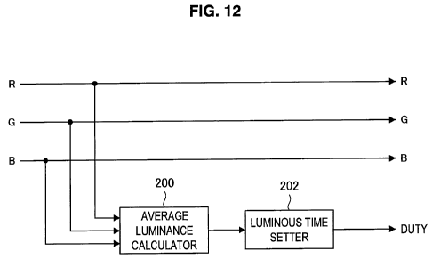
[FIG. 12] FIG. 12 is a block diagram that shows an example of a luminous time
controller
according to an embodiment of the present invention.
[FIG. 13] FIG. 13 is a block diagram that shows an average luminance
calculator
according to an embodiment of the present invention.
[FIG. 14] FIG. 14 is an illustration that shows an example of each V-I ratio
of a
luminescence element for each colour included in a pixel according to an
embodiment of
the present invention.
[FIG. 15] FIG. 15 is an illustration that illustrates the way of deriving a
value held in a
look-up table according to an embodiment of the present invention.
[F1G 16] FIG. 16 is a block diagram that shows an example of the luminous time
controller according to an alternative example of the embodiment of the
present
invention.
[FIG 17] FIG. 17 is the first illustration for illustrating the significance
of a plurality of
average value calculators included in the luminous time controller according
to the
CA 02686436 2009-11-04
11
alternative example of the embodiment of the present invention.
[FIG. 18] FIGz 18 is the second illustration for illustrating the significance
of a plurality of
average value calculators included in the luminous time controller according
to the
alternative example of the embodiment of the present invention.
[FIG. 19] FIG. 19 is an illustration that show an example of the areas for
which the
average luminance is calculated by the average luminance calculator of the
luminous time
controller according to the alternative example of the embodiment of the
present
invention.
[FIG. 20] FIG. 20 is a flow diagram that shows an example of the first method
of
processing a picture signal according to an embodiment of the present
invention.
[FIG. 21] FIG 21 is a flow diagram that shows an example of the second method
of
processing a picture signal according to the embodiment of the present
invention.
Explanation of Reference Numerals
[0044] 100 display device
110 picture signal processor
116 linear converter
126 luminous time controller
132 gamma converter
200, 300 average luminance calculator
202 luminous time setter
250 current ratio adjuster
252 average value calculator
302 first average value calculator
304 second average value calculator
306 average luminance selector
Best Mode for Carrying Out the Invention
[0045] Hereinafter, preferred embodiments of the present invention will be
described in
detail with reference to the appended drawings. Note that, in this
specification and the
drawings, elements that have substantially the same function and structure are
denoted
CA 02686436 2009-11-04
12
with the same reference numerals, and repeated explanation is omitted.
[0046] (Example of Display Device According to Embodiment of Invention)
First, an example of the configuration of a display device according to an
embodiment of the present invention will be described. FIG. 1 is an
illustration that
shows an example of the configuration of the display device 100 according to
an
embodiment of the present invention. Besides, in the following, an organic EL
display,
which is a self-luminescence display device, will be described as an example
of the
display devices according to an embodiment of the present invention. Also, in
the
following, the explanation will be provided with assumption that a picture
signal input
into the display device 100 is a digital signal used in digital broadcasting,
for example,
though it is not limited as such; for example, such a picture signal may be an
analogue
signal used in analogue broadcasting, for example.
[0047] With reference to FIG. 1, the display device 100 includes a controller
104, a
recorder 106, a picture signal processor I 10, a memory 150, a data driver
152, a gamma
circuit 154, an overflowing-current detector 156, and a panel 158.
[0048] The controller 104 includes an MPU (Micro Processing Unit), for
example, and
controls the entire display device 100. The control that is executed by the
controller 104
includes executing a signal process on a signal transmitted from the picture
signal
processor 110, and passing a processing result to the picture signal processor
l 10. Now,
the above signal process by the controller 104 includes, for example,
calculating a gain
for use in adjustment on the luminance of an image to be displayed on the
panel 158, but
is not limited thereto.
[0049] The recorder 106 is one means for storing included in the display
device 100,
and able to hold information for controlling the picture signal processor 110
by the
controller 104. The information held in the recorder 106 includes, for
example, a table
in which parameters are preset for executing by the controller 104 a signal
process on a
signal transmitted from the picture signal processor 110. And, examples of the
recorder
106 include, but are not limited to, magnetic recording media like Hard Disks,
and non
volatile memories like EEPROMs (Electrically Erasable and Programmable Read
Only
Memories), flash memories, MRAMs (Magnetoresistive Random Access Memories),
CA 02686436 2009-11-04
13
FeRAMs (Ferroelectric Random Access Memories), and PRAMs (Phase change Random
Access Memories).
[0050] The signal processor 110 can perform a signal process on a picture
signal input.
In the following, an example of the configuration of the picture signal
processor 110 will
be explained.
[0051 ][One Example of Configuration of Picture Signal Processor 110]
The signal processor 110 includes an edge blurrer 112, an I/F 114, a linear
converter 116, a pattern generator 118, a colour temperature adjuster 120, a
still image
detector 122, a long-term colour temperature adjuster 124, a luminous time
controller 126,
a signal level adjuster 128, an unevenness adjuster 130, a gamma converter
132, a dither
processor 134, a signal output 136, a long-term colour temperature adjusting
detector 138,
a gate pulse output 140, and a gamma circuit controller 142.
[0052] The edge blurrer 112 executes on an input picture signal a signal
process for
blurring the edge. Specifically, the edge blurrer 112 prevents a sticking
phenomenon of
an image onto the panel 158 (which will be described later) by intentionally
shifting an
image that is indicated by the picture signal and blurring its edge. Now, the
sticking
phenomenon is a deterioration phenomenon of luminescence characteristics that
occurs in
the case where the frequency for a particular pixel of the panel 158 to become
luminous
is higher than those of the other pixels. The luminance of a pixel that has
deteriorated of
the sticking phenomenon of an image is lower than the luminance of the other
pixels that
have not deteriorated. Therefore, difference in luminance between a pixel
which has
been and the surrounding pixels which have not deteriorated becomes larger.
Due to
such difference in luminance, users of the display device 100 who see pictures
and
images displayed by the display device 100 would find the screen as if letters
are sticking
on it.
[0053] For example, the I/F 114 is an interface for transmitting/receiving a
signal
to/from elements outside the picture signal processor 110, such as the
controller 104.
[0054] The linear converter 116 executes gamma adjustment on an input picture
signal
to adjust it to a linear picture signal. For example, if the gamma value of an
input signal
is "2.2," the linear converter 116 adjusts the picture signal so that its
gamma value
CA 02686436 2009-11-04
14
becomes "1Ø"
[0055] The pattern generator 118 generates test patterns for use in image
processes
inside the display device 100. The test patterns for used in image processes
inside the
display device 100 include, for example, a test pattern which is used for
display check on
the panel 158, but are not limited thereto.
[0056] The colour temperature adjuster 120 adjusts the colour temperature of
an image
indicated by a picture signal, and adjusts colours to be displayed on the
panel 158 of the
display device 100. Besides, the display device 100 may include colour
temperature
adjusting means (not shown) by which a user who uses the display device 100
can adjust
colour temperature. By the display device 100 including the colour temperature
adjusting means (not shown), users can adjust the colour temperature of an
image
displayed on the screen. Now, examples of the colour temperature adjusting
means (not
shown) which the can be included in the display device include, but are not
limited to,
buttons, directional keys, a rotary selector, such as a Jog-dial, and any
combinations
thereof.
[0057] The still image detector 122 detects a chronological difference between
input
picture signals. And it determines that the input picture signals indicate a
still image if a
predetermined time difference is not detected. The detection result from the
still image
detector 122 may used for preventing a sticking phenomenon on the panel 158
and
inhibiting deterioration of luminescence elements, for example.
[0058] The long-term colour temperature adjuster 124 adjusts aging-related
changes of
red (designated "R" bellow), green (designated "G" below), and blue
(designated "B"
below) sub-pixels included in each pixel of the panel 158. Now, respective
luminescence elements (organic EL elements) for respective colours included in
a
sub-pixel of a pixel vary in L-T characteristics (luminance-time
characteristics). Hence,
with aging-related deterioration of luminescence elements, the colour balance
will be lost
when an image indicated by a picture signal is displayed on the panel 158.
Therefore,
the long-term colour temperature adjuster 124 compensates a luminescence
element
(organic EL element) for each colour included in a sub-pixel for its aging-
related
deterioration.
CA 02686436 2009-11-04
[0059] The luminous time controller 126 controls the luminous time for each
pixel of
the panel 158. More specifically, the luminous time controller 126 controls
the ratio of
the luminous time of a luminescence element to one frame period (or rather,
the ratio of
luminousness to dead screen for one frame period, which will be called a
"duty" below).
The display device 100 can display the image indicated by a picture signal for
a
predetermined time period by applying a current selectively to the pixels of
the panel
158.
[0060] Also, the luminous time controller 126 may control the luminous time
(duty) so
as to prevent the current from overflowing into each of the pixels (strictly,
the
luminescence elements of each of the pixels) of the panel 158. Now an
overflowing
current to be prevented by the luminous time controller 126 mainly represents
the fact (an
overload) that a larger current amount larger than tolerance of the pixels of
the panel 158
flows the pixels. The detail configuration of the luminous time controller 126
according
to the embodiment of the present invention and control over the luminous time
in respect
to the display device 100 according to the embodiment of the present invention
will be
described later.
[0061] The signal level adjuster 128 determines a risk degree for developing
an image
sticking phenomenon in order to prevent the image sticking phenomenon. And,
the
signal level adjuster 128 adjusts luminance of a picture to be displayed on
the panel 158
by adjusting the signal level of a picture signal in order to prevent an image
sticking
phenomenon when the risk degree is equal to or over a predetermined value.
[0062] The long-term colour temperature adjusting detector 138 detects
information for
use by the long-term colour temperature adjuster 124 in compensating a
luminescence
element with its aging-related deterioration. The information detected by the
long-term
colour temperature adjusting detector 138 may be sent to the controller 104
through the
I/F 114 to be recorded onto the recorder 106 via the controller 104.
[0063] The unevenness adjuster 130 adjusts the unevenness, such as horizontal
stripes,
vertical stripes, and spots in the whole screen, which might occur when an
image or a
picture indicated by a picture signal is displayed on the panel 158. For
example, the
unevenness adjuster 130 may perform an adjustment with reference to the level
of an
CA 02686436 2009-11-04
16
input signal and a coordinate position.
[0064] The gamma converter 132 executes a gamma adjustment on the picture
signal
into which a picture signal has been converted to have a linear characteristic
by the linear
converter 116 (more strictly, a picture signal output from the unevenness
adjuster 130) so
as to perform adjustment so that the picture signal have a predetermined gamma
value.
Now, such a predetermined gamma value is a value by which the V-I
characteristic of a
pixel circuit (to be described later) included in the panel 158 of the display
device 100
(voltage-current characteristics; more strictly, the V-I characteristic of a
transistor
included in the picture circuit) can be cancelled. By the gamma converter 132
executing
the gamma adjustment on a picture signal to give it a predetermined gamma
value as
described above, the relation between light amount of an object indicated by
the picture
signal and a current to be applied to luminescence elements can be handled
linearly.
[0065] The dither processor 134 performs a dithering process on the picture
signal
which has been executed a gamma adjustment by the gamma converter 132. Now,
the
dithering is to display with displayable colours combined in order to
represent medium
colours in an environment where the number of available colours is small.
Colours
which can not be normally displayed on the panel can be seemingly represented,
produced by performing dithering by the dither processor 134.
[0066] The signal output 136 outputs to the outside of the picture signal
processor 110
the picture signal on which a dithering process is performed by the dither
processor 134.
Now, the picture signal output from the signal output 136 may be provided as a
signal
separately given for each colour of R, Q and B.
[0067] The gate pulse output 140 outputs a selection signal for controlling
the
luminousness and the luminous time of each pixel of the panel 158. Now, the
selection
signal is based on a duty output by the luminous time controller 126; thus,
for example,
luminescence elements of a pixel may be luminous when a selection signal is at
a high
level, and luminescence elements of a pixel may be not luminous when a
selection signal
is at a low level.
[0068] The gamma circuit controller 142 outputs a predetermined setting value
to the
gamma circuit 154 (to be described later). Now, such a predetermined setting
value
CA 02686436 2009-11-04
17
output from the gamma circuit controller 142 by the gamma circuit controller
142 can be
a reference voltage to be given to a ladder resistance of a D/A converter
(Digital-Analogue Converter) included in the data driver 152 (to be described
later).
[0069] The picture signal processor 110 may execute various signal processes
on an
input picture signal by the configurations described above.
[0070] The memory 150 is alternative means for storing included in the display
device
100. The information held in the memory 150 includes, for example, information
necessary in the case where the signal level adjuster 128 adjusts luminance;
the
information has information on a pixel or a group of pixels which are luminous
at the
luminance over a predetermined luminance and corresponding information on the
exceeding quantity. And, examples of the memory 150 include, but are not
limited to,
volatile memories, such as SDRAMs (Synchronous Dynamic Random Access Memory)
and SRAMs (Static Random Access Memory). For example, the memory 150 may be a
magnetic recording medium, such as a hard disk, or a non volatile memory, such
as a
flash memory.
[0071 ] When an overflowing current is generated due to, for example, a short
circuit on
a substrate (not shown), the overflowing current detector 156 detects the
overflowing
current, and informs the gate pulse output 140 of the generation of the
overflowing
current. For example, the gate pulse output 140 informed of the overflowing
current
generation by the overflowing current detector 156 may refrain from applying a
selection
signal to each pixel of the panel 158, so that the overflowing current is
prevented from
being applied to the panel 158.
[0072] The data driver 152 converts the signal output from the signal output
136 into a
voltage signal to be applied to each pixel of the panel 158, and outputs the
voltage signal
to the panel 158. Now, the data driver 152 may include a D/A converter for
converting
a picture signal as a digital signal into a voltage signal as an analogue
signal.
[0073] The gamma circuit 154 outputs a reference voltage to be given to a
ladder
resistance of the D/A converter included in the data driver 152. The reference
voltage
output to the data driver 152 by the gamma circuit 154 may be controlled by
the gamma
circuit controller 142.
CA 02686436 2009-11-04
18
[0074] The panel 158 is a display included in the display device 100. The
panel 158
has a plurality of pixels arranged in a matrix pattern. Also, the panel 158
has data lines,
to which a voltage signal depending on a picture signal in correspondence to
each pixel is
applied, and scan lines, to which a selection signal is applied. For example,
the panel
158 which displays a picture at definition of SD (Standard Definition) has at
least 640 x
480 = 307200 (Data Lines x Scan Lines) pixels, and if these pixels are formed
out of R, G,
and B sub-pixels for provide coloured display, then it has 640 x 480 x 3 =
921600 (Data
Lines x Scan Lines x Number of Sub-Pixels) sub-pixels. Similarly, the panel
158 which
displays a picture at definition of HD (High Definition) has 1920 x 1080
pixels, and for
coloured display, it has 1920 x 1080 x 3 sub-pixels.
[0075] [Application Example of Sub-pixels: with Organic EL Elements Included]
If the luminescence elements included in a sub-pixel of each pixel are organic
EL elements, the I-L characteristics will be linear. As described above, the
display
device 100 can get the relation between the light amount of an object
indicated by a
picture signal and the current amount to be applied to the luminescence
elements to be
linear by the gamma adjustment by the gamma converter 132. Thus, the display
device
100 can get the relation between the light amount of an object indicated by a
picture
signal and a luminescence amount to be linear, so that a picture and an image
can be
displayed accurately in accordance to the picture signal.
[0076] Also, the panel 158 includes in each pixel a pixel circuit for
controlling a current
amount to be applied. A pixel circuit includes a switching element and a
driving
element for controlling a current amount by an applied scan signal and an
applied voltage
signal, and also a capacitor for holding a voltage signal, for example. The
switching
element and the driving element are formed out of TFTs (Thin Film
Transistors), for
example. Now, because the transistors included in pixel circuits are different
from each
other in V-I characteristic, the V-I characteristic of the panel 158 as a
whole is different
from the V-I characteristics of the panels included in the other display
devices that are
configured similarly to the display device 100. Therefore, the display device
100 gets
the relation between the light amount of an object indicated by a picture
signal and the
current amount to be applied to luminescence elements to be linear by
performing a
CA 02686436 2009-11-04
19
gamma adjustment in correspondence to the panel 158 by the above-described
gamma
converter 132 so as to cancel the V-1 characteristic of the panel 158.
Besides, there will
be described later examples of the configuration of a pixel circuit included
in the panel
158 according to an embodiment of the present invention.
[0077] The display device 100 according to an embodiment of the present
invention can
display a picture and an image according to an input picture signal,
configured as shown
in FIG. 1. Besides, although the picture signal processor 110 is shown in FIG.
1 with the
linear converter 116 followed by the pattern generator 118, it is not limited
to such a
configuration, and a picture signal processor may have the pattern generator
118 followed
by the linear converter 116.
[0078] (Outline of Changes in Signal Characteristics for Display Device 100)
Next, there will be described the outline of changes in signal characteristics
in
respect to the above-described display device 100 according to an embodiment
of the
present invention will be described. Each of FIG. 2A-FIG. 2F is an
illustration that
schematically shows changes in signal characteristics in respect to the
display device 100
according to an embodiment of the present invention.
[0079] Now, each graph in FIG 2A-FIG. 2F shows chronologically a process in
the
display device 100, and the left diagrams in FIG. 2B-FIG. 2E show signal
characteristics
as results of the respective preceding processes; for example, "the signal
characteristic as
a result of the process in FIG. 2A corresponds to the left diagram in FIG.
2B." The right
diagrams in FIG. 2A-FIG. 2E show signal characteristics for use as
coefficients in the
processes.
[0080] [First Signal Characteristic Change: Change due to Process by Linear
Converter
116]
As shown in the left diagram of FIG. 2A, for example, a picture signal
transmitted from a broadcasting station or the like (a picture signal input
into the picture
signal processor 110) has a predetermined gamma value (e.g., "2.2"). The
linear
converter 116 of the picture signal processor 110 adjusts it into a picture
signal with a
characteristic that gives a linear relation between the light amount of an
object indicated
by a picture signal and an output B, by multiplying the gamma curve (linear
gamma: the
CA 02686436 2009-11-04
right diagram of FIG. 2A) that is inverse to the gamma curve (the left diagram
of the FIG.
2A) indicated by the picture signal input into the picture signal processor
110, so that the
gamma value of the picture signal input into the picture signal processor 110
is cancelled.
[0081] [Second Signal Characteristic Change: Change due to Process by Gamma
Converter 132]
The gamma converter 132 of the picture signal processor 110 multiplies the
gamma curve (panel gamma: the right diagram of the FIG. 2B) inverse to the
gamma
curve unique to the panel 158 in advance in order to cancel the V-I
characteristic (the
right diagram of the FIG. 2D) of a transistor included in the panel 158.
[0082] [Third Signal Characteristic Change: Change due to D/A Conversion by
Data
Driver 152]
FIG. 2C shows the case where the picture signal is D/A-converted by the data
driver 152. As shown in FIG. 2C, the picture signal is D/A-converted by the
data driver
152, so that the relation for the picture signal between the light amount of
an object
indicated by the picture signal and the voltage signal into which the picture
signal is
D/A-converted will be as the left diagram of the FIG. 2D.
[0083] [Forth Signal Characteristic Change: Change at Pixel Circuit of Panel
158]
FIG. 2D shows the case where the voltage signal is applied to a pixel circuit
included in the panel 158 by the data driver 152. As shown in FIG. 2B, the
gamma
converter 132 of the picture signal processor 110 has multiplied a panel gamma
in
correspondence to the V-I characteristic of a transistor included in the panel
158 in
advance. Therefore, if the voltage signal is applied to the pixel circuit
included in the
panel 158, the relation for the picture signal between the light amount of an
object
indicated by the picture signal and the current to be applied to the pixel
circuit will be
linear as shown in the left diagram of FIG. 2E.
[0084] [Fifth Signal Characteristic Change: Change at Luminescence element
(Organic
EL Element) of Panel 158]
As shown in the right diagram of FIG. 2E, the I-L characteristic of an organic
EL
element (OLED). Therefore, at a luminescence element of the panel 158, since
both of
the multiplied factors have linear signal characteristics as shown in FIG. 2E,
the relation
CA 02686436 2009-11-04
21
for the picture signal between the light amount of an object indicated by the
picture signal
and the luminescence amount of the luminescence element is a linear relation
(FIG. 2F).
[0085] As shown in FIG. 2A-FIG. 2F, the display device 100 may have a linear
relation
between the light amount of an object indicated by an input picture signal and
the
luminescence amount of a luminescence element. Therefore, the display device
100 can
display a picture and an image accurately according to the picture signal.
[0086] (Example of Configuration of Pixel Circuit Included in Panel 158 of
Display
Device 100)
Next, there will be described an example of the configuration of a pixel
circuit
included in the panel 158 of the display device 100 according to an embodiment
of the
present invention. And, in the following, the explanation will be provided
with
assumption that the luminescence element is an organic EL element, for
example.
[0087] [1] Structure of Pixel Circuit
First, the structure of a pixel circuit included in the panel 158 will be
described.
FIG. 3 is a cross-sectional diagram that shows an example of the cross-
sectional structure
of a pixel circuit provided for the panel 158 of the display device 100
according to the
present invention.
[0088] With reference to FIG. 3, the pixel circuit provided for the panel 158
is
configured to have a dielectric film 1202, a dielectric planarising film 1203,
and a
window dielectric film 1204, each of which is formed in this order on a glass
substrate
1201 where a driving transistor 1022 and the like are formed, and to have
organic EL
elements 1021 provided for recessed parts 1204A in this window dielectric film
1204.
Besides, in FIG. 3, only the driving transistor 1022 of each element of the
driving circuit
is depicted, and depictions for the other elements are omitted.
[0089] An organic EL element 1021 includes an anode electrode 1205 made of
metals
and the like formed at the bottom part of a recessed part 1204A in the above-
mentioned
window dielectric film 1204, and an organic layer (electron transport layer,
luminescence
layer, and hole transmit layer/hole inject layer) 1206 formed on this anode
electrode 1205,
a cathode electrode 1207 made of a transparent conductive film and the like
formed on
this organic layer commonly for all of the elements.
CA 02686436 2009-11-04
22
[0090] In the organic EL element 1021, the organic layer is formed by
sequentially
depositing a hole transmit layer/hole inject layer 2061, and a luminescence
layer 2062, an
electrode transport layer 2063, and an electrode inject layer (not shown) on
the anode
electrode 1205. Now, with a current flowing from the driving transistor 1022
to the
organic layer 1206 through the anode electrode 1205, the organic EL element
1021
becomes luminous when an electron and a hole recombine at the luminescence
layer
2062.
[0091] The driving transistor 1022 includes a gate electrode 1221, a
source/drain area
1223 provided on one side of a semiconductor layer 1222, a drain/source area
1224
provided on the other side of the semiconductor layer 1222, a channel forming
area 1225
which is a part opposite to the gate electrode 1221 of the semiconductor layer
1222.
And, the source/drain area 1223 is electrically connected to the anode
electrode 1205 of
the organic EL element 1021 via a contact hole.
[0092] After the organic EL element 1021 has been formed on a pixel basis on
the glass
substrate 1201 on which the driving circuit is formed, a sealing substrate
1209 is bonded
via a passivation film 1208 by adhesive 1210, and then the organic EL element
1021 is
sealed by this sealing substrate 1209, thus the panel 158 is formed.
[0093] [2] Driving Circuit
Next, an example of the configuration of a driving circuit provided for the
panel
158 will be described.
[0094] The driving circuit included in a pixel circuit of the panel 158
including organic
EL elements could vary depending on the number of transistors and the number
of
capacitors, where the transistors and the capacitors are included in the
driving circuit.
Examples of the driving circuit includes a driving circuit including 5
transistors/I
capacitor (which may be designated below as a"5Tr/1C driving circuit"), a
driving
circuit including 4 transistors/1 capacitor (which may be designated below as
a"4Tr/1C
driving circuit"), a driving circuit including 3 transistors/I capacitor
(which may be
designated below as a"3Tr/1C driving circuit"), and a driving circuit
including 2
transistors/I capacitor (which may be designated below as a"2Tr/1C driving
circuit").
Then, first of all, the common matters amongst the above driving circuits will
be
CA 02686436 2009-11-04
23
described.
[0095] In the following, for reasons of simplicity, each transistor included
in a driving
circuit will be described with the assumption that it includes an n-channel
type TFT.
Besides, a driving circuit according to an embodiment of the present invention
can, of
course, include p-channel type TFTs. And, a driving circuit according to an
embodiment of the present invention can be configured to have transistors
formed on a
semiconductor substrate or the like. In other words, the structure of a
transistor included
in a driving circuit according to an embodiment of the present invention is
not
particularly limited. And, in the following, a transistor included in a
driving circuit
according to an embodiment of the present invention will be described with the
assumption that it is enhancement type, though it is not limited thereto; a
depression type
transistor may be also used. Furthermore, a transistor included in a driving
circuit
according to an embodiment of the present invention may be single gate type or
dual gate
type.
[0096] And, in the following explanation, it is assumed that the panel 158
includes
(N/3) x M pixels arranged in a 2-dimension matrix pattern (M is a natural
number larger
than 1; N/3 is a natural number larger than 1), and that each pixel include
three sub-pixels
(an R luminescence sub-pixel that generates red light, a G luminescence sub-
pixel that
generates green light, and a B luminescence sub-pixel that emits blue light).
And,
luminescence elements included in each pixel are assumed to be line
sequentially driven,
and the display frame rate is represented by FR (frames/sec.). Now,
luminescence
elements included in each of (N/3) pixels arranged in the m-th row (m = 1, 2,
3, ..., M),
or more specifically N sub-pixels, will be driven simultaneously. In other
words, the
timing for emitting light or not of each luminescence element included in one
row is
controlled on the basis of the row to which they belong. Now, the process for
writing a
picture signal onto each pixel included in one row may be a process of writing
a picture
signal simultaneously onto all of the pixels (which may be designated as the
"simultaneous writing process"), or a process of writing a picture signal
sequentially onto
each pixel (which may be designated as the "sequential writing process").
Either of the
writing processes is optionally chosen depending on the configuration of a
driving circuit.
CA 02686436 2009-11-04
24
[0097] And, in the following, driving and operating related to the
luminescence element
located on the m-th row and the n-th column (n = 1, 2, 3, ..., N) will be
described, where
such a luminescence element is designated as the (n, m) luminescence element
or the (n,
m) sub-pixel.
[0098] Until a horizontal scanning period (m-th horizontal scanning period)
for each
luminescence element arranged in m-th row expires, various processes (the
threshold
voltage cancelling process, the writing process, and the mobility adjusting
process, each
of which will be described below) are performed in the driving circuit. Now,
the writing
process and the mobility adjusting process are necessarily performed during
the m-th
horizontal scanning period, for example. And, with some types of driving
circuit, the
threshold voltage cancelling process and the corresponding pre-process can be
performed
prior to the m-th horizontal scanning period.
[0099] Then, after all of the above-mentioned various processes are done, a
luminescence part included in each luminescence element arranged in the m-th
row is
made luminous by the driving circuit. Now, the driving circuit may make the
luminescence parts luminous immediately when all of the above-mentioned
various
processes are done, or after a predetermined period (e.g., a horizontal
scanning period for
the predetermined number of rows) expires. And, such periods can be optionally
set,
depending on the specification of a display device and the configuration of a
driving
circuit and the like. Besides, in the following explanation, for reasons of
simplicity,
luminescence parts are assumed to be made luminous immediately when various
processes are done.
[0100] The luminosity of a luminescence part included in each luminescence
element
arranged in the m-th row is maintained, for example, until just before
beginning of the
horizontal scanning period of each luminescence element arranged in (m + m')-
th row,
where " m' " is determined according to the design specification of a display
device. In
other words, the luminosity of a luminescence part included in each
luminescence
element arranged in the m-th row in a given display frame is maintained until
the (m + m'
- 1)-th horizontal scanning period. And, for example, from the beginning of
the (m +
m')-th horizontal scanning period until the writing process or the mobility
adjusting
CA 02686436 2009-11-04
process are done within the m-th horizontal scanning period in the next
display frame, a
luminescence part included in each luminescence element arranged in the m-th
row
maintains non luminous state. And, the time length of a horizontal scanning
period is a
time length shorter than (I/FR) X(1/M) seconds, for example. Now, if the value
of (m +
m') is above M, the horizontal scanning period for the extra is managed in the
next
display frame, for example.
[0101] By provide the above-mentioned period of non luminous state (which may
be
simply designated as non luminous period in the following), afterimage blur
involved in
active matrix driving is reduced for the display device 100, and quality of
moving image
can be more excellent. Besides, the luminous state/non luminous state of each
sub-pixel
(more strictly a luminescence element included in a sub-pixel) according to an
embodiment of the present invention is not limited as such.
[0102] And, in the following, for two source/drain areas of one transistor,
the term "one
source/drain area" may be used in the meaning of the source/drain area on the
side
connected to a power source. And, the case where a transistor is in ON state
means a
situation that a channel is formed between source/drain areas. It does not
matter here
whether a current flows from one source/drain area of this transistor to
another. And,
the case where a transistor is in OFF state means a situation that no channel
is formed
between source/drain areas. And, the case where a source/drain area of a given
transistor is connected to source/drain area of another transistor embraces a
mode where
the source/drain area of the given transistor and the source/drain area of the
other
transistor possess the same area. Furthermore, a source/drain area can be
formed not
only from conductive materials, such as polysilicon, amorphous silicon and the
like, but
also from metals, alloys, conductive particles, layered structure thereof, and
a layer made
of organic materials (conductive polymers), for example.
[0103] Furthermore, in the following, timing charts would be shown for
explaining
driving circuits according to an embodiment of the present invention, where
lengths (time
lengths) along the transverse axis indicating respective periods are typical,
and they do
not indicate any rate of time lengths of various periods.
[0104] [2-2] Driving Method of Driving Circuit
CA 02686436 2009-11-04
26
Next, a method of driving a driving circuit according to an embodiment of the
present invention will be described. FIG. 4 is an illustration that shows an
equivalent
circuit for a 5Tr/IC driving circuit according to an embodiment of the present
invention.
Besides, in the following, the method of driving a driving circuit according
to an
embodiment of the present invention will be described with an exemplary 5Tr/1C
driving
circuit with reference to FIG. 4, whilst a similar driving method is basically
used for the
other driving circuits.
[0105] A driving circuit according to an embodiment of the present invention
is driven
by (a) the pre-process, (b) the threshold voltage cancelling process, (c) the
writing
process, and (d) the luminescence process shown below, for example.
[0106] (a) Pre-Process
In the pre-process, a first-node initialising voltage is applied to the first
node
NDI, and a second-node initialising voltage is applied to the second node ND2.
Now, the
first-node initialising voltage and the second-node initialising voltage are
applied, so that
the potential difference between the first node ND, and the second node ND2 is
above the
threshold voltage of the driving transistor TRD and the potential difference
between the
second node ND2 and the cathode electrode included in the luminescence part
ELP is not
above the threshold voltage of the luminescence part ELP.
[0107] (b) Threshold Voltage Cancelling Process
In the threshold voltage cancelling process, the voltage of the second node
ND2
is changed towards a voltage obtained by subtracting the threshold voltage of
the driving
transistor TRD from the voltage of the first node NDI, with the voltage of the
first node
ND, maintained.
[0108] More specifically speaking, in order to change the voltage of the first
node ND1
towards the voltage obtained by subtracting the threshold voltage of the
driving transistor
TRD from the voltage of the first node ND,, a voltage which is above a voltage
obtained
by adding the threshold voltage of the driving transistor TRD to the voltage
of the second
node ND2 in the process of (a) is applied to one source/drain area of the
driving transistor
TRD. Now, in the threshold voltage cancelling process, how close the potential
difference between the first node ND, and the second node ND2 (i.e., the
potential
CA 02686436 2009-11-04
27
difference the gate electrode and the source area of the driving transistor
TRD)
approaches to the threshold voltage of the driving transistor TRD depends
qualitatively on
time for the threshold voltage cancelling process. Therefore, as in a mode
where
enough long time is secured for the threshold voltage cancelling process, the
voltage of
the second node ND2 reaches at the voltage obtained by subtracting the
threshold voltage
of the driving transistor TRD from the voltage of the first node ND], and the
driving
transistor TRD gets in OFF state. On the other hand, as in a mode where there
is no
choice but to set the time for the threshold voltage cancelling process short,
the potential
difference between the first node NDI and the second node ND2 may be larger
than the
threshold voltage of the driving transistor TRD, and the driving transistor
TRD may be
not get in OFF state. Hence, in the threshold voltage cancelling process, the
driving
transistor TRD does not necessarily get in OFF state as a result of the
threshold voltage
cancelling process,
[0109] (c) Writing Process
In the writing process, a picture signal is applied to the first node ND, from
the
data line DTL via the writing transistor TRw that is made to be in ON state by
a signal
from the scan line SCL.
[0110] (d) Luminescence Process
In the Luminescence Process, the luminescence part ELP become luminous (is
driven) by making the writing transistor TRw to be in OFF state by a signal
from the scan
line SCL to make the first node ND, to be in floating state and running a
current
depending on the value of the potential difference between the first node NDi
and the
second node ND2 from the power source unit 2100 to the luminescence part ELP
via the
driving transistor TRp.
[0111 ] A driving circuit according to an embodiment of the present invention
is driven
by the above processes of (a)-(d), for example.
[0112] [2-3] Examples of Configuration of Driving Circuit and Specific
Examples of
Driving Method
Next, for each driving circuit, examples of the configurations of the driving
circuits and a method of driving such driving circuits will be described
specifically below.
CA 02686436 2009-11-04
28
Besides, in the following, a 5Tr/1C driving circuit and a 2Tr/1C driving
circuit out of
various driving circuits will be described.
[0113] [2-3-1] 5Tr/1C Driving Circuit
First, a 5Tr/IC driving circuit will be described with reference to FIG. 4-FIG
61.
FIG. 5 is a timing chart for driving of the 5Tr/IC driving circuit according
to an
embodiment of the present invention. FIG. 6A-FIG. 61 are illustrations that
typically
show respective ON/OFF states of the transistors included in the 5Tr/IC
driving circuit
according to an embodiment of the present invention shown in FIG 4, etc.
[0114] With reference to FIG. 4, the 5Tr/1C driving circuit includes a writing
transistor
TRw, a driving transistor TRD, a first transistor TRI, a second transistor
TR2, a third
transistor TR3, and a capacitor Cl;namely, the 5Tr/1C driving circuit includes
five
transistors and one capacitor. Besides, in the example shown in FIG. 4, the
writing
transistor TRw, the first transistor TRI, the second transistor TR2, and the
third transistor
TR3 are formed out of n-channel type TFTs, though they are not limited
thereto; they may
also be formed out of p-channel type TFTs. And, the capacitor C, may be formed
out of
a capacitor with a predetermined capacitance.
[0115] <First Transistor TR>>
One source/drain area of the first transistor TRI is connected to a power
source
unit 2100 (voltage V,J, and the other source/drain area of the first
transistor TRI is
connected to one source/drain area of the driving transistor TRD. And, the
ON/OFF
operation of the first transistor TRI is controlled by a first-transistor
control line CLI,
which is extended from a first-transistor control circuit 2111 to connect to
the gate
electrode of the first transistor TRI. Now, the power source unit 2100 is
provided for
supply a current to a luminescence part ELP to make the luminescence part ELP
luminous.
[0116] <Driving Transistor TRD>
One source/drain area of the driving transistor TRD is connected to the other
source/drain area of the first transistor TRI. And, the other source/drain
area of the
driving transistor TRD is connected to the anode electrode of the luminescence
part ELP,
the other source/drain area of the second transistor TR2, and one source/drain
area of the
CA 02686436 2009-11-04
29
capacitor Cl, and forms a second node ND2. And, the gate electrode of the
driving
transistor TRD is connected to the other source/drain area of the writing
transistor TRw,
the other source/drain area of the third transistor TR3, and the other
electrode of the
capacitor Cl, and forms a first node NDI.
[0117] Now, in the case of the luminous state of a luminescence element, the
driving
transistor TRD is driven to flow a drain current Ids according to Equation I
below, for
example, where " " shown in Equation 1 denotes a "effective mobility," and "L"
denotes
a "channel length." And similarly, "W" shown in Equation I denotes a "channel
width," "Vgs" denotes the "potential difference between the gate electrode and
the source
area, "Vth" denotes a "threshold voltage," "CoX" denotes "(Relative
Permittivity of Gate
Dielectric Layer) x (Permittivity of Vacuum) / (Thickness of Gate Dielectric
Layer)," and
"k" denotes "k = (1/2) = (W/L) = CoX," respectively.
[0118] Ids = k ' (Vg, - Vtn)z
... Equation 1
[0119] And, in the case of the luminous state of a luminescence element, one
source/drain area of the driving transistor TRD works as a drain area, and the
other
source/drain area works as a source area. Besides, in the following, for the
reason of
simplicity of explanation, in the following explanation, one source/drain area
of the
driving transistor TRD may be simply designated as the "drain area", and the
other
source/drain area may be simply designated as the "source area".
[0120] The luminescence part ELP becomes luminous due to the drain current Ids
shown
in Equation I flowing thereto, for example. Now, the luminescence state
(luminance) of
the luminescence part ELP is controlled depending on the magnitude of the
value of the
drain current Ids.
[0121] <Writing Transistor TRw>
The other source/drain area of the writing transistor TRw is connected to the
gate
electrode of the driving transistor TRD. And, one source/drain area of the
writing
transistor TRD is connected a data line DTL, which is extended from a signal
output
circuit 2102. Then, a picture signal Vsig for controlling the luminance of the
luminescence part ELP is supplied to the one source/drain area via the data
line DTL.
CA 02686436 2009-11-04
Besides, various signals and voltages (signals for pre-charge driving, various
reference
voltages, etc.) except for the picture signal Vsig may be supplied to the one
source/drain
area via the data line DTL. And, the ON/OFF operation of the writing
transistor TRw is
controlled by a scan line SCL, which is extended from a scanning circuit 2101
to connect
to the gate electrode of the writing transistor TRw.
[0122] <Second Transistor TR2>
The other source/drain area of the second transistor TR2 is connected to the
source area of the driving transistor TRD. And, a voltage Vss for initialising
the
potential of the second node ND2 (i.e., the potential of the source area of
the driving
transistor TRD) is supplied to one source/drain area of the second transistor
TR2. And,
the ON/OFF operation of the second transistor TR2 is controlled by a second-
transistor
control line AZ2, which is extended from a second-transistor control circuit
2112 to
connect to the gate electrode of the second transistor TR2.
[0123] <Third Transistor TR3>
The other source/drain area of the third transistor TR3 is connected to the
gate
electrode of the driving transistor TRD. And, a voltage Vofs for initialising
the potential
of the first node ND1 (i.e., the potential of the gate electrode of the
driving transistor
TRD) is supplied to one source/drain area of the third transistor TR3. And,
the ON/OFF
operation of the third transistor TR3 is controlled by a third-transistor
control line AZ3,
which is extended from a third-transistor control circuit 2113 to connect to
the gate
electrode of the third transistor TR3.
[0124] <Luminescence Part ELP>
The anode electrode of the luminescence part ELP is connected to the source
area of the driving transistor TRD. And, a voltage Vcat is applied to the
cathode
electrode of the luminescence part ELP. In FIG. 4, the capacitance of the
luminescence
part ELP is represented by a symbol: CEL. And, a threshold voltage which is
necessary
for the luminescence part ELP to be luminous is represented by Vth_EL. Then,
when
voltage equal to or more than V,h_EL is applied between the anode and cathode
electrodes
of the luminescence part ELP, the luminescence part ELP becomes luminous.
[0125] Besides, in the following, "Vsig" represents a picture signal for
controlling
CA 02686436 2009-11-04
31
luminance of the luminescence part ELP, "Vcc" represents the voltage of the
power
source unit 2100, and "Vof," represents the voltage for initialising the
potential of the
gate electrode of the driving transistor TRD (the potential of the first node
NDI). And,
in the following, "Vss" represents the voltage for initialising the potential
of the source
area of the driving transistor TRD (the potential of the second node ND2),
"Vth" represents
a threshold voltage of the driving transistor TRD, "Vcat" represents the
voltage applied to
the cathode electrode of the luminescence part ELP, and "Vth-EL" represents a
threshold
voltage of the luminescence part ELP. Furthermore, in the following, the
respective
values of voltages or potentials are explained, given as follows for example,
though
respective values of voltages or potentials according to an embodiment of the
present
invention are not limited as follows, of course.
Vsig: 0 [volt] - 10 [volt]
Vcc: 20 [volt]
VOfs: 0 [volt]
Vss: - 10 [volt]
Vth: 3 [volt]
Vcat: 0 [volt]
Vth-EL: 3 [volt]
[0126] In the following, with reference to FIG. 5 and FIG. 6A-FIG 61, the
operation of a
5Tr/1C driving transistor will be described. Besides, in the following, the
explanation
will be provided with the assumption that luminous state starts immediately
after all of
the above-described various processes (the threshold voltage cancelling
process, the
writing process, the mobility adjusting process) are done in the 5Tr/1C
driving transistor,
though it is not limited thereto. The explanations of 4Tr/1C driving circuit,
3Tr/1C
driving circuit, and 2Tr/1C driving circuit are similarly provided below.
[0127] <A-1> [Period -TP(5)-,] (see FIG. 5 and FIG 6A)
[Period -TP(5)-,] indicates, for example, an operation in the previous display
frame, and is a period for which the (n, m) luminescence element is in
luminous state
after the last various processes are done. Thus, a drain current I' based on
the equation
(5) below flows into a luminescence part ELP of a luminescence element
included in the
CA 02686436 2009-11-04
32
(n, m) sub-pixel, and the luminance of the luminescence element included in
the (n, m)
sub-pixel is a value depending on this drain current I'. Here, the writing
transistor TRw,
the second transistor TR2, and the third transistor TR3 are in OFF state, and
the first
transistor TRI and the driving transistor TRD are in ON state. The luminous
state of the
(n, m) luminescence element is maintained until just before the beginning of
the
horizontal scanning period for a luminescence element arranged in the (m + m')-
th row.
[0128] [Period -TP(5)o] - [Period -TP(5)4] are operation periods laid after
the
luminous state after completion of the last various processes ends, and just
before the
next writing process is executed. In other words, these [Period -TP(5)o] -
[Period
-TP(5)4] corresponds to the period of a particular time length from the
beginning of the
(m + m')-th horizontal scanning period in the previous display frame to the
end of the (m
- 1)-th horizontal scanning period in the current display frame. Besides,
[Period
-TP(5)o] - [Period -TP(5)4] may be configured to be included within the m-th
horizontal scanning period in the current display frame.
[0129] And, for [Period -TP(5)o] - [Period -TP(5)4], the (n, m) luminescence
element
is basically in non luminous state. In other words, for [Period -TP(5)o] -
[Period
-TP(5)1] and [Period -TP(5)3] - [Period -TP(5)4], the luminescence element
does not
emit light since the first transistor TRI is in OFF state. Now, for [Period -
TP(5)2], the
first transistor TRI is in ON state. However, the threshold voltage cancelling
process to
be described below is executed for [Period -TP(5)2]. Therefore, given that
Equation 2
below is satisfied, the luminescence element will not be luminous.
[0130] In the following, each period of [Period -TP(5)o] - [Period -TP(5)4]
will be
described. Besides, the beginning of [Period -TP(5)1], and the length of each
period of
[Period -TP(5)o] - [Period -TP(5)4] are optionally set according the settings
of the
display device 100.
[0131] <A-2> [Period -TP(5)o]
As described above, for [Period -TP(5)o], the (n, m) luminescence element is
in
non luminous state. And, the writing transistor TRw, the second transistor
TR2, and the
third transistor TR3 are in OFF state. Now, because the first transistor TRI
gets into
OFF state at the time point for transition from [Period -TP(5)_1] to [Period -
TP(5)o],
CA 02686436 2009-11-04
33
the potential of the second node ND2 (the source area of the driving
transistor TRD or the
anode electrode of the luminescence part ELP) is lowered to (Vth-EL + VCat),
and the
luminescence part ELP gets into non luminous state. And, as the potential of
the second
node ND2 gets lower, the potential of the first node ND, in floating state
(the gate
electrode of the driving transistor TRD) is also lowered.
[0132] <A-3> [Period -TP(5)1] (see FIG. 5, FIG. 6B and FIG. 6C)
For [Period -TP(5)1], there is executed a pre-process for executing the
threshold voltage cancelling process. More specifically, at the beginning of
[Period
-TP(5), ], the second transistor TR2 and the third transistor TR3 are got into
ON state by
getting the second-transistor control line AZ2 and the third-transistor
control line AZ3 to
be at high level. As a result, the potential of the first node ND, becomes
Vofs (e.g., 0
[volt]), and the potential of the second node ND2 becomes Vss (e.g., - 10
[volt]). Then,
before the expiration of [Period -TP(5)1], the second transistor TR2 is got
into OFF state
by getting the second-transistor control line AZ2 to be at low level. Now, the
second
transistor TR2 and the third transistor TR3 may be synchronously got into ON
state,
though they are not limited as such; for example, the second transistor TR2
may be first
got into ON state, or the third transistor TR3 may be first got into ON state.
[0133] By the process above, the potential between the gate electrode and
source area of
the driving transistor TRD becomes above Vth. Now, the driving transistor TRD
is in ON
state.
[0134] <A-4> [Period -TP(5)2] (see FIG. 5 and FIG. 6D)
For [Period -TP(5)2], the threshold voltage cancelling process is executed.
More specifically, the first transistor TRI is got into ON state by getting
the
first-transistor control line CLI to be at high level with the third
transistor TR3 maintained
in ON state. As a result, the potential of the first node ND, does not change
(Vofs = 0
[volt] maintained), whilst the potential of the second node ND2 changes
towards the
potential obtained by subtracting the threshold voltage Vth of the driving
transistor TRD
from the potential of the first node NDI. In other words, the potential of the
second
node ND2 in floating state increases. Then, when the potential difference
between the
gate electrode and source area of the driving transistor TRD reaches to Vth,
the driving
CA 02686436 2009-11-04
34
transistor TRD gets into OFF state. Specifically, the potential of the second
node ND2 in
floating state approaches to (Vofs - Vth= - 3 [volt] > Vss) to be (VOfs - Vth)
in the end.
Now, if Equation 2 below is assured, in other words, if the potentials are
selected and
determined to satisfy Equation 2, the luminescence part ELP will not be
luminous.
[0135] (VOfs - Vth) < (Vth-EL+ VCat)
... Equation 2
[0136] For [Period -TP(5)5], the potential of the second node ND2 will be
(VOfs - Vth)
eventually. Now, the potential of the second node ND2 is determined, depending
on the
threshold voltage Vth of the driving transistor TRD, and on the potential Vofs
for
initialising the gate electrode of the driving transistor TRD; namely the
potential of the
second node ND2 does not depend on the threshold voltage Vth-EL of the
luminescence
part ELP.
[0137] <A-5> [Period -TP(5)3] (see FIG. 5 and FIG. 6E)
For [Period -TP(5)3], the first transistor TRI is got into OFF state by
getting the
first-transistor control line CL, to be at low level with the third transistor
TR3 maintained
in ON state. As a result, the potential of the first node ND, does not change
(Vofs = 0
[volt] maintained), nor the potential of the second node ND2 does not change.
Therefore,
the potential of the second node ND2 is maintained (Vofs - Vth =- 3 [volt]).
[0138] <A-6> [Period -TP(5)4] (see FIG 5 and FIG. 6F)
For [Period -TP(5)4], the third transistor TR3 is got into OFF state by
getting
the third-transistor control line AZ3 to be at low level. Now, the potentials
of the first
node NDl and the second node ND2 do not change substantially. Besides, in
practice,
potential changes might occur by electrostatic bonding of parasitic
capacitances or the
like; however, these can be normally neglected.
[0139] For [Period -TP(5)o] - [Period -TP(5)4], a 5Tr/1C driving transistor
operates
as described above. Next, each period of [Period -TP(5)5] - [Period -TP(5)7]
will be
described. Now, the writing process is executed for [Period -TP(5)5], and the
mobility
adjusting process is executed for [Period -TP(5)6]. The above-mentioned
processes
are necessarily executed within the m-th horizontal scanning period, for
example. In the
following, for the reason of simplicity of the explanation, the explanation
will be
CA 02686436 2009-11-04
provided with the assumption that the beginning of [Period -TP(5)5] and the
end of
[Period -TP(5)6] match the beginning and end of the m-th horizontal scanning
period,
respectively.
[0140] <A-7> [Period -TP(5)5] (see FIG 5 and FIG. 6G)
For [Period -TP(5)5], the writing process for the driving transistor TRD is
executed. Specifically, the data line DTL is made to be Vsig for controlling
the
luminance of the luminescence part ELP with the first transistor TRI, the
second
transistor TR2, and the third transistor TR3 maintained in OFF state; next,
the writing
transistor TRw is got into ON state by getting the scan line SCL to be at high
level. As a
result, the potential of the first node ND, increases to Vsig.
[0141] Now, the value of the capacitance of the capacitor C, is represented by
cl, the
value of the capacitance of the capacitance CEL of the luminescence part ELP
is
represented by CEL, and the value of the parasitic capacitance between the
gate electrode
and source area of the driving transistor TRD is represented by cgs. When the
potential
of the gate electrode of the driving transistor TRD changes from Vofs to Vsig
(>Vofs), the
potentials of both sides of the capacitor C, (the potentials of the first node
NDI and the
second node ND2) basically change. In other words, potentials based on the
change
(Vsig - Vofs) of the potential of the gate electrode of the driving transistor
TRD (= the
potential of the first node NDI) are allotted to the capacitor Cl, the
capacitance CEL of the
luminescence part ELP, and the parasitic capacitance between the gate
electrode and
source area of the driving transistor TRD. Thus, if the value CEL is enough
larger than
the value c, and the value cgs, the change of the potential of the source area
of the driving
transistor TRD (the second node ND2) based on the change (Vsig - Vofs)of the
potential of
the driving transistor TRD is small. Now, in general, the capacitance value
CEL of the
capacitance CEL of the luminescence part ELP is larger than the capacitance
value ci of
the capacitor C, and the value cgs of the parasitic capacitance of the driving
transistor
TRD. Thus, in the following, for the reason of simplicity of the explanation,
the
explanation will be provided, except for the cases in particular necessities,
without any
regard to potential changes of the second node ND2 which occur by potential
changes of
the first node NDI. It is the same as described above for the other driving
circuits
CA 02686436 2009-11-04
36
shown below. And, FIG 5 is shown without any regard to potential changes of
the
second node ND2 which occur by potential changes of the first node NDI.
[0142] And, the value of Vg is as "Vg = Vsig" and the value of VS is as "Vs z
Vofs - Vth,"
where Vg is the potential of the gate electrode of the driving transistor TRD
(the first node
NDI) and VS is the potential of the source area of the driving transistor TRD
(the second
node NDZ). Therefore, the potential difference between the first node NDt and
the
second node ND2, namely the potential difference Vgs between the gate
electrode and
source area of the driving transistor TRD can be expressed by Equation 3
below.
[0143] Vgs -usig - (Vofs - uth)
... Equation 3
[0144] As shown in Equation 3, Vgs obtained in the writing process for the
driving
transistor TRD depends on only the picture signal Vs;g for controlling the
luminance of the
luminescence part ELP, the threshold voltage Vth of the driving transistor
TRD, and the
voltage Vofs for initialising the gate electrode of the driving transistor
TRD. And it can
be seen from Equation 3 that Vgs obtained in the writing process for the
driving transistor
TRD does not depend on the threshold voltage Vth_EL of the luminescence part
ELP.
[0145] <A-8> [Period -TP(5)6] (see FIG 5FIG. 6H)
For [Period -TP(5)6], an adjustment (mobility adjustment process) on the
potential of the source area of the driving transistor TRD (the second node
ND2) based on
the magnitude of the mobility of the driving transistor TRD is executed.
[0146] In general, if the driving transistor TRD is made of a polysilicon film
transistor or
the like, it is hard to avoid that the mobility varies amongst transistors.
Therefore,
even if picture signals Vsigs of the same value are applied to gate electrodes
of a plurality
of driving transistors TRDS of different mobility s, there might be found a
difference
between a drain current Ids flowing a driving transistor TRD with large
mobility and a
drain Ids flowing a driving transistor TRD with small mobility . Then, if
such a
difference occurs, the uniformity of the screen of the display device 100 will
be lost.
[0147] Then, for [Period -TP(5)6], the mobility adjusting process is executed
in order
to prevent the issues described above from occurring. Specifically, the first
transistor
TRI is got into ON state by getting the first transistor control line CL, to
be at high level
CA 02686436 2009-11-04
37
with the writing transistor TRw maintained in ON state; next, by getting the
first
transistor control line CL1 to be at high level after a predetermined time
(to) has passed,
the first transistor TRI is got into ON state, and next, by getting the scan
line SCL to be at
low level after a predetermined time (to) has passed, the writing transistor
TRw is got into
OFF state, and the first node NDi (the gate electrode of the driving
transistor TRD) is got
into floating state. As a result, if the value of the mobility g of the
driving transistor
TRD is large, then the increased amount AV (potential adjustment value) of the
potential
of the source area of the driving transistor TRD is large, and if the value of
the mobility g
of the driving transistor TRD is small, then the increased amount AV
(potential adjustment
value) of the potential of the source area of the driving transistor TRD is
small. Now, the
potential difference Vgs between the gate electrode and source area of the
driving
transistor TRD is transformed, for example, as Equation 4 below, based on
Equation 3.
[0148] Vgs ;:tVsig - (Vofs - Vth) - OV
... Equation 4
[0149] Besides, the predetermined time for executing the mobility adjusting
process
(the total time to of [Period -TP(5)6]) can be determined in advance as a
configuration
value during the configuration of the display device 100. And, the total time
to of
[Period -TP(5)6] can be determined so that the potential of the source area of
the driving
transistor TRD in this case (Vofs - Vth + AV) satisfy Equation 5 below. In
such a case,
the luminescence part ELP will not be luminous for [Period -TP(5)6]. Moreover,
an
adjustment on the variation of the coefficient k(=(1/2) =(W/L) = Co,t) is also
executed simultaneously by this mobility adjusting process.
[0150] VOfs - Vth + AV `_- (Vth-EL + VCat)
... Equation 5
[0151] <A-9> [Period -TP(5)7] (see FICx 61)
By the above-described operations, the threshold voltage cancelling process,
the
writing process, and the mobility adjusting process are done. Now, for [Period
-TP(5)7], low level of the scan line SCL results in OFF state of the writing
transistor
TRw and floating state of the first node NDI, namely the gate electrode of the
driving
transistor TRD. On the other hand, the first transistor TRI maintains ON
state, the drain
CA 02686436 2009-11-04
38
area of the driving transistor TRD is in connection with the power source 2100
(voltage
V,,, e.g., 20 [volt]). Thus, for [Period -TP(5)7], the potential of the second
transistor
TR2 increases.
[0152] Now, the gate electrode of the driving transistor TRD is in floating
state, and
because of the existence of the capacitor C1, the same phenomenon as in so-
called
bootstrap circuit occurs in the gate electrode of the driving transistor TRD,
and also the
potential of the first node ND, increases. As a result, the potential
difference Vgs
between the gate electrode and source area of the driving transistor TRD
maintains the
value of Equation 4.
[0153] And, for [Period -TP(5)7], the luminescence part ELP starts to be
luminous
because the potential of the second node ND2 increases to be above (Vth_EL +
Vcat). At
this point, the current flowing to the luminescence part ELP can be expressed
by
Equation labove because it is the drain current Ids flowing from the drain
area of the
driving transistor TRD to the source area of the driving transistor TRD;
where, from
Equation I above and Equation 4 above, Equation 1 above can be transformed
into
Equation 6 below.
[0154] Ids - k ' g . (VSig - Vofs - AV)2
... Equation 6
[0155] Therefore, for example, if Vofs is set to 0 [volt], the current Ids
flowing to the
luminescence part ELP is proportional to the square of the value obtained by
subtracting
the value of the picture signal Vsig for controlling the luminance of the
luminescence part
ELP from the value of the potential adjustment value AV of the second node ND2
(the
source area of the driving transistor TRD) resulted from the mobility g of the
driving
transistor TRD. In other words, the current Ids flowing to the luminescence
part ELP
does not depend on the threshold voltage Vtn_EL of the luminescence part ELP
and the
threshold voltage Vth of the driving transistor TRD; namely, the luminescence
amount
(luminance) of the luminescence part ELP is not affected by the threshold
voltage Vth_EL
of the luminescence part ELP and the threshold voltage Vth of the driving
transistor TRD.
Then, the luminance of the (n, m) luminescence element is a value
corresponding to this
current Ids.
CA 02686436 2009-11-04
39
[0156] And, larger mobility of the driving transistor TRD results in a
larger potential
adjustment value AV, then the value of Vgs on the left side of Equation 4
above becomes
smaller. Therefore, even if the value of the mobility is large in Equation
6, the value
of (Vs;g - VofS - AV)2 becomes small, and as a result, the drain current Ids
can be adjusted.
Thus, also if values of picture signal Vs;gs are the same amongst driving
transistors TRDs
with different mobility , the drain currents Idss will be almost the same,
and as a result,
the currents Idss flowing to the luminescence part ELP for controlling the
luminance of
the luminescence part ELP is uniformed. Thus, a 5Tr/1C driving circuit can
adjust the
variation of the luminance of the luminescence parts resulted from the
variation of the
mobility (and further, the variation of k).
[0157] And, luminous state of the luminescence part ELP is maintained until
the (m +
m' - 1)-th horizontal scanning period. This time point corresponds to the end
of [Period
-TP(5)_t].
[0158] A 5Tr/IC driving circuit makes a luminescence element luminous by
operating
as described above.
[0159] [2-3-2] 2Tr/1C Driving Circuit
Next, a 2Tr/1C driving circuit will be described. FIG. 7 is an illustration
that
shows an equivalent circuit for the 2Tr/1C driving circuit according to an
embodiment of
the present invention. FIG 8 is a timing chart for driving of the 2Tr/1C
driving circuit
according to an embodiment of the present invention. FIG 9A-FIG. 9F are
illustrations
that typically show ON/OFF state of each of the transistors included in the
2Tr/IC
driving circuit according to an embodiment of the present invention, etc.
[0160] With reference to FIG. 7, the 2Tr/1C driving circuit omits three
transistors, which
are the first transistor TRi, the second transistor TR2, and the third
transistor TR3, are
omitted from the 5Tr/IC driving circuit shown in FIG. 4 described above. In
other
words, the 2Tr/lC driving circuit includes a writing transistor TRw, a driving
transistor
TRw, and a capacitor C1.
[0161] <Driving Transistor TRE)>
The detailed explanation of the configuration the driving transistor TRD is
omitted since it is the same as the configuration of the driving transistor
TRD described
CA 02686436 2009-11-04
with regard to the 5Tr/1C driving circuit shown in FIG 4. Besides, the drain
area of the
driving transistor TRD is connected to the power source unit 2100. And, from
the power
source unit 2100, the voltage VCC-x for getting the luminescence part ELP
luminous and
the voltage VCC-L for controlling the potential of the source area of the
driving transistor
TRD are supplied. Now, the values of the voltages VCC-H and VCC-L could be as
"VCC-x =
20 [volt]" and "VCC-L 10 [volt]," for example, though they are not limited
thereto, of
course.
[0162] <Writing Transistor TRW>
The configuration of the writing transistor TRw is the same as the
configuration
of the writing transistor TRw described with regard to the 5Tr/1 C driving
circuit shown in
FIG. 4. Therefore, the detailed explanation of the configuration the writing
transistor
TRw is omitted.
[0163] <Luminescence Part ELP>
The configuration of the luminescence part ELP is the same as the
configuration
of the luminescence part ELP described with regard to the 5Tr/IC driving
circuit shown
in FIG. 4. Therefore, the detailed explanation of the configuration the
luminescence part
ELP is omitted.
[0164] In the following, the operation of the 2Tr/1C driving circuit will be
described
with reference to FIG. 8 and FIG 9A-FIG. 9F, respectively.
[0165] <B-I> [Period -TP(2)-,] (see FIG. 8 and FIG. 9A)
[Period -TP(2)-,] indicates, for example, an operation for a previous display
frame, and it is substantially the same operation as that of [Period -TP(5)-,]
shown in
FIG. 5 described with regard to the 5Tr/1C driving circuit.
[0166] [Period -TP(2)o] -[Period -TP(2)2] shown in FIG. 8 are periods
corresponding
to [Period -TP(5)o] - [Period -TP(5)4] shown in FIG. 5, and operation periods
until just
before the next writing process is executed. And, for [Period -TP(2)o] -
[Period
-TP(2)21, similarly to the 5Tr/1C driving circuit described above, the (n, m)
luminescence element is basically in non luminous state. Now, the operation of
the
2Tr/1C driving circuit is different from the operation of the 5Tr/1C driving
circuit in that
[Period -TP(2)1] - [Period -TP(2)2] are included in the m-th horizontal
scanning period
CA 02686436 2009-11-04
41
in addition to [Period -TP(2)3] , as shown in FIG. 8. Besides, in the
following, for the
reason of simplicity of the explanation, the explanation will be provided with
the
assumption that the beginning of [Period -TP(2)1] and the end of [Period -
TP(2)3]
match the beginning and end of the m-th horizontal scanning period,
respectively.
[0167] In the following, each period of [Period -TP(2)0] - [Period -TP(2)2]
will be
described. Besides, the length of each period of [Period -TP(2)1] - [Period -
TP(2)2]
can be optionally set according to the settings of the display device 100,
similarly to the
5Tr/1C driving circuit described above.
[0168] <B-2> [Period -TP(2)o] (see FIG. 8 and FIG. 9B)
[Period -TP(2)o] indicates, for example, an operation from the previous
display
frame to the current display frame. More specifically, [Period -TP(2)o] is a
period
from the (m + m')-th horizontal scanning period in the previous display frame
to the (m -
1)-th horizontal scanning period in the current display frame. And for this
[Period
-TP(2)o], the (n, m) luminescence element is in non luminous state. Now, at
the time
point for transition from [Period -TP(2)-,] to [Period -TP(2)o], the voltage
supplied
from the power source unit 2100 is switched from VCC-x to voltage VCC-L. As a
result,
the potential of the second node ND2 is lowered to VcC-L, and the luminescence
part ELP
gets into non luminous state. And, as the potential of the second node ND2
gets lower,
the potential of the first node ND, in floating state (the gate electrode of
the driving
transistor TRD) is also lowered.
[0169] <B-3> [Period -TP(2)1] (see FIG. 8 and FICL 9C)
The horizontal scanning period for the m-th row begins at [Period -TP(2)1].
Now, for this [Period -TP(2)1], a pre-process for executing the threshold
voltage
cancelling process is executed. At the beginning of [Period -TP(2)1], the
writing
transistor TRw is got into ON state, by getting the potential of the scan line
SCL to be at
high level. As a result, the potential of the first node ND1 becomes Vofs
(e.g., 0 [volt]).
And, the potential of the second node ND2 is maintained at VCC_L (e.g., - 10
[volt]).
[0170] Thus, for [Period -TP(2)1], the potential between the gate electrode
and source
area of the driving transistor TRD becomes above Vth, and the driving
transistor TRD gets
into ON state.
CA 02686436 2009-11-04
42
[0171 ]<B-4> [Period -TP(2)2] (see FIG. 8 and FIG. 9D)
The threshold voltage cancelling process is executed for [Period -TP(2)2].
Specifically, for [Period -TP(2)2], the voltage supplied from the power source
unit 2100
is switched from VCC_L to the voltage VCC_H, with the writing transistor TRW
maintained
in ON state. As a result, for [Period -TP(2)2], the potential of the first
node ND, does
not change (Voes = 0 [volt] maintained), whilst the potential of the second
node ND2
changes towards the potential obtained by subtracting the threshold voltage
Vth of the
driving transistor TRD from the potential of the first node NDI. Hence, the
potential of
the second node ND2 in floating state increases. Then, when the potential
difference
between the gate electrode and source area of the driving transistor TRD
reaches to Vth,
the driving transistor TRD gets into OFF state. More specifically, the
potential of the
second node ND2 in floating state approaches to (VoeS - Vth= - 3 [volt]) to be
(Vofs - Vth)
in the end. Now, if Equation 2 above is assured, in other words, if the
potentials are
selected and determined to satisfy Equation 2 above, the luminescence part ELP
will not
be luminous.
[0172] For [Period -TP(2)3], the potential of the second node ND2 will be
(Vofs - Vth)
eventually. Therefore, the potential of the second node ND2 is determined,
depending
on the threshold voltage Vth of the driving transistor TRD, and on the
potential Vofs for
initialising the gate electrode of the driving transistor TRD. In other words,
the potential
of the second node ND2 does not depend on the threshold voltage Vth_EL of the
luminescence part ELP.
[0173] <B-5> [Period -TP(2)3] (see FIG. 8 and FIG. 9E)
For [Period -TP(2)3], the writing process for the driving transistor TRD, and
an
adjustment (mobility adjustment process) on the potential of the source area
of the
driving transistor TRD (the second node ND2) based on the magnitude of the
mobility
of the driving transistor TRD are executed. Specifically, for [Period -
TP(2)3], the data
line DTL is made to be Vs;g for controlling the luminance of the luminescence
part ELP
with the writing transistor TRw maintained in OFF state. As a result, the
potential of the
first node ND, increases to Vsig, and the driving transistor TRD gets into ON
state.
Besides, the way of bringing the driving transistor TRD into ON state is not
limited
CA 02686436 2009-11-04
43
thereto; for example, the driving transistor TRD gets into ON state by
bringing the writing
transistor TRw into ON state. Hence, for example, the 2Tr/1C driving circuit
can bring
the driving transistor TRD into ON state by getting the writing transistor TRw
into OFF
state temporally, changing the potential of the data line DTL into a picture
signal Vsig for
controlling the luminance of the luminescence part ELP, getting the scan line
SCL to be
at high level, and then bringing the writing transistor TRw into ON state.
[0174] Now, for [Period -TP(2)3], unlike the case of the 5Tr/1C described
above, the
potential of the source area of the driving transistor TRD increases since the
voltage
VCC-H is applied to the drain area of the driving transistor TRD by power
source unit
2100. And for [Period -TP(2)3], by getting the scan line SCL to be at low
level after a
predetermined time (to) has passed, the writing transistor TRW is brought into
OFF state,
and the first node ND, (the gate electrode of the driving transistor TRD) gets
into floating
state. Now, the total time to of [Period -TP(2)3] may be determined in advance
as a
configuration value during the configuration of the display device 100 so that
the
potential of the second node ND2 is (Vofs - Vth + AV).
[0175] For [Period -TP(2)3], by the processes described above, if the value of
the
mobility of the driving transistor TRD is large, then the increased amount
AV of the
potential of the source area of the driving transistor TRD is large, and if
the value of the
mobility of the driving transistor TRD is small, then the increased amount
AV of the
potential of the source area of the driving transistor TRD is small. Thus,
adjustment on
mobility is executed for [Period -TP(2)3].
[0176] <B-6> [Period -TP(2)4] (see FIG. 8 and FIG. 9E)
By the operations described above, the threshold voltage cancelling process,
the
writing process, and the mobility adjusting process are done in the 2Tr/1C
driving circuit.
For [Period -TP(2)4], the same process as that of [Period -TP(5)7] described
with
regard to the 5Tr/1C driving circuit is executed; namely, for [Period -
TP(2)4], the
potential of the second node ND2 increases to be above (Vth-EL + VCat), so
that the
luminescence part ELP starts to be luminous. And at this point, the current
flowing to
the luminescence part ELP can be specified by Equation 6 above, therefore, the
current Ids
flowing to the luminescence part ELP does not depend on the threshold voltage
Vth-EL of
CA 02686436 2009-11-04
44
the luminescence part ELP and the threshold voltage Vth of the driving
transistor TRD;
namely, the luminescence amount (luminance) of the luminescence part ELP is
not
affected by the threshold voltage Vth_EL of the luminescence part ELP and the
threshold
voltage Vth of the driving transistor TRD. Furthermore, the 2Tr/IC driving
circuit may
prevent the occurrence of the variation of the drain current Ias resulted from
the variation
of the mobility of the driving transistor TRD.
[0177] Then, Luminous state of the luminescence part ELP is maintained until
the (m +
m' - 1)-th horizontal scanning period. This time point corresponds to the end
of [Period
-TP(5)_i ].
[0178] Thus, the luminescence operation of the luminescence element 10
included in
the (n, m) sub-pixel is done.
[0179] In the above, the 5Tr/1C driving circuit and the 2Tr/1C driving circuit
have been
described as driving circuits according to an embodiment of the present
invention, though
driving circuits according to an embodiment of the present invention are not
limited
thereto. For example, a driving circuit according to an embodiment of the
present
invention may be formed out of a 4Tr/lC driving circuit shown in FIG 10 or a
3Tr/1C
driving circuit shown in FIG. 11.
[0180] Also in the above, it is illustrated that the writing process and the
mobility
adjustment are executed individually, though the operation of a 5Tr/1C driving
circuit
according an embodiment of the present invention is not limited thereto. For
example,
similarly to the 2Tr/1C driving circuit described above, a 5Tr/1C driving
circuit may be
configured to execute the writing process along with the mobility adjusting
process.
Specifically, a 5Tr/1C may configured to apply a picture signal Vsig_m to the
first node
from a data line DTL via a writing transistor Tsig for [Period -TP(5)5] in
FIG. 5, for
example, with a luminescence control transistor TEL_c in ON state.
[0181] The panel 158 of the display device 100 according to an embodiment of
the
present invention may be configured to include pixel circuits and driving
circuits as
described above. Besides, the panel 158 according to an embodiment of the
present
invention is not, of course, limited to the configuration in which pixel
circuits and driving
circuits as described above are included.
CA 02686436 2009-11-04
[0182] (Control over Luminous time within 1 Frame Period)
Next, there will be described control over a luminous time within one frame
period according to an embodiment of the present invention. The control over a
luminous time within one frame period according to the embodiment of the
present
invention may be executed by the luminous time controller 126 of the picture
signal
processor110.
[0183] FIG. 12 is a block diagram that shows an example of the luminous time
controller 126 according to an embodiment of the present invention. In the
following,
the explanation will be provided with assumption that a picture signal input
into the
luminous time controller 126 is a signal which corresponds to an image for
each one
frame period and which is provided separately for each colour of R, GS and B.
[0184] With reference to FIG. 12, the luminous time controller 126 includes an
average
luminance calculator 200 and a luminous time setter 202.
[0185] The average luminance calculator 200 calculates an average value of
luminance
for a predetermined period. Now, such a predetermined period could be one
frame
period, for example, though it is not limited thereto; it could be two frame
periods, for
example.
[0186] Also, the average luminance calculator 200 may calculate an average
value of
luminance for each predetermined period which is regulated in advance, for
example (i.e.,
calculate an average value of luminance in a certain cycle), however it is not
limited as
such. For example, the average luminance calculator 200 may calculate an
average of
luminance for each of variable periods instead of the predetermined periods
mentioned
above.
[0187] In the following explanation, the predetermined period is set to one
frame period,
and the average luminance calculator 200 is configured to calculate an average
value of
luminance for each one frame period.
[0188] [Configuration of Average Luminance Calculator 200] FIG. 13 is a block
diagram that shows the average luminance calculator 200 according to the
embodiment of
the present invention. With reference to FIG. 13, the average luminance
calculator 200
includes a current ratio adjuster 250 and an average value calculator 252.
CA 02686436 2009-11-04
46
[0189] The current ratio adjuster 250 adjusts the current ratio for input
picture signals
for R, GS and B by respectively multiplying the input picture signals for R,
G, and B by
adjustment coefficients, which are respectively predetermined for the colours.
Now, the
above-mentioned predetermined adjustment coefficients are values that
correspond to
respective V-I ratios (voltage-current ratios) of an R luminescence element, a
G
luminescence element, and a B luminescence element so as to differ from each
other in
respect to their corresponding colours.
[0190] FIG. 14 is an illustration that shows an example of each V-I ratio of a
luminescence element for each colour included in a pixel according to an
embodiment of
the present invention. As shown in FIG. 14, the V-I ratio of a luminescence
element for
a colour included in a pixel is different from the ratios of those for the
other colours, as
"B luminescence element > R luminescence element > G luminescence element."
Now,
as shown in FIG. 2A-FIG. 2F, the display device 100 can execute a process in a
linear
region with the gamma value unique to the panel 158 cancelled by multiplying a
gamma
curve inverse to the gamma curve that is unique to the panel 158 by the gamma
converter
132. Thus, for example, respective V-I ratios of an R luminescence element, a
G
luminescence element, and a B luminescence element can be obtained by fixing
the duty
to a predetermined value (e.g., "0.25") and deriving in advance the V-I
relations as shown
in FIG. 14.
[0191] Besides, the current ratio adjuster 250 may include memory means, and
the
above-mentioned adjustment coefficients used by the current ratio adjuster 250
may be
stored in the memory means. Now, examples of such memory means included in the
current ratio adjuster 250 include non volatile memories, such as EEPROMs and
flash
memories, but are not limited thereto. And, the above-mentioned adjustment
coefficients used by the current ratio adjuster 250 may be held in memory
means
included in the display device 100, such as the recorder 106 or the memory
150, and read
out by the current ratio adjuster 250 at appropriate occasions.
[0192] The average value calculator 252 calculates average luminance (APL:
Average
Picture Level) for one frame period from R, G, and B picture signals adjusted
by the
current ratio adjuster 250. Now, examples of the way of calculating average
luminance
CA 02686436 2009-11-04
47
for one frame period by the average value calculator include using the
arithmetic mean,
but are not limited thereto; for example, the calculation may be carried out
by use of the
geometric mean and a weighted mean.
[0193] The average luminance calculator 200 calculates average luminance for
one
frame period as described above, and outputs it.
[0194] The configuration of the luminous time controller 126 will be described
with
reference to FIG. 12 again. The luminous time setter 202 set an effective duty
depending on average luminance for one frame period calculated by the average
luminance calculator 200, where the effective duty is a ratio of luminousness
to dead
screen for one frame period (i.e., the "duty" mentioned above) for regulating
for each one
frame
[0195] And, a reference duty can be set by the luminous time setter 202 by use
of a
Look Up Table in which average luminance for one frame period and reference
duties are
correlated, for example.
[0196] [Way of Deriving Value Held in Look Up Table According to Embodiment of
Present Invention]
Now, the way of deriving a value held in the Look Up Table according to an
embodiment of the present invention will be described. FIG. 15 is an
illustration that
illustrates the way of deriving a value held in the Look Up Table according to
an
embodiment of the present invention, where the relation between average
luminance
(APL) for one frame period and an effective duty is shown. Besides, there is
shown in
FIG. 15 for example the case where the average luminance for one frame period
is
represented by digital data of 10 bits, whilst average luminance for one frame
period is
not, of course, limited to digital data of 10 bits.
[0197] And, the Look Up Table according to an embodiment of the present
invention is
derived with reference to the luminescence amount for the case where the
luminance is at
its maximum for a predetermined duty, for example (and in this case, an image
in "white"
is displayed on the panel 158). More specifically, effective duties are held
in the Look
Up Table according to the embodiment of the present invention, where the
largest
luminescence amount for a reference duty is the same as luminescence amounts
regulated
CA 02686436 2009-11-04
48
on the basis of the effective duties and average luminance for one frame
period calculated
by the average luminance calculator 200. Now, the reference duty is a
predetermined
duty that regulates a luminescence amount for deriving an effective duty.
[0198] A luminescence amount for one frame period can be expressed by Equation
7
below, where "Lum" shown in Equation 7 denotes a "luminescence amount," "Sig"
shown in Equation 7 denotes a "signal level," and "Duty" shown in Equation 7
denotes a
"luminous time." Accordingly, the luminescence amount for deriving an
effective duty
can be uniquely derived with a predetermined reference duty and a signal level
set to the
highest luminance.
[0199] Lum = (Sig) x (Duty)
... (Equation 7)
[0200] As described above, in the embodiment of the present invention, the
highest
luminance is set as a signal level for deriving the luminescence amount for
deriving an
effective duty; namely, a luminescence amount derived by Equation 7 gives the
largest
luminescence amount for the reference duty. Thus, the luminescence amount for
one
frame shall not be larger than the largest luminescence amount for the
reference duty
since effective duties are held in the Look Up Table according to the
embodiment of the
present invention, where the largest luminescence amount for the reference
duty is the
same as luminescence amounts regulated on the basis of the effective duties
and average
luminance for one frame period calculated by the average luminance calculator
200.
[0201] Consequently, the display device 100 can prevent the current from
overflowing
into each of the pixels (strictly, the luminescence elements of each of the
pixels) of the
panel 158 by the luminous time setter 202 setting an effective duty by use of
the Look Up
Table according to the embodiment of the present invention.
[0202] And the luminous time setter 202 can control more precisely the
luminous time
for each of the subsequent frame periods (e.g., the next frame period) if the
average
luminance calculator 200 calculates an average value of luminance for each one
frame
period, for example.
[0203] With reference to FIG. 15, there will be described in the following an
example of
the Look Up Table according to the embodiment of the present invention.
CA 02686436 2009-11-04
49
[0204] [Example of Look Up Table According to Embodiment of Present Invention]
In the Look Up Table according to the embodiment of the present invention,
average luminance for one frame period and effective duties are held in
correlation such
that they take the values on the curve a and the line b shown in FIG. 15.
[0205] The area S shown in FIG. 15 represents the luminescence amount for the
case
where the reference duty is set to "0.25 (25%)" so that the luminance is at
its maximum.
Besides, a reference duty according to an embodiment of the present invention
is not
limited to "0.25 (25%)," of course. For example, a reference duty may set
according to
the properties (e.g., the properties of the luminescence elements) of the
panel 158
included in the display device 100. Also, the area S shown in FIG. 15 may set
with
reference to luminance lower than its maximum value.
[0206] The curve a shown in FICi. 15 is a curve passing through values of
average
luminance (APL) for one frame period and the effective duty that have their
products
equal to the area S in the case where the effective duty is larger than 25%.
[0207] The straight line b shown in FIG. 15 is a straight line that regulates
the upper
limit L of the effective duty for the curve a. As shown in FIG. 15, in the
Look Up Table
according to an embodiment of the present invention, an upper limit may be
provided for
the effective duty. For example, an upper limit may be provided for the
effective duty in
an embodiment of the present invention for purpose of solving an issue due to
the relation
of trade off between "luminance" related to the duty and "blurred movement"
given when
a moving image is displayed. The issue due to the relation of trade off
between
"luminance" according to the duty and "blurred movement" here is as follows.
<For Large Duty>
Luminance: higher
Blurred Movement: heavier
<For Small Duty>
Luminance: lower
Blurred Movement: lighter
[0208] Therefore, in the Look Up Table according to an embodiment of the
present
invention, the upper limit L of an effective duty is set and a certain balance
between
CA 02686436 2009-11-04
"luminance" and "blurred movement" is achieved for purpose of solving the
issue due to
the relation of trade off between luminance and blurred movement. Now, the
upper
limit L of the effective duty may be set, for example, according to the
characteristic of the
panel 158 included in the display device 100 (e.g., characteristics of
luminescence
elements).
[0209] For example, by use of the Look Up Table in which average luminance for
one
frame period and effective duties are held in respective correlation so as to
take values on
the curve a and the straight line b shown in FIG 15, the luminous time setter
202 may set
an effective duty according to the average luminance for one frame period
calculated by
the average luminance calculator 200.
[0210] Also, the luminous time setter 202 may include duty holding means for
holding a
set effective duty, and the set effective duty may be hold to be updated at
any proper
occasion. With the holding means included in the luminous time setter 202,
even if the
average luminance calculator 200 calculates an average luminance for a longer
period
than one frame period, a duty corresponding to each frame period may be output
by
outputting within each frame period an efficient duty held in the duty holding
means.
Now, examples of such duty holding means included in the luminous time setter
202
include volatile memories, such as SRAMs, for example, but are not limited
thereto.
Additionally, in the above case, the luminous time setter 202 may output
effective duties
synchronously within each frame.
[0211] The luminous time controller 126 calculates average luminance from R,
G, and B
picture signals input within one frame period (predetermined period) and sets
an effective
duty depending on the calculated average luminance with the configuration
shown in FIG.
12 and FIG 13. Now, for example, the effective duty is set to a value such
that the
largest luminescence amount for the reference duty is the same as luminescence
amounts
regulated on the basis of the effective duty and average luminance for one
frame period
(predetermined period) calculated by the average luminance calculator 200. In
brief, in
the above case, the display device 100 will not have the luminescence amount
for one
frame period larger than the largest luminescence amount for the reference
duty. Thus,
the display device 100 can prevent, with the luminous time controller 126
included
CA 02686436 2009-11-04
51
therein, the current from overflowing into each of the pixels (strictly, the
luminescence
elements of each of the pixels) of the panel 158.
[0212] [Alternative Examples of Luminous Time Controller 126]
In the above, the luminous time controller 126 including the average luminance
calculator 200 shown in FIG. 13 and the luminous time setter 202 has been
described.
However, the configuration of a luminous time controller according to an
embodiment of
the present invention is not limited thereto. Now then, a luminous time
controller
(which may be called as a "luminous time controller 300" in the following)
according an
alternative example of the embodiment of the present invention will be
described.
[0213] FIG. 16 is a block diagram that shows an example of the luminous time
controller according to the alternative example of the embodiment of the
present
invention. With reference to FIG. 16, the luminous time controller 300
includes an
average luminance calculator 302 and a luminous time setter 202.
[0214] Now, by comparison of the luminous time controller 300 shown in FIG. 16
and
the luminous time controller 126 shown in FIG. 12 and FIG. 13, it can be seen
that the
luminous time controller 300 according to the alternative example of the
embodiment of
the present invention includes the average luminance calculator 302 that is
configured
differently from the average luminance calculator 200 included in the luminous
time
controller 126. More specifically, the average luminance calculator 200 of the
luminous
time controller 126 includes one average value calculator 252, whilst the
average
luminance calculator 302 of the luminous time controller 300 includes a
plurality of
average value calculators: the first average value calculator 304 and the
second average
value calculator 306. Now, the significance of such a plurality of average
value
calculators included in the average luminance calculator 302 of the luminous
time
controller 300 will be first described before the configuration of the
luminous time
controller 300 is described.
[0215] [Significance of Plurality of Average Value Calculators Included in
Average
Luminance Calculator 302]
FIG. 17 is the first illustration for illustrating the significance of the
plurality of
average value calculators included in the luminous time controller according
to the
CA 02686436 2009-11-04
52
alternative example of the embodiment of the present invention. And FIG. 18 is
the
second illustration for illustrating the significance of the plurality of
average value
calculators included in the luminous time controller according to the
alternative example
of the embodiment of the present invention. Now, each of the FIG. 17 and FIG.
18
shows an exemplary image displayed on the display screen of the display panel
158.
[0216] Images (which will be called as "displayed images" in the following)
displayed
on the display screen are not limited to images (which will be called as
"content pictures"
in the following) which are displayed on the entire display screen in
correspondence with
picture parts representing scenery or the like as shown in FIG. 17. For
example, as
shown in FIG. 18, a displayed image could be an image with additional images
(which
will be called as "additional images") attached to the right and left sides of
the content
picture (i.e., so-called an image with side panels attached). Now, such
display as shown
in FIG. 18 might be presented if the picture signal input into the display
device 100 is, for
example, a picture signal at a quasi-HD definition, which may be given by up-
converting
a picture signal at an SD definition, which is used for the typical analogue
broadcasts, to
achieve an HD definition. And, an additional image is formed of signals at
signal levels
equal to or lower than a predetermined value. Accordingly, an additional image
will be
a"black" image, as shown in FIG. 18, for example. Besides, additional images
are not
limited to be so attached to the right and left sides of the content image;
for example,
additional images may be attached to the top and bottom of the content image,
or to the
top, bottom, right, and left edges of the content image, which are not shown
in FIG. 18,
though.
[0217] As described above, the average luminance calculator 200 of the
luminous time
controller 126 shown in FIG. 13 calculates and outputs average luminance for
one frame
period, based on an input picture signal. At this point, the average luminance
calculator
200 calculates the average luminance, regardless of what signal the input
picture signal is.
In other words, the average luminance calculator 200 executes the same process
on both a
picture signal for displaying a content image on the entire display screen as
shown in FIG.
17 and a picture signal corresponding to a display image with additional
images attached
as shown in FIG. 18.
CA 02686436 2009-11-04
53
[0218] As described above, an additional image is commonly formed of signals
at
signal levels equal to or lower than a predetermined value. Thus, if the
average
luminance calculator 200 shown in FIG. 13 calculates average value for a
picture signal
corresponding to a display image with additional images attached as shown in
FIG 18,
the calculated average luminance will often be a lower value than the average
luminance
for a picture signal for displaying a content image on the entire display
screen as shown
in FIG. 17.
[0219] Now, the luminous time controller 126 shown in FIG. 12 has the luminous
time
setter 202 setting an effective duty depending on the calculated average
luminance.
Accordingly, the luminous time controller 126 could possibly not set an
effective duty
suitable for the content image because the set effective duty could be
affected by
additional images. In the above case, an undesirable situation might arise,
such as no
suitable balance between "luminance" and "blurred movements" achieved for a
content
image, for example.
[0220] Then, the luminous time controller 300 according to the alternative
example
includes a plurality of average value calculators in the average luminance
calculator 302
in order to prevent an effective duty set as described above from being
affected by
additional images. More specifically, the luminous time controller 300 sets an
effective
duty independent of additional images (without any affection of additional
images),
selectively using respective average luminance calculated by each of the
plurality of
average luminance calculators whose calculation area for which average
luminance is
calculated is different from one another. Thus, the significance of a
plurality of average
value calculators included in the average luminance calculator 302 is found in
the task of
the luminous time controller 300 to set a suitable effective duty for a
content image even
if additional images are attached to the display image corresponding to the
picture signal
to process as shown in FIG. 18.
[0221 ][Outline of Process by Average Luminance Calculator 302]
Next, an outline of the process by the average luminance calculator 302 of the
luminous time controller 300 according to the alternative example will be
described.
For example, the average luminance calculator 302 outputs average luminance
CA 02686436 2009-11-04
54
independent of additional images (without any affection of additional images)
through the
following processes: (I) and (II).
[0222] (1) Process for Calculating Plurality of Average Luminance
The average luminance calculator 302 calculates average luminance for
respective the calculation areas different from each other, based on an input
picture
signal.
[0223] FIG. 19 is an illustration that show an example of the areas for which
the average
luminance is calculated by the average luminance calculator of the luminous
time
controller according to the alternative example of the embodiment of the
present
invention.
[0224] For example, as shown in FIG. 19, the first area that corresponds to
the entire
display screen and the second area that is smaller than the first area in both
horizontal and
vertical directions are used by the average luminance calculator 302 for the
areas for
which the average luminance calculated. And, the average luminance calculator
302
selects the area which does not overlap with additional images as the second
area. Now,
the location of an area to which an additional image may be attached is
roughly defined
in accordance with up-converting manners or broadcasting standards, etc. Thus,
as the
second area, the average luminance calculator 302 can select the area that
includes none
of the area to which an additional image may be attached. Besides, in FIG. 19,
as the
second area, the average luminance calculator 302 exemplarily selects an area
that is
smaller than the first area in both horizontal and vertical directions, though
it is not
limited thereto; for example, an average luminance calculator according to the
embodiment of the present invention may select an area that is smaller than
the first area
in the horizontal direction or an area that is smaller than the first area in
the vertical
direction.
[0225] For each of the first area and the second area shown in FIG 19, the
average
luminance calculator 302 calculates average luminance based on an input
signal. Now,
the average luminance calculator 302 can calculate average luminance for each
of the
first area and the second area similarly to the average value calculator 252
shown in FIG.
13. Besides, in FICz 19, the average luminance calculator 302 exemplarily sets
two
CA 02686436 2009-11-04
calculation areas, though it is not limited as such; for example, an average
luminance
calculator according to the alternative example of the embodiment of the
present
invention may set more than 2 calculation areas to calculate average luminance
for each
of the calculation areas.
[0226] (II) Selective Output of Calculated Average Luminance
Upon calculation of average luminance for each of the calculation area through
the process of (I) above, the average luminance calculator 3002 selectively
outputs one of
the plurality of average luminance calculated. Then, the average luminance
calculator
302 selects and outputs higher average luminance amongst the plurality of
average
luminance calculated. As described above, when average luminance is calculated
for a
picture signal corresponding to a display image with additional images
attached as shown
in FIG. 18, the calculated average luminance will often be a lower value than
the average
luminance for a picture signal for displaying a content image on the entire
display screen
as shown in FIG. 17. Thus, average luminance less dependent upon additional
images
(with less affection of additional images) can be output by the average
luminance
calculator 302 selecting and outputting higher average luminance amongst the
plurality of
average luminance calculated, for example.
[0227] The average luminance calculator 302 outputs average luminance
independent of
additional images (without any affection of additional images) through the
above-described process (I) (Calculation process of a plurality of average
luminance) and
process (II) (Selective output of the calculated average luminance), for
example.
Accordingly, the luminous time controller 300 can set a suitable effective
duty for a
content image even in the case of processing a picture signal corresponding to
a display
image with additional images attached as shown in FIG. 18.
[0228] [Configuration of Luminous Time Controller 300]
Next, with reference to FIG. 16 again, an example of the configuration of the
luminous time controller 300 will be described.
[0229] The average luminance calculator calculator 302 includes a current
ratio adjuster
250, a first average value calculator 304, a second average value calculator
306, and an
average luminance selector 308. Besides, in FIG. 16, the average luminance
calculator
CA 02686436 2009-11-04
56
calculator 302 exemplarily includes the current ratio adjuster 250, though it
is not limited
as such; for example, an average luminance calculator calculator according to
the
alternative example of the embodiment of the present invention may be
configured not to
include the current ratio adjuster 250.
[0230] The current ratio adjuster 250 adjusts the current ratio of picture
signals in
respect to input R, GS and B picture signals.
[02311 The first average value calculator 304 fulfils the role of the
prosecutor of the
above-described process (I), calculating the average luminance for one frame
period for
the first area shown in FIG. 19 based on the R, Q and B picture signals
adjusted by the
current ratio adjuster 250. Now, the first average value calculator 304 can
calculate
average luminance similarly to the average value calculator 252 shown in FIG.
13.
[0232] The second average value calculator 306 fulfils the role of the
prosecutor of the
above-described process (I), calculating the average luminance for one frame
period for
the second area shown in FIG. 19 based on the R, G, and B picture signals
adjusted by the
current ratio adjuster 250. Now, the second average value calculator 306 can
calculate
average luminance similarly to the average value calculator 252 shown in FIG.
13.
[0233] The second average luminance selector 308 fulfils the role of the
prosecutor of
the above-described process (II), selectively outputting one average luminance
out of the
first average luminance output from the first average value calculator 304 and
the second
average luminance output from the second average value calculator 306. For
example,
the average luminance selector 308 selectively outputs the average luminance
of a larger
value out of the first average luminance output from the first average value
calculator 304
and the second average luminance output from the second average value
calculator 306.
Now, the average luminance selector 308 may be formed of a comparator using
logic
circuits, for example, though it is not limited thereto.
[0234] The average luminance calculator calculator 302 can output average
luminance
independent of additional images (without any affection of additional images)
with the
current ratio adjuster 250, the first average value calculator 304, the second
average value
calculator 306, and the average luminance selector 308 included therein.
[0235] The luminous time setter 202 sets an effective duty depending on the
average
CA 02686436 2009-11-04
57
luminance for one frame period output from the average luminance calculator
302 similar
to the luminous time setter 202 shown in FIG. 13.
[0236] Similarly to the luminous time controller 126 shown in FIG. 12, the
luminous
time controller 300 according to the alternative example calculates average
luminance
from input R, G, and B picture signals within one frame period (predetermined
period),
and sets an effective duty depending on the calculated average luminance.
Thus, the
display device 100 including the luminous time controller 300 can prevent the
current
from overflowing into each of the pixels (strictly, the luminescence elements
of each of
the pixels) of the panel 158 as well as the display device 100 including the
luminous time
controller 126.
[0237] Moreover, the luminous time controller 300 calculates average luminance
for
each of the plurality of calculation areas, and selectively outputs one
average luminance
out of the plurality of average luminance calculated. Thus, the luminous time
controller
300 can set a suitable effective duty for a content image even in the case
where it
processes a picture signal corresponding to a display image with additional
images
attached as shown in FIG. 18.
[0238] As described above, the display device 100 according to the embodiment
of the
present invention calculates average luminance from R, GS and B picture
signals input
within one frame period (predetermined period), and sets an effective duty
depending on
the calculated average luminance. For example, the effective duty according to
the
embodiment of the present invention is set to a value such that the largest
luminescence
amount for the reference duty is the same as luminescence amounts regulated on
the basis
of the effective duty and average luminance for one frame period
(predetermined period)
calculated by the average luminance calculator 200. Thus, the display device
100 will
not have the luminescence amount for one frame period larger than the largest
luminescence amount for the reference duty, and accordingly, the display
device 100 can
prevent the current from overflowing into each of the pixels (strictly, the
luminescence
elements of each of the pixels) of the panel 158.
[0239] Also, by setting the upper limit L of the effective duty according to
the
embodiment of the present invention, the display device 100 can achieve a
certain
CA 02686436 2009-11-04
58
balance between "luminance" and "blurred movement" to solve the issue due to
the
relation of trade off between luminance and blurred movement.
[0240] Furthermore, the display device 100 can have the linear relation
between the
light amount of an object indicated by an input picture signal and the
luminescence
amount of luminescence elements. Thus, the display device 100 can display a
picture
and an image accurately according to the input picture signal.
[0241] And, the display device 100 has described for an embodiment of the
present
invention, though embodiments of the present invention are not limited
thereto; for
example, embodiments of the present invention may be applied to a self-
luminescence
type television set for receiving the television broadcasts and displaying
pictures, and to a
computer, such as a PC (Personal Computer), with display means outside or
inside
thereof, for example.
[0242] [Program According to Embodiment of Present Invention]
By a program for causing a computer to function as the display device 100
according to the embodiment of the present invention, the luminous time within
one
frame period can be controlled and the current can be prevented from
overflowing into
the luminescence elements.
[0243] [Picture Signal Processing Method According to Embodiment of Present
Invention]
Next, there will be described a method of processing a picture signal,
according
to an embodiment of the present invention. In the following, the explanation
will be
provided with assumption that the display device 100 executes the method of
processing
a picture signal, according to an embodiment of the present invention. And, in
the
following, the explanation will be provided with assumption that an input
picture signal is
a signal which corresponds to an image for each one frame period and which is
provided
separately for each colour of R, Q and B.
[0244] [First Picture Signal Processing Method]
FIG. 20 is a flow diagram that shows an example of the first method of
processing a picture signal according to the embodiment of the present
invention, where
shown is an example of a method related to control on the luminous time within
one
CA 02686436 2009-11-04
59
frame period.
[0245] First, the display device 100 calculates average luminance of picture
signals for
a predetermined period from input R, GS and B picture signals (S 100). Now,
examples
of the way of calculating average luminance in step S 100 include the
arithmetic mean,
but are not limited thereto. And, the above-mentioned predetermined period can
be one
frame period, for example.
[0246] The display device 100 sets an effective duty based on the average
luminance
calculated in step S 100 (S 102). At this point, for example, the display
device 100 may
set the effective duty by use of a Look Up Table in which effective duties are
held in
correlation with average luminance, where the largest luminescence amount for
a
reference duty is the same as luminescence amounts regulated on the basis of
the
effective duties and average luminance.
[0247] The display device 100 outputs the effective duty set in step S102
(S104). At
this point, the display device 100 may output effective duties each time the
effective
duties are set in step S102, though it is not limited as such; for example,
the display
device 100 may hold effective duties set in step S102, and output the
effective duties
synchronised with respective frame periods.
[0248] As described above, by the first picture signal processing method
according to
the embodiment of the present invention, an effective duty can be output in
accordance
with the average luminance for one frame period (predetermined period) of an
input
picture signal, where the largest luminescence amount for the reference duty
is the same
as luminescence amounts regulated on the basis of the effective duty and the
average
luminance for one frame period (predetermined period).
[0249] Thus, using the first picture signal processing method according to the
embodiment of the present invention, the display device 100 can prevent the
current from
overflowing into each of the pixels (strictly, the luminescence elements of
each of the
pixels) of the panel 158.
[0250] [Second Picture Signal Processing Method]
Next, there will be described the second method for processing a picture
signal
according to the embodiment of the present invention. FIG. 21 is a flow
diagram that
CA 02686436 2009-11-04
shows an example of the second method of processing a picture signal according
to the
embodiment of the present invention.
[0251] First, the display device 100 calculates first average luminance and
second
average luminance (S200). At this point, the display device 100 may calculate
the first
average luminance and the second average luminance respectively by calculating
respective average luminance for the first area and the second area shown in
FIG 19.
[0252] Upon calculating the average luminance in step S200, the display device
100
selects one average luminance out of the plurality of average luminance
calculated (S202).
For example, the display device 100 compares here the first average luminance
and the
second average luminance to select either one of a larger value of average
luminance.
[0253] Upon selecting the average luminance in step S204, the display device
100 sets
an effective duty based on the selected average luminance average luminance
(S204), as
step S102 shown in FIG. 20. Then, as step S104 shown in FIG 20, the display
device
100 outputs the effective duty set in step S204 (S206).
[0254] By the second picture signal processing method according the embodiment
of
the present invention, the one average luminance is selected out of the
plurality of
average luminance calculated, and an effective duty is set by use of based on
the selected
average luminance. Now, by the second picture signal processing method, an
effective
duty is set as the first picture signal processing method shown in FIG. 20.
Accordingly,
using the second picture signal processing method, the display device 100 can
prevent the
current from overflowing into each of the pixels (strictly, the luminescence
elements of
each of the pixels) of the panel 158.
[0255] Moreover, by the second picture signal processing method, average
luminance is
calculated for a plurality of calculation area, and an effective duty is set
by selective use
of one average luminance out of the plurality of average luminance calculated.
Thus,
using the second picture signal processing method, the display device 100 can
set a
suitable effective duty for a content image even in the case of processing a
picture signal
corresponding to a display image with additional images attached as shown in
FIG. 18.
[0256] In the above, the preferred embodiments of the present invention have
been
described with reference to the accompanying drawings, whilst the present
invention is
CA 02686436 2009-11-04
61
not limited the above examples, of course. It should be understood by those
skilled in
the art that various modifications, combinations, sub-combinations and
alternations may
occur depending on design requirements and other factors insofar as they are
within the
scope of the appended claims or the equivalents thereof.
[0257] For example, with regard to the display device 100 according to an
embodiment
of the present invention shown in FIG. 1, an input picture signal is explained
as a digital
signal, though it is not limited thereto. For example, a display device
according to an
embodiment of the present invention may include an A/D converter (Analogue to
Digital
converter), convert an input analogue signal (picture signal) into a digital
signal, and
process the converted picture signal.
[0258] And, the above explanation has shown that a program (computer program)
is
provided for causing a computer to function as the display device 100
according an
embodiment of the present invention, whilst a further embodiment of the
present
invention may provide as well a memory medium in which the above-mentioned
program
is stored.
[0259] The above-mentioned configurations represent exemplary embodiments of
the
present invention, of course belonging to the technical scope of the present
invention.