Note: Descriptions are shown in the official language in which they were submitted.
CA 02686445 2013-12-23
1
VACUUM TREATMENT INSTALLATION AND VACUUM TREATMENT
METHOD
Technical Field
The invention relates to a vacuum treatment installation and a vacuum
treatment method for
the plasma treatment of workpieces.
Background
Plasma-enhanced methods for coating, heating and etching various workpieces,
such as tools
or components in the area of machine and motor construction, today assume a
major position
among the vacuum treatment methods. The vacuum coating method is herein
frequently
preceded by heating and/or etching processes, employed for specific
applications such as
precleaning, surface activation or decoating, which are also applied alone.
In spite of the wide use of the above methods, even today it is still
difficult or complicated to
use such methods if, during a process step, insulation coatings and/or poorly
conducting or
insulating layers are deposited on the electrode surfaces. Such coats can
form, for example
through surface or resputter effects during the heating and etching process,
however
particularly in vacuum coating methods for the deposition of poorly conducting
or insulating
layers on the electrode surfaces. Examples of such poorly conducting or
insulating layers are
ceramic or metalloceramic layers, as will be described below in greater
detail.
DLC-like layers, by which are understood, in the following, layers such as are
listed in
VDI 2840, Table 1, column 2, "amorphous carbon layers", occupy a special
position.
Depending on the deposition method, these can be manufactured such that they
are more or
less electrically conductive or even insulating.
There are several methods for depositing carbon or carbon-containing layers on
tools
and structural parts. The manufacturing methods are conventionally classified
according
to whether the layer-forming components are introduced via a gas into the
CA 02686445 2009-11-05
4
WO 2008/145459 2
PCT/EP2008/054851
_
vacuum coating system and subsequently are decomposed in the plasma (CVD) or
whether the conversion of a layer-forming solid to the vapor phase takes place
directly in the vacuum system (PVD). Especially well known among the PVD
methods are vaporization processes by means of electron beam, sputtering of
carbon
targets and cathode vaporization by means of arc vaporization. The carbon
vaporized
in this manner is comprised of atoms, ions or clusters of substantially
elemental
carbon. In contrast, hydrocarbonaceous gases are typically utilized as carbon
sources
in the CVD process, such as for example C2H2, C2H4 or CH4. Separation of the
carbon
from hydrogen takes place through dissociation in the plasma or through a high
substrate temperature, which leads to the dissociation of the reactive gas,
also referred
to as precursor, on the substrate surface. Since a high substrate temperature
during the
deposition of diamond-like layers on temperature sensitive workpieces is most
often
undesirable, the aim is the efficient decomposition of the precursor in the
plasma. To
avoid unnecessary heating of the workpiece, it is also desirable to carry out
the
decomposition of the precursor as much as possible separately before the
deposition
process on the workpiece. This allows better setting of the layer properties
on the
workpiece without the risk of overheating, for example through the energy
introduction of the layer-forming ions by setting a certain substrate voltage,
process
pressure, etc.
As described in DE 19513614, amongst others, these requirements cannot be
realized
through a diode discharge, since here the workpiece or workpieces serve as an
electrode of this discharge and the dissociation conditions cannot be isolated
from the
conditions of the substrate voltage.
The decomposition of gaseous precursors in a diode discharge has, in summary,
the
following significant disadvantages. The substrates serve as an electrode of
the glow
discharge leading to the loading quantity and the workpiece geometry affecting
the
discharge, the gas dissociation and consequently the layer properties
themselves. This
is undesirable since, in industrial coating operations, different loadings and
different
workpiece geometries must be treated. Furthermore, this dependence of loading
and
substrate geometry makes the predictability of processes difficult, which
means large
additional effort and expenditure in process development.
CA 02686445 2009-11-05
WO 2008/145459 3
PCT/EP2008/054 S51
A further important disadvantage of diode glow discharges is their low plasma
density, which does not allow efficient, i.e. as complete as possible,
decomposition of
gaseous precursors. Therefore, high gas flows are required in order to attain
economic
coating rates. The resulting higher pressure increases the risk of gas phase
reactions
and dust formation.
In an improved diode discharge such as is described in W02006-116889,
workpiece
holders or devices for passive plasma boosting are designed such that under
the
process conditions the formation of hollow cathode discharges occur leading to
an
additional dissociation of the precursor. However, here it is of disadvantage
that these
hollow cathode discharges in direct workpiece proximity lead to substrate
heating and
above all that they must be matched to the particular pressure and substrate
voltage
conditions in order to ensure reliable ignition and operation. This leads to
great
complexity in the design of the particular workpiece holders for different
workpiece
shapes and to restrictions in the selection of the parameters of the
deposition process
such that, for example, only a relatively low coating rate can be set in order
not to
thermally overload the workpiece.
It is for this reason that for some years now efforts have been made to, as
discussed
above, separate the plasma for dissociation of the gaseous precursor from the
energy
introduction on the workpiece.
DE 36 143 84 describes a low-voltage arc discharge (LVAD) which is operated
between a hot cathode in a separate cathode chamber and an anode. The gaseous
precursors are activated in the low-voltage arc, ionized and, separately
therefrom, a
DC voltage is applied to the workpiece in order to be able to set the ion
energy on the
workpiece. In this publication the excitation region of the supplied gas is
separated
from the growth region on the workpieces. The method has, however, two
decisive
disadvantages which led to the fact that it cannot be industrially utilized in
all cases,
especially when the intent is the deposition of poorly conducting or
insulating layers.
For one, insulating layers are deposited on the workpiece resulting in the
decrease of
the ion bombardment from the plasma since the DC voltage bias is no longer
effective
from a certain layer thickness. On the other hand, one result is that the
anode of the
low-voltage arc discharge is also coated with an insulating layer which leads
to a rise
CA 02686445 2009-11-05
WO 2008/145459 4
PCT/EP2008/054851
in the discharge voltage and finally to instabilities of the arc and to the
termination of
the DC low-voltage arc discharge. Although this specification describes the
deposition of hard carbon, i.e. DLC-like, layers, this method did not become
widely
established in the industry due to the difficulties described above.
EP 0990061 discloses generally the advantages of electric isolation of the
excitation
of the reactive gas and of setting the substrate voltage on the workpiece. In
this case a
bipolar substrate voltage is utilized since highly insulating layers are to be
realized.
EP 0430872 shows the manner in which a unipolar pulsed substrate voltage can
be
utilized in combination with a low-voltage arc discharge in order to deposit
insulating
layers such as oxides and nitrides, which have an even higher electrical
resistance
than the hard carbon layers, on a workpiece. In this method the anode of the
DC low-
voltage arc discharge is a cooled crucible from which the metal component of
the
layer-forming material is vaporized through precisely this low-voltage arc
discharge.
Although a pulsating substrate voltage in combination with the independent
plasma
generated and fed by the low-voltage arc is sufficient to again discharge the
surfaces
of insulating layers via the electron bombardment from the LVAD plasma,
methods
are also known which work on the workpiece with bipolar substrate voltage and
variable pulses. Such a method is described, for example, by Griepentrog in
Surface
& Coatings Technology Vol. 74-75 (1995), pp. 326-332.
Analogously to DE 36 143 84, EP 0990061 describes a device and a PE-CVD method
which is based on two discharges operated independently of one another,
wherein, in
contrast to Griepentrog, a variable substrate voltage is utilized.
In the meantime, it has been found that DLC-like, in particular hard, hydrogen-
free
layers with high tetragonal layer fraction and especially good wear properties
resulting therefrom are electrically highly insulating. To attain these
properties, a low
substrate temperature, amongst other things, is also decisive. It has further
been found
that the use of a DC low-voltage arc is a highly efficient method for
decomposing the
gaseous precursors. However, it has also been found that within a short time
the
conventionally cooled metallic anode of the low-voltage arc discharge becomes
CA 02686445 2013-12-23
coated with an insulating layer, which leads to process instabilities,
especially with longer
coating times.
Description of the Invention
Certain exemplary embodiments can provide a vacuum treatment installation for
carrying out
a plasma method, wherein the treatment installation comprises at least one
vacuum chamber
in which a device for generating an electric low voltage arc discharge (NVBE)
comprised of a
cathode and an anode, electrically interconnectable with the cathode via an
arc generator, and
a workpiece carrier, electrically interconnectable with a bias generator, for
receiving and
moving workpieces, as well as at least one feed for inert and/or reactive gas
are disposed,
wherein at least part of the surface of the anode comprises a graphite
covering formed as a
graphite inlay or graphite overlay.
Certain exemplary embodiments can provide a vacuum treatment method for plasma
treatment of workpieces, wherein in a vacuum chamber of a treatment
installation an
electrical low voltage arc discharge (NVBE) is ignited and operated between a
cathode and an
anode electrically connected with the cathode via an arc generator, while to
the workpieces a
substrate voltage is applied with a bias generator and process gas from at
least one gas source
is supplied, wherein a hot anode is utilized at least part of whose surface
comprises a graphite
covering formed as a graphite inlay or graphite overlay.
The described embodiments address the problem of providing a vacuum treatment
installation
and a vacuum treatment method with which it is possible to carry out plasma
treatment of
workpieces under different conditions, in particular with certain
reproducibility as well as
productively, even if, when operating a low-voltage arc discharge with
conventional
installations or methods, there is a risk of the formation of an insulation
coating, in particular
an insulating layer on the anode surface. With known vacuum treatment
installations or
methods, process fluctuations or also process termination and damage of
installation
CA 02686445 2013-12-23
5a
components may occur through such insulation coatings, for example during a
plasma heating
step in which electrons are drawn onto the workpiece, or during a plasma
etching step in
which positive ions are drawn out of the plasma of a low-voltage arc discharge
onto the
workpieces, as well as through insulating layers which can become deposited on
electrode
surfaces during a coating process, because the current flow from the plasma is
conducted onto
smaller areas or over other more conductive areas or is interrupted
completely.
A further aim of the invention is to make the dependency of the plasma
formation largely
independent of the holder geometry or of the installation of additional
passive plasma-
boosting structural parts. This allows processes for the treatment of
workpieces through
pulsed glow discharges to be operated stably and flexibly, for example.
Consequently,
modification of the holder geometry in order to maintain dark space distances
is no longer
necessary.
The vacuum treatment installation includes at least one vacuum chamber in
which a device
for generating an electric low-voltage arc discharge (LVAD)¨here used
CA 02686445 2009-11-05
WO 2008/145459 6
PCT/EP2008/054851
synonymously with the term low-voltage arc (LVA)¨comprised of a cathode and an
anode that is interconnectable with the cathode via an arc generator, is
disposed
wherein at least a portion of the surface of the anode is made of graphite in
order to
permit a high operating temperature, i.e. a hot anode. Also located in the
chamber are
a workpiece carrier that is electrically interconnectable with a separate bias
generator
for receiving and moving workpieces as well as at least one feed for inert
and/or
reactive gas.
Several types of graphite anode are possible. The anode can be made entirely
of
graphite, wherein, at least in the immediate proximity of the surface, no
cooling
devices are provided, in particular cooling bores for coolants, for example in
order to
ensure a minimum operating temperature of 200 C, preferably 250 C, for the
deposition of DLC layers.
Alternatively, the graphite anode can comprise only a graphite covering which
is
designed as a graphite inlay or graphite overlay or as a graphite crucible.
For this
purpose the graphite covering can simply be applied on a known cooled anode
body,
for example of copper, and consequently be cooled indirectly.
Even if, for the deposition of DLC layers, the temperatures attained with the
above
mentioned anodes through the particle bombardment from the LVAD are sufficient
to
obtain at least partial graphitization of the layer and thereby maintain the
conductivity
of the anode, it can be advantageous, especially for the production of other
poorly
conducting or insulation layers, to heat the graphitic surface of the anode or
to omit
the cooling entirely. The additional heating can consequently be ensured
through
known devices, for example through heating elements installed in the anode or
graphite covering or through radiators directed onto the graphite surface.
In this case the anode can be disposed on or in one side of the treatment
installation
encompassing the workpiece carrier or, preferably, in the center of an at
least
essentially rotationally symmetric workpiece holder. For a more uniform
distribution
of the plasma in the vacuum chamber, several anodes can be assigned to one
cathode
or several cathodes to one anode. The latter is preferred if particularly high
plasma
CA 02686445 2009-11-05
WO 2008/145459 7
PCT/EP2008/054851
densities are required or, for example, when a reserve cathode is provided to
increase
process reliability.
The device for generating the low-voltage arc discharge can also be disposed
axially
to one or several electromagnetic coils for generating a Helmholtz field.
This, too,
allows the distribution of the plasma in the vacuum chamber to be influenced
or the
ionization to be increased. The LVAD can, for example, be focused on the anode
and
consequently, for example, heat the surface more intensively or vaporize the
material
out of a graphite crucible. In addition, this can support known methods such
as
heating or etching of the workpieces by means of LVA.
As the bias generator for applying an electric signal to the workpiece carrier
and
workpieces, an AC current, a bipolar pulse generator or, preferably, for
temperature
sensitive workpieces or coating processes, a DC or unipolar pulse generator
can be
utilized, since in the case of the latter a lower thermal loading of the
workpieces/layers takes place through the absent electron bombardment.
A high current DC generator, in particular a DC generator with controllable
output
current, is utilized as the arc generator for supplying the low-voltage arc
discharge
(LVAD). In addition, a pulse generator can be connected (parallel or in series
with the
DC generator) to further increase the plasma density, for example.
A hot cathode with glow filament or heating coil, preferably in an ionization
chamber
separated by a shutter from the vacuum chamber, a LVA arc cathode or a hollow
cathode, for example a hollow cathode with hollow cathode glow discharge or an
electron gun with hollow cathode arc, can be utilized as the cathode of the
low--
voltage arc discharge.
Alternatively, the cathode can be implemented as a LVA arc cathode which
comprises
at least one cathodic target which is optically separated from the vacuum
chamber, in
particular from the workpieces, by a covering.
In the described embodiments, the vacuum treatment installation can be
operated or
designed as a plasma CVD and/or PVD vacuum coating installation. To carry out
PE
CA 02686445 2009-11-05
WO 2008/145459 8
PCT/EP2008/054851
(plasma enhanced) CVD processes, the installation can be utilized without
further
modifications. In order to ensure optimum layer distribution or to introduce
different
process gases, it can, however, be advantageous to distribute one or several
gas
sources over the recipient or to utilize annular or lance-like gas feeds.
For carrying out PVD processes, one or several vaporizer sources can be
disposed in
the vacuum chamber. The following devices are preferable as vaporizer sources:
a
sputter source, in particular a magnetron; an arc source, in particular a
cathodic arc
source; an electron beam vaporizer or a graphite crucible. If, for example,
only an
adhesive layer or an extra layer element is to be added to the layer otherwise
produced
in the PE-CVD method, an appropriate material can, for instance, be placed
into said
anodic graphite crucible and be vaporized by the LVA.
Generally, the following material can be disposed for vaporization in the
vaporizer
source: carbon, a metal or an alloy, in particular an alloy of two or more
elements of
Group IV, V or VI of the periodic system of elements, as well as aluminum,
boron or
silicon, whereby, depending on the vaporizer source, the material is in the
form of a
target, pellet, tablet, wire or the like.
If graphite is to be vaporized from a target of a sputter or an arc source, a
dense,
highly pure graphite of preferably isotropic structure is advantageously
utilized in
order to make the erosion of the surface as uniform as possible. For example,
graphite
types from a density of p >1.8 and a purity class of P30, which corresponds to
an ash
value of less than 15 ppm, are suitable for such applications.
On a vacuum coating installation as described above, a vacuum coating method
according to the invention for coating workpieces with at least one poorly
conducting,
insulating and/or DLC-like layer can also be carried out, whereby the surface
of the
anode, at least partially comprised of graphite, is heated such that, at least
during the
coating process, a deposition of insulating layers is prevented and a
sufficiently
conductive surface is available to ensure that the course of the process
remains stable.
This makes it possible to adjust the energetic conditions on the workpiece
surface via
the substrate voltage and the process pressure and, simultaneously,
electrically
isolated therefrom, to operate a low-voltage arc discharge for the efficient
CA 02686445 2009-11-05
WO 2008/145459 9
PCT/EP2008/054851
decomposition and ionization of the reactive gas. To a expert in the art it is
obvious
that such a method is of advantage even if, for example in the case of non-
layer
forming plasma processes such as etching or heating processes, an insulating
coat is
formed on the anode surface through surface reactions with reactive gas or
resputter
effects.
In PE-CVD and PVD methods, the coating method is conventionally preceded by
etching or heating processes. It was found that with such combined methods, in
which
poorly conducting, insulating or DLC-like layers are deposited, it is
difficult or
impossible to correctly dimension a hot metallic anode for a wide range of
different
low-voltage arc discharge currents. For the heating and/or etching process,
most often
a higher discharge current is utilized than in coating and consequently the
anode is
much more thermally stressed. Therefore, depending on the dimensioning or
cooling,
the metallic anode can become too hot and vaporize during the pretreatment or
it can
be partially or completely coated with a poorly conducting or insulating layer
during
the coating phase. The anode areas in this case vary and the discharge
parameters also
vary correspondingly. A balance between poor cooling and guaranteed prevention
of
the vaporization of portions of the anode is difficult to set and reproduce
for metallic
anodes. In contrast, for such methods the use of a graphite anode according to
the
invention, which is implemented to be either not cooled or correspondingly
larger and
therewith more poorly cooled, was found to be surprisingly simple. Since even
at high
temperatures graphite has a very low vapor pressure, there is no risk of
contamination
of the layers to be produced.
Depending on the type of coating, maintenance of the conductivity through the
high
surface temperatures can herein be caused by different processes. For example,
for
temperature sensitive layers, which decompose to a conducting layer coating on
the
hot anode surface, it is often not necessary that the graphite anode glows. In
the
deposition of DLC, for example, in particular ta-C layers, the deposition of
an
insulating coat on the anode surface can with certainty be avoided starting at
temperatures from 200 C up to at most 300 C, depending on the process (PE-CVD,
sputtering, cathodic arcing) or the reactive gas, since graphitization of the
layer
apparently occurs under these conditions. Here, additional bombardment of the
anode
with high electron or ion densities also appears to advance the breaking up of
sp2 and
CA 02686445 2009-11-05
WO 2008/145459 10
PCT/EP2008/054F,""
sp3 bonds, for example. This simple solution showed that for the first time a
DC low-
voltage arc discharge could be stably operated for insulating layers.
Surprisingly, even after coating processes in which, after reaching ambient
temperature, an insulating layer was measured on the graphite anode, it could
unexpectedly be used again without cumbersome mechanical removal of the layer
as
long as it had been heated up through an additional heating appliance as
described
above before ignition of the low-voltage arc. In this case, however, a higher
surface
temperature had to be set on the anode. However, in the range of incipient red
heat,
i.e. between 600 and 700 C, the LVA could be reliably ignited even after
production
of highly insulating layers such as AIN or SiN, while 400 C represents a lower
limit
for most layers.
Depending on process control, coating material can be added individually,
alternatingly or simultaneously from at least one gas source and at least one
vaporizer
source.
From the gas source, reactive gases such as nitrogen, hydrocarbons, silanes,
boranes,
germanes, nitrogen or metallo-organic compounds can be added in known manner
for
layer production as well as inert gases which can be effectively decomposed
and
ionized through the plasma of the low-voltage arc discharge. The like applies
for the
capability of ionizing or re-ionizing coating material supplied from an above-
described vaporizer source if ionized particles are already leaving the
vaporizer
source.
During the pretreatment and/or during the coating process, the electrical
supplies of
substrate voltage, low-voltage arc, the sputter and/or arc source can each, as
described, be operated with DC current or pulsed. Additional guidance of the
low-
voltage arc discharge through a magnetic field or a Helmholtz magnetic field
has been
found to be advantageous in operating a low-voltage arc discharge in the axis
of
symmetry of the coating installation.
If coatings with different layer tension are to be deposited, for example as
multi-
layers, this can take place through variation of the arc power, of the
substrate voltage
CA 02686445 2009-11-05
WO 2008/145459 1 1
PCT/EP2008/054851
and/or of the magnetic field. DLC multi-layers with layer tension differing
from
coating layer to coating layer were, for example, set through periodic or
aperiodic
change of the substrate voltage or of the arc current. Both measures lead to a
change
of the ion bombardment and therewith affect the flawed spots and the residual
tension
of the layer.
If the layer is to be deposited only from the triode plasma without additional
vaporizer
sources, this can take place by adding at least one reactive gas from the
group of
hydrocarbons, silanes, germanes, boranes and/or the metallo-organic compounds.
When operating a sputter source and/or a cathodic arc source with a target of
metal,
metal alloy, metal compound such as carbides or borides, or of graphite, the
layer
formation can take place under inert gas. However, in many cases an additional
or, in
the case of an arc process, even exclusive addition of reactive gas for the
layer
formation is also feasible or advantageous.
With such methods, mono- or multi-layer coatings which comprise at least one
layer
of one of the following materials can be deposited: a carbide, a carbonitride,
a nitride,
a boride, a boron carbide, a boron nitride, and their compounds with
preferably at
least one transition metal from Group IV, V or VI of the periodic system of
elements
and/or aluminum or silicon. Examples of such layers are ceramic or metallo-
ceramic
layers such as SiN, AIN, Ge3N4, (AlCrSi)N, (AlCrMe {=metal})N, (AlCrSiMe)N,
(TiSi)N, hBN, cBN, BCN, TiBC and others. These layers can also contain oxygen,
for
example (AlCrSi)CNO, (AlCrSi)NO, unless the process is conducted under too
high a
partial pressure of oxygen, which could lead to damage of the graphite surface
of the
anode.
The transitions between the individual coating layers can, in principle, be
implemented in any manner; however for known reasons, in many cases a fluid
transition will be preferred through incremental or continuous variation of
the process
parameters, for example gas flow, partial pressure of the reactive gas,
vaporizer
source power, arc power, substrate voltage, etc.
CA 02686445 2009-11-05
WO 2008/145459 1 2
PCT/EP2008/054851
With the application of an above-described substrate voltage, DLC layers can
also be
produced by merely adding at least one reactive gas, in this case a
hydrocarbon, into
the plasma of the LVAD. If particularly hard or low-hydrogen DLC layers, for
example ta-C layers, are to be produced, a method using a sputter and/or a
cathode arc
source, each with a graphite target, is advantageous. Surprisingly, here too
(as shown
below), the layer hardness can be increased compared to operation in a pure
inert gas
plasma by adding at least one hydrocarbon.
To improve the adhesive strength or to reduce excessive layer tensions, the
DLC layer
can be deposited as a multi-layer coating with a metal or silicon-containing
adhesive
layer or with at least one intermediate layer containing metal or silicon.
If different layer properties such as excellent adhesive strength and
sturdiness of
metal-containing layers are to be combined with the especially good slide
properties
or hardness of DLC layers, first, as described above, one layer comprised of a
carbide,
a carbonitride, a nitride, a boride, a boron carbide or a boron nitride can,
for example,
be applied to a workpiece to be subsequently coated over with an above-
described
DLC layer.
Brief Description of the Drawings
The invention is described below in greater detail based on figures which
merely
show different embodiment examples.
Figure 1 shows a vacuum coating installation with an anode according to prior
art,
Figure 2 shows a corresponding anode with graphite overlay,
Figure 3 shows a corresponding anode with graphite inlay,
Figure 4 shows a vacuum coating installation with two graphite anodes,
Figure 5 shows a process diagram,
CA 02686445 2009-11-05
- WO 2008/145459 13
PCT/EP2008/054851
Figure 6 shows a DLC layer with a Cr/CrC gradient layer,
Figure 7 shows a DLC layer with DLC/SiC multi-layered coating.
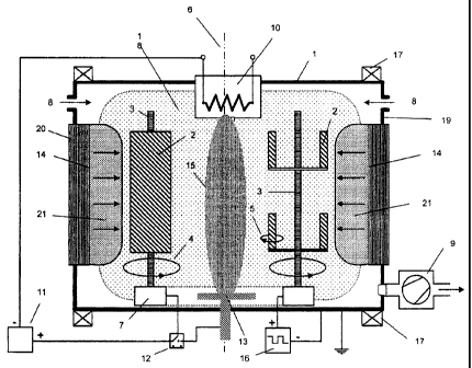
Figure 1 shows a vacuum coating installation with an anode according to prior
art. In
the vacuum chamber 1 the workpieces 2 to be coated are mounted on one or
several
workpiece receptacles 3 comprising means for generating at least a single, if
necessary also double 4 or triple 5, rotation of the parts. The workpiece
receptacles 3
are frequently positioned on a workpiece carrier 7 that can also rotate around
the
installation axis 6.
The different process gases can, via gas feeds 8, be fed into the vacuum
chamber by
means of suitable control devices (not shown).
A high-vacuum capable pump unit 9 is flanged to the chamber.
An ion and/or electron source, in particular an LVA cathode 10, is disposed,
for
example, in the area of the installation axis and connected to the negative
output of an
arc generator 11. Depending on the process step, the positive terminal of the
arc
generator 11 can be connected via a switch 12 to the workpiece carrier 7 or to
the
workpiece receptacle 3 and to the workpieces 2 (heating process) electrically
connected thereto or to the LVA anode 13 (in etching processes or, if
necessary, also
during the coating processes).
One or several vaporizer sources 14, preferably a magnetron or a light arc
vaporizer,
can be provided on the walls of the vacuum chamber I. In another embodiment
(not
shown) of the vaporizer source 14, this source can be disposed as an
anodically
switched crucible centrally in the bottom of the vacuum chamber 1. The
vaporizer
material is converted to the gaseous phase through heating by means of the low-
voltage arc 15.
Further, an additional electric bias generator 16 is provided, with which a
substrate
voltage can be applied to the workpieces.
CA 02686445 2009-11-05
-
WO 2008/145459 14
PCT/EP2008/054851
In addition, electromagnetic coils 17 for the generation of a longitudinal
magnetic
field (a so-called Helmholtz field) penetrating through the plasma volume can
be
disposed on opposite delimitation walls of the vacuum chamber 1 and can be fed
by at
least one but preferably two separate DC voltage sources (not shown),
preferably co-
directional.
As additional measures for boosting or more uniform rendering of the magnetic
field
and, for example, of an MF plasma 18 generated through an MF bias generator,
magnet systems can be located on the side walls 19 of the vacuum chamber 1 in
order
to develop several magnetic near fields 21. In this case, the magnet systems
for near
field generation are preferably at least partially designed as magnetron
magnet
systems 20.
The individual systems of the coating installation are advantageously brought
into
relationship with one another through a process control not further depicted
here.
Figure 2 shows a vacuum coating installation according to the invention with a
simple
graphite anode, in which a graphite covering 22 in the form of a graphite disk
is
placed onto a known flat copper anode.
Since the plasma densities in the low-voltage arc 15 and in its immediate
vicinity are
very high, it is also necessary to protect the workpieces 2 against electric
spark-overs.
This can be done by selecting a suitable substrate voltage. For this reason it
is also not
recommended to work with a bipolar substrate voltage if the discharge currents
are
high, especially if high substrate voltages are to be realized. The reason is
that in
bipolar bias pulse operation very high electron currents can be drawn onto the
workpiece during the positive voltage intervals. At least with DLC and ta-C,
this leads
to undesirable heating of the workpiece, however also to increased spark-overs
onto
the workpiece. The use of a unipolar pulsed substrate voltage, which allows
the
electrons from the low-voltage arc in the pauses to discharge the surface
charge built
up by the positive ions, is much more gentle. In the pulse pauses, workpiece
operation
can be grounded or floating, the latter being even more gentle. However, it
should be
possible to freely form the pulse-pause ratio and it should be possible to
vary it, as
well as the substrate voltage, during the process.
CA 02686445 2013-12-23
In this context it is important that the energy introduction on the workpiece
2 can also be
changed by changing the discharge parameters of the low-voltage arc 15, thus,
for example,
for constant substrate voltage the substrate current, and consequently the
substrate power, can
be changed by increasing or decreasing the discharge current. As stated above,
this method
can also be utilized for multi-layer structures in a layer material of
identical chemical
composition in order to dissipate the tension in thick layers and to obtain
good layer adhesion,
for example.
The low-voltage arc 15 can be formed in two different ways: As shown in the
figures, as a
linear source if the outer coils 17 are utilized for focusing, or as a diffuse
plasma which is
distributed over the entire process chamber such that the workpieces 2 are
immersed in the
plasma.
Figure 3 shows a vacuum treatment installation according to the invention
which, however,
can also be operated as a vacuum treatment installation for PE-CVD processes.
In this
embodiment, the graphite anode is designed as a graphite inlay 22 which is
placed in a known
cooled copper crucible. The latter, in turn, can itself be implemented as a
graphite crucible in
order, for example, to be able to apply in simple manner an adhesive layer by
introducing
metal tablets or the like before the coating with a layer produced by means of
PE-CVD. In
addition, a DC bias generator 16 is utilized in Figure 3.
Figure 4 shows a vacuum coating installation according to the invention with
graphite anode
13, in which two LVA anodes 13 and 23 are disposed. For example, the positive
output of the
arc generator can be connected alternately or simultaneously to the LVA
graphite anode 13,
22 or, in this case, the annular LVA graphite anode 23 via the switch 12.
Similar to operation
without magnet coils, connection of the annular LVA anode 23 allows the plasma
to be
diffusely distributed over the installation chamber 1. It is obvious to
experts in the art that
these two options for optimizing a uniform LVA plasma distribution can be
optimized.
Figure 5 describes by example the course of the process parameters in the
production
of a combined CrN-DLC layer with an interface in between, within which the
CA 02686445 2009-11-05
WO 2008/145459 16
PCT/EP2008/054851
properties of the two different layer systems are essentially continuously
adapted to
one another. First, in a PVD method, for example through a sputter or arc
process, a
CrN layer is generated, while subsequently during the production of the
interface
layer a PE-CVD process is additionally started, and target power and nitrogen
supply
simultaneously decreased to zero. In the last process step, which can also be
applied
directly onto the surface of a workpiece without a preceding intermediate
layer or
interface, constant process parameters are utilized for the production of a
DLC layer
which is isomorphous across the layer thickness.
Figure 6 shows a SEM image of the fracture surface of a multi-layered coating
produced similarly to that in Figure 5, with a chromium adhesive layer,
graduated
interface layer, and DLC cover layer.
Figure 7 depicts a multi-layered coating deposited according to method example
2 of
a sequence of different SiC and DLC layers.
Means for Embodying the Invention
In the following, several examples are described of the process sequence of
the
methods according to the invention.
Examples 1 to 3, which describe methods for the deposition of Si-containing
DLC
layers, were carried out on a modified RCS installation from OC Oerlikon
Balzers
AG, wherein a graphite covering in the shape of a disk was placed on a cooled
copper
anode. This allowed an adequate electric transition to be produced in an
extremely
simple manner. At the same time, the cooling of the graphite surface was
markedly
reduced compared to the original copper anode, thus maintaining the
conductivity of
the surface even during the coating process.
Example 1) Process for the production of DLC with an intermediate layer of
Si/SiC.
After inserting the workpiece into the doubly or triply rotatable holders
provided for
this purpose and introducing the holders into the vacuum treatment
installation, the
treatment chamber is pumped down to a pressure of approximately 104 mbar.
CA 02686445 2009-11-05
WO 2008/145459 17
PCT/EP2008/054851
To set the process temperature, a low-voltage arc (LVA) plasma is ignited in
an argon
hydrogen atmosphere between a cathode chamber separated by an apertured
shutter,
with a hot cathode which forms the LVA cathode, and the anodically switched
workpieces. Preferably, the substrate voltage applied to the workpieces is
additionally
unipolarly or bipolarly pulsed. The standard radiation heaters were not
employed in
this example.
The heating process is based on the following parameters:
Discharge current of the LVA: 50 A
Argon flow: 60 sccm
Hydrogen flow: 300 sccm
Process time: 20 minutes
The next process step, etching, is started. For this, the low-voltage arc is
operated
between the filament and the graphite anode. In principle, a DC, a pulsed DC
or an
AC operated MF or RF supply can be applied between the workpieces and ground.
For the present method a two-stage etching process with the following etching
parameters was set:
Step 1:
Argon flow: 65 sccm
Hydrogen flow: 80 sccm
Discharge current of the LVA: 100 A
Substrate voltage: -50 V unipolar (100 is on/10 vis off)
Process time: 15 minutes
Step 2:
Argon flow: 65 sccm
Hydrogen flow: 80 sccm
Discharge current of the LVA: 100 A
Substrate voltage: -200 V unipolar (100 us on/10 [ts off)
Process time: 30 minutes
CA 02686445 2009-11-05
- WO 2008/145459 1 8
PCT/EP2008/054851
In the next process step, the coating of the workpiece with a DLC layer and an
Si-SiC
intermediate layer was carried out to facilitate adhesion and for adaptation
of the layer
properties to the substrate material. The low-voltage arc is operated for the
coating.
The discharge current of the low-voltage arc is thereby drawn toward the
graphite
anode. The parameters of the low-voltage arc discharge, which occurs during
the
entire coating process, are:
Discharge current of the LVA: 40 A
Argon flow: 60 sccm
For the individual steps of the coating process, the following parameters were
additionally set:
Si adhesion layer:
Silane flow: 30 seem
Substrate voltage: -600 V unipolar (10 pis on/10
!is off)
Duration: 3 minutes
SiC transition layer:
Silane flow: linear ramp from 30 seem to 10
seem
C2H2 flow: linear ramp from 15 seem to 120
seem
Substrate voltage: -600 V unipolar (10 pis on/10
.is off)
Duration: 30 minutes
DLC function layer:
C2H2 flow: 120 seem
Process pressure: 0.36 Pa
Substrate voltage: -600 V unipolar (10 pis on/10
pts off)
Duration: 30 minutes
In this way a layer of approximately 1.5 pIn was deposited. The temperature of
the
workpiece reached approximately 290 C.
CA 02686445 2009-11-05
WO 2008/145459 19
PCT/EP2008/054851
Example 2) In this process, the heating step was omitted and an extended
etching step
was utilized instead. Analogous to the preceding example, the low-voltage arc
is again
operated between the filament and the graphite anode, and a unipolarly pulsed
negative substrate voltage is applied to the workpieces. The following etching
parameters were set:
Step 1:
Argon flow: 65 sccm
Hydrogen flow: 80 sccm
Discharge current of the LVA: 50 A
Bias: -50 V unipolar (100 us on/10 us off)
Process time: 25 minutes
Step 2:
Argon flow: 65 sccm
Hydrogen flow: 80 sccm
Discharge current of the LVA: 100 A
Bias: -150 V unipolar (100 us on/10 us off)
Process time: 60 minutes
In the next process step the coating of the workpiece is carried out with a
DLC-SiC
multi-layered coating and an Si-SiN-SiC intermediate layer. For coating, the
discharge current of the low-voltage arc is drawn toward the graphite anode.
The
parameters of the low-voltage arc discharge are set as in Example 1.
For the individual steps of the coating process, the following parameters were
additionally set:
Si adhesion layer:
Silane flow: 30 scan
Substrate voltage: -600 V unipolar (10 liS on/10 is off)
Duration: 3 minutes
CA 02686445 2009-11-05
= WO 2008/145459
20 PCT/EP2008/05485
SiN transition layer:
Silane flow: 30 sccm
N2 flow: linear ramp from 15 sccm to 120
sccm
Substrate voltage: -600 V unipolar (10 is on/10 ps
off)
Duration: 15 minutes
SiC transition layer:
Silane flow: linear ramp from 30 sccm to 10
sccm
N2 flow: linear ramp from 120 seem to 0
sccm
(within 5 minutes)
C2H2 flow: linear ramp from 15 sccm to 120
sccm
Substrate voltage: -600 V unipolar (10 ps on/10 ps
off)
Duration: 15 minutes
DLC-SiC multi-layer function layer:
C2H2 flow: 120 sccm (for 5 minutes each
time)
Silane flow: 30 sccm (with C2H2 as above for 5
minutes each time)
Process pressure: 0.3 Pa (C2H2) or 0.47 Pa (C2H2 +
SiH4)
Substrate voltage: -600 V unipolar (10 ps on/10 s
off)
Duration: 60 minutes
In this way a total layer thickness of approximately 1.5 pm was attained on
workpieces with double rotation. The temperature of the workpiece reached
approximately 180 C.
Example 3) As in Example 2, in this process the heating step was omitted and
an
extended etching step was employed instead.
In the next process step, the coating of the workpiece was carried out with an
Si-SiC
interlayer, followed by a DLC-Si multi-layered coating and a terminating DLC
layer.
For the coating the low-voltage arc is operated as described in Example 1.
CA 02686445 2009-11-05
WO 2008/145459 21
PCT/EP2008/054851
For the individual steps of the coating process, the following parameters were
additionally set:
Si adhesion layer:
Silane flow: 30 sccm
Substrate voltage: -600 V unipolar (10 jis on/10 jts off)
Duration: 3 minutes
SiC transition layer:
Silane flow: linear ramp from 30 sccm to 10 sccm
C2H2 flow: linear ramp from 15 sccm to 120 sccm
Substrate voltage: -600 V unipolar (10 [is on/10 pis off)
Duration: 30 minutes
DLC-SiC multi-layer function layer:
C2H2 flow: 120 sccm (for 5 minutes each time)
Silane flow: 30 sccm (with C21-17 as above for 5
minutes each time)
Process pressure: 0.3 Pa (C2H2) or 0.43 Pa (C2H2 + SiH4)
Substrate voltage: -600 V unipolar (101AS on/101AS off)
Duration: 60 minutes
For the DLC layer:
C2H2 flow: 120 sccm
Substrate voltage: -800 V unipolar (10 .is on/10 [is off)
Process pressure: 0.3 Pa
Duration: 30 minutes
In this way a total layer thickness of approximately 2 Jim was attained on
workpieces
with double rotation (see Figure 7). The temperature of the workpiece reached
approximately 180 C.
CA 02686445 2009-11-05
' WO 2008/145459 22
PCT/EP2008/054851
Examples 4 to 8, which describe methods for the deposition of DLC layers, were
carried out on a modified BAI830DLC installation from OC Oerlikon Balzers AG.
In
Examples 5 to 6, too, only a graphite covering in the shape of a disk was
placed on a
cooled copper anode. The workpieces were doubly rotated and guided at a
distance of
60-175 mm from the target, at a loading height of 10-1000 mm. Detailed
specifications regarding the particular process parameters as well as the
layer
properties attained can be found in Table I.
Example 4) This example involves a known process for purposes of comparison.
Herein, after heating or etching pretreatment at a process pressure between
5.0x10⁻³
and 2.0x10⁻² mbar, a glow discharge was ignited and operated between workpiece
receptacles and vessel wall, as already described in EP 01362931 or W02006-
116889
Al. The workpiece receptacles are designed such that a hollow cathode
discharge
burns in the interior, boosting the glow discharge plasma. Alternatively,
other
electrically conducting hollow bodies can also be employed for plasma
boosting,
provided that specific geometric conditions, disclosed in W02006-116889 Al,
are
maintained.
Example 5) and Example 7) In these examples according to the invention, a low-
voltage arc discharge is ignited on a graphite anode analogous to Figure 2,
disposed in
the center of a workpiece holder and maintained during the entire process
sequence of
heating, etching and coating. For the DLC coating, two or six sputter sources
equipped with graphite targets are connected, while a DC bias of one hundred
volts is
applied to the workpiece. No hydrocarbon gas was introduced. Because of the
lower
voltage, no hollow discharge is ignited in a holder or a correspondingly built
hollow
body. Therefore, the plasma discharge is far less dependent on the geometry of
the
installed equipment, in particular of the workpiece carrier and the workpiece
receptacles.
Example 6) and Example 8) In these examples, too, according to the invention,
the
process is conducted similarly to Examples 5 and 7 with two or six sputter
targets,
however with, in addition, a small quantity of a hydrocarbon gas added. What
is
remarkable is that, compared to purely sputtered layers, it is thereby
possible to
CA 02686445 2009-11-05
WO 2008/145459 23
PCT/EP2008/054 851
increase the layer hardness by a factor of three to four and thus also the
wear
resistance a great deal.
In spite of the low hardness of the layers deposited without hydrocarbon gas
as per
Examples 5 and 7, these layers can be applied advantageously in order to, for
example, improve the running-in properties and/or slide properties of a hard
layer.
Such a layer system can be particularly simply realized through, for example,
a
combination of the layers from Examples 6 or 8 with layers according to
Examples 5
or 7 deposited thereon.
Another possibility in the above listed sputter processes is, instead of DC
sputtering,
to operate an AC or a pulsed sputter source, for example also as a twin
source, in
which two sputter targets are connected to the counterpole outputs of a
bipolar pulse
generator. In addition, one or several sources connected to an appropriately
designed
sputter generator can also be operated in the method referred to as HIPIMS
(High
Ionization Pulse Impact Magnetron Sputtering) whereby, depending on the
desired
power introduction or target and layer type, a pulse signal is advantageously
applied
to the corresponding source within the following parameter ranges:
Pulse width: 10 [is to 100 ms
Pulse voltage: 100 V to 2 kV
Pulse current: 10 A to 1.5 kA
Pulse power: 5 - 50 kW
CA 02686445 2009-11-05
- WO 2008/145459 24
PCT/EP2008/054851
Table 1
Example 4
Prior Art
Example 5 Example 6 Example 7 Example 8
C2H2[sccm] 220-350 0 10-25 0
10-50
Ar [sccm] 30 - 50 90 90 115
115
Pt.t PO mbar] 5.0-20 3.5 2.9-3.0 3.2
3.2-3.5
ILvA [A] None 30 30 30
30
Sputter sources None 2 2 6
6
Usubstrate pulse[V] 800-1000
50/100/1
Usubstrate DC [V] 100 50/100 100
'substrate [A] 0.5-1 Pi 0 Pi 0.8-1.4 0.8
0.6-1.0
rdeposit [1-im/h] 0.2-0.5 0.1 0.2-0.6 0.8
0.6-1.0
Tsubstrate [T] 200-290 220 200-240 270
210-270
H [At %]1) 13-17 5 12-17 5
11-15
Layer hardness') [H11] 18.500-31.000 4.700 13.700-31.000
4.500 9.500-30.900
Adhesion3) HF 1-2 HF 1-2 HF 1-2 HF 1-2
HF 1-2
Wear4)[m3 m-1 N-' 10-'5] 0.7-1.0 > 6 0.9-5.8 >6
0.4-2.5
0.023 / 0.33 .015-.033 / .084 /
1.48 .027-.058 /
Ra / Rz5) [vim]
.16-.42 .34-.87
1) Hydrogen content, measured by means of SIMS
2) Micro layer hardness according to ISO 14577-1
3) Adhesion according to VDI 3198
4) Wear test according to draft standard DIN EN 1071-6:2006-01 for
determination of the wear resistance of layers
5) Roughness Ra, Rz according to DIN EN ISO 4287/88
CA 02686445 2009-11-05
WO 2008/145459 25
PCT/EP2008/0541
List of reference numbers
1 Vacuum chamber
2 Workpiece
3 Workpiece receptacle
4 Double rotation
Triple rotation
6 Axis of the installation
7 Workpiece carrier
8 Gas feed
9 Pump unit
LVA cathode
11 Arc generator
12 Switch
13 LVA anode
14 Vaporizer source
Low-voltage arc (LVA)
16 Bias generator
17 Electromagnetic coil
18 MF plasma
19 Chamber wall
Magnet system
21 Magnetic near field
22 Graphite covering
23 Annular LVA anode