Note: Descriptions are shown in the official language in which they were submitted.
CA 02686497 2009-12-08
1 1
Low Power Circuit and Driving Method for Emissive Displays
FIELD OF INVENTION
[0001] The present invention relates to a light emitting display, and more
specifically to a
method and system for driving the light emitting display.
BACKGROUND OF THE INVENTION
[0002] Electro-luminance displays have been developed for a wide variety of
devices, such as
cell phones, Personal Digital Assistants (PDAs). Such displays include a
liquid crystal display
( LCD), a field emission display (FED), a plasma display panel (PDP), a light
emitting display
(LED), etc. In particular, active-matrix organic light emitting diode (AMOLED)
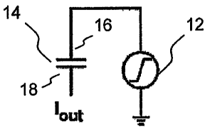
displays with
amorphous silicon (a-Si), poly-silicon, organic, or other driving backplane
have become more
attractive due to advantages, such as feasible flexible displays, its low cost
fabrication, high
resolution, and a wide viewing angle.
[0003] On method employed to drive an emissive display is to program a pixel
directly with
current (e.g., current driven OLED devices). However, a small current required
by OLED,
coupled with a large parasitic capacitance, increases the settling time of the
programming of
the AMOLED display. Furthermore, it is difficult to design an external driver
to provide an
accurate and constant drive current. There is a demand for high resolution
displays with high
aperture ratio or fill factor (defined as the ratio of light emitting display
area to the total pixel
area), ensuring high display quality. There is also a demand of reducing a
size and power
consumption of a device having a display.
[0004] There is a need to provide a display system and its operation method
that can improve
the lifetime, image uniformity, stability and/or yield of the display, and can
provide a high-
resolution stable low power display.
SUMMARY OF THE INVENTION
[0005] It is an object of the invention to provide a method and system that
obviates or
mitigates at least one of the disadvantages of existing systems.
-1-
CA 02686497 2009-12-08
i ,
[0006] According to an aspect of embodiments of the present invention there is
provided a
driver for driving a display system, which includes: a bidirectional current
source for
providing a current to a display system, including: a convertor coupling to a
time-variant
voltage, for converting the time-variant voltage to the current, and a
controller for controlling
the generation of the time-variant voltage.
[0007] According to another aspect of the embodiments of the present invention
there is
provided a pixel circuit, which includes: a transistor for providing a pixel
current to a light
emitting device; and a storage capacitor electrically coupling to the
transistor, the capacitor
coupling to a time-variant voltage in a predetermined timing for providing a
current based on
the time-variant voltage.
[0008] According to a further aspect of the embodiments of the present
invention there is
provided a method of operating a pixel circuit, which includes: in a first
cycle in a
programming operation, changing a time-variant voltage provided to a storage
capacitor in a
pixel circuit, from a reference voltage to a programming voltage, the storage
capacitor
electrically coupling to a driving transistor for driving a light emitting
device; and in a second
cycle in the programming operation, maintaining the time-variant voltage at
the programming
voltage.
[0009] According to a further aspect of the embodiments of the present
invention there is
provided a method of operating a pixel circuit, which includes: in a
programming operation,
providing programming data to a pixel circuit from a data line, the pixel
circuit including a
transistor coupling to the data line and a storage capacitor; and in a driving
operation,
providing, to the storage capacitor in the pixel circuit via a power supply
line, a time-variant
voltage for turning on a light emitting device.
[0010] According to a further aspect of the embodiments of the present
invention there is
provided a pixel circuit, which includes: an organic light emitting diode
(OLED) device
having an electrode and an OLED layer; and an inter-digitated capacitor having
a plurality of
layers, for operating the OLED, the OLED device being disposed on the
plurality of layers,
-2-
CA 02686497 2009-12-08
1 ,
one of the layers of the inter-digitated capacitor being interconnected to the
electrode of the
OLED.
BRIEF DESCRIPTION OF THE DRAWINGS
[0011 ] These and other features of the invention will become more apparent
from the
following description in which reference is made to the appended drawings
wherein:
FIGURE 1 illustrates a bidirectional current source in accordance with an
embodiment of the
disclosure;
FIGURE 2 illustrates an example of a display system with the bidirectional
current source of
Figure 1;
FIGURE 3 illustrates a further example of a display system with the
bidirectional current
source of Figure 1;
FIGURE 4 illustrates a further example of a display system with the
bidirectional current
source of Figure 1;
FIGURE 5 illustrates a further example of a display system with the
bidirectional current
source of Figure 1;
FIGURE 6A illustrates an example of a current biased voltage programmed pixel
circuit
applicable to the display system of Figure 5;
FIGURE 6B illustrates an example of a timing diagram for the pixel circuit of
Figure 6A;
FIGURE 7A illustrates simulation results for the pixel circuit of Figure 6A;
FIGURE 7B illustrates further simulation results for the pixel circuit of
Figure 6A;
FIGURE 8A illustrates a further example of a current biased voltage programmed
pixel
circuit;
FIGURE 8B illustrates an example of a timing diagram for the pixel circuit of
Figure 8A;
-3-
CA 02686497 2009-12-08
i ,
FIGURE 8C illustrates another example of a timing diagram for the pixel
circuit of Figure 8A;
FIGURE 9A illustrates a further example of a current biased voltage programmed
pixel
circuit;
FIGURE 9B illustrates an example of a timing diagram for the pixel circuit of
Figure 9A;
FIGURE 9C illustrates another example of a timing diagram for the pixel
circuit of Figure 9A;
FIGURE I OA illustrates a further example of a current biased voltage
programmed pixel
circuit;
FIGURE I OB illustrates an example of a timing diagram for the pixel circuit
of Figure 10A;
FIGURE 11 A illustrates a further example of a current biased voltage
programmed pixel
circuit;
FIGURE 11 B illustrates an example of a timing diagram for the pixel circuit
of Figure I 1 A;
FIGURE 12A illustrates an example of a display having a current biased voltage
programmed
pixel circuit;
FIGURE 12B illustrates an example of a timing diagram for the display of
Figure 12A;
FIGURE 13A illustrates an example of a display having a current biased voltage
programmed
pixel circuit;
FIGURE 13B illustrates an example of a timing diagram for the display of
Figure 13A;
FIGURE 14A illustrates a further example of a current biased voltage
programmed pixel
circuit;
FIGURE 14B illustrates an example of a timing diagram for the pixel circuit of
Figure 14A;
FIGURE 15A illustrates a further example of a current biased voltage
programmed pixel
circuit;
-4-
CA 02686497 2009-12-08
FIGURE 15B illustrates an example of a timing diagram for the pixel circuit of
Figure 15A;
FIGURE 16 illustrates a further example of a display system having the current
biased voltage
programmed pixel circuit;
FIGURE 17A illustrates an example of a voltage biased current programmed pixel
circuit;
FIGURE 17B illustrates an example of a timing diagram for the pixel circuit of
Figure 17A;
FIGURE 18A illustrates a further example of a voltage biased current
programmed pixel
circuit;
FIGURE 18B illustrates an example of a timing diagram for the pixel circuit of
Figure 18A;
FIGURE 19 illustrates an example of a display system having the voltage biased
current
programmed pixel circuit;
FIGURE 20A illustrates an example of a pixel circuit to which the
bidirectional current source
is applied;
FIGURE 20B illustrates another example of a pixel circuit to which the
bidirectional current
source is applied;
FIGURE 21A illustrates an example of a timing diagram for the pixel circuits
of Figures 20A-
20B;
FIGURE 21 B illustrates another example of a timing diagram for the pixel
circuits of Figures
20A-20B;
FIGURE 22 illustrates a graph showing simulation results (OLED current) for
the pixel
circuits of Figures 20A-20B in one sub-frame for different programming
voltages
FIGURE 23 illustrates a graph showing simulation results (the average current)
for the pixel
circuits of Figures 20A-20B;
-5-
CA 02686497 2009-12-08
FIGURE 24 illustrates a graph showing a power consumption of a 2.2-inch QVGA
panel and
a power consumption used for the OLED;
FIGURE 25 illustrates an example of the implementation of a capacitor for
driving a bottom
emission display;
FIGURE 26 illustrates an example of a layout of the bottom emission pixel;
FIGURE 27 illustrates an example of the implementation of a capacitor for
driving a top
emission display;
FIGURE 28 illustrates an example of a digital to analog convertor (DAC) based
on capacitive
driving;
FIGURE 29 illustrates an example of a timing diagram for the DAC of Figure 28;
FIGURE 30 illustrates another example of a digital to analog convertor (DAC)
based on
capacitive driving; and
FIGURE 31 illustrates an example of a timing diagram for the DAC of Figure 30.
DETAILED DESCRIPTION
[0012] One or more currently preferred embodiments have been described by way
of example.
It will be apparent to persons skilled in the art that a number of variations
and modifications
can be made without departing from the scope of the invention as defined in
the claims.
[0013] Embodiments of the present invention are described using a display
system that may
be fabricated using different fabrication technologies including, for example,
but not limited
to, amorphous silicon, poly silicon, metal oxide, conventional CMOS, organic,
anon/micro
crystalline semiconductors or combinations thereof. The display system
includes a pixel that
may have a transistor, a capacitor and a light emitting device. The transistor
may be
implemented in a variety of materials systems technologies including,
amorphous Si, micro-
/nano-crystalline Si, poly-crystalline Si, organic/polymer materials and
related
-6-
CA 02686497 2009-12-08
nanocomposites, semiconducting oxides or combinations thereof. The capacitor
can have
different structure including metal-insulator-metal and metal-insulator-
semiconductor. The
light emitting device may be, for example, but not limited to, an OLED. The
display system
may be, but not limited to, an AMOLED display system.
[0014] In the description, "pixel circuit" and "pixel" may be used
interchangeably. Each
transistor may have a gate terminal and two other terminals (first and second
terminals). In
the description, one of the terminals or "first terminal" (the other terminal
or "second
terminal") of a transistor may correspond to, but not limited to, a drain
terminal (a source
terminal) or a source terminal (a drain terminal).
[0015] To reduce the fabrication cost, most of fabrication technologies, used
in display
backplane, offer only one type of transistors. Since each type of transistor
is intrinsically good
for uni-directional current source, pixel circuits and/or peripheral driver
circuits become
complicated, resulting in reducing yield, resolution, and aperture ratio. On
the other hand,
capacitance is avaiable in all technology.
[0016] A current driving technique using a differentiator/convertor to convert
a time-variant
voltage to a current is described. In the description, a capacitor is used to
convert a ramp
voltage to a current (e.g., a DC current). Referring to Figure 1, there is
illustrated a current
source developed based on a capacitance. The current source 10 of Figure 1 is
a bidirectional
current source that can provide positive and negative currents. The current
source 10 includes
a voltage generator 12 for generating a time-variant voltage and a driving
capacitor 14. The
voltage generator 12 is coupled to one end terminal 16 of the driving
capacitor 14. A node
"lout" is coupled to the other end terminal 18 of the driving capacitor 14. In
this example, a
ramp voltage is generated by the voltage generator 12. In the embodiments, the
terms
"capacitive current source", "capacitive current source driver", "capacitive
driver" and
"current source" may be used interchangeably. In the embodiments, the terms
"voltage
generator" and "ramp voltage generator" may be used interchangeably. In Figure
1, the
current source 10 includes the ramp voltage generator 12, however, the current
source 10 may
be formed by the driving capacitor 14 that receives the ramp voltage.
-7-
CA 02686497 2009-12-08
[0017] It is assumed that the node "lout" is a virtual ground. A ramp voltage
is applied to the
terminal 16 of the driving capacitor 14, resulting in a fixed current passing
the driving
capacitor 14 and going to lout. i(t)=C dVR(t)/dt (C: Capacitance, VR(t): ramp
voltage).
Amplitude and sign of the ramp's slope are controllable (changeable), which
can change the
value and direction of the output current. Also, the amount of the driving
capacitor 14 can
change the current value. As a result, a digitized capacitance based on the
capacitive current
source 10 can be used to develop a simple and effective current mode analog-to-
digital
convertor (ADC) resulting in small and low power driver. Also it provides a
simple source
driver that can be easily integrated on the panel, independent of fabrication
technology,
resulting in improving the yield and simplicity of the display and reducing
the system cost
significantly.
[0018] In one example, the capacitive current source 10 can be used to provide
a
programming current to a current programmed pixel (e.g., OLED pixels). In
another example,
the capacitive current source 10 can be used to provide a bias current for
accelerating the
programming of a pixel (e.g., current biased voltage programmed pixels in
Figures 8-16 and
voltage biased current programmed pixels in Figures 17-19). In a further
example, the
capacitive current source 10 can be used to drive a pixel. The capacitive
driving technique
with the capacitive current source 10 improves the settling time of the
programming/driving,
which is suitable for larger and higher resolution displays, and thus a low-
power high
resolution emissive display can be realized with the capacitive current source
10, as described
below. The capacitive driving technique with the capacitive current source 10
compensates
for TFT aging (e.g., threshold voltage variations), and thus can improve the
uniformity and
lifetime of the display, as described below.
[0019] In a further example, the capacitive current source 10 may be used with
a current mode
analog-to-digital convertor (ADC), for example, to provide a reference current
to the current
mode ADC where input current is converted to digital signals. In a further
example, the
capacitive driving may be used for a digital to analog convertor (DAC) where
current is
generated based on the ramp voltage and the capacitor.
-8-
CA 02686497 2009-12-08
[0020] Referring to Figure 2, there is illustrated an example of an integrated
display system
with the capacitive driver 10. The integrated display system 20 of Figure 2
includes a pixel
array 22 having a plurality of pixels 24a-24d arranged in columns and rows, a
gate driver 28
for selecting a pixel, and a source driver 27 for providing programming
current to the selected
pixel.
[0021 ] The pixels 24a-24d are current programmed pixel circuits. Each pixel
includes, for
example, a storage capacitor, a driving transistor, a switch transistor (or a
driving and
switching transistor), and a light emitting device. In Figure 2, four pixels
are shown;
however, it would be appreciated by one of ordinary skill in the art that the
number of the
pixels in the pixel array 22 is not limited to four and may vary. The pixel
array 22 may
include a current biased voltage programmed (CBVP) pixel (e.g., Figs. 8-16) or
a voltage
biased voltage programmed (VBCP) pixel (e.g., Figs. 17-19) where the pixel is
operated based
on current and voltage. The CBVP driving technique and the VBCP driving
technique are
suitable for the use in AMOLED displays where they enhance the settling time
of the pixels.
[0022] Each pixel is coupled to an address line 30 and a data line 32. Each
address line 30 is
shared among the pixels in a row. Each data line 32 is shared among the pixels
in a column.
The gate driver 28 drives a gate terminal of the switch transistor in the
pixel via the address
line 30. The source driver 27 includes the capacitive driver 10 for each
column. The
capacitive driver 10 is coupled to the data line 32 in the corresponding
column. The
capacitive driver 10 drives the data line 32. A controller 29 is provided to
control and
schedule programming, calibration, driving and other operations for the
display array 22. The
controller 29 controls the operation of the source driver 27 and the gate
driver 28. Each ramp
voltage generator 12 may be calibrated. In the display system 20, the driving
capacitor 14 is
implemented, for example, on the edge of the display.
[0023] At the beginning of providing a ramp voltage, the capacitance (driving
capacitor 14)
acts as a voltage source and adjusting the voltage of the data line 32. After
the voltage of the
data line 32 reaches a certain proper voltage, the data line 32 acts as a
virtual ground ("lout"
-9-
. . . . ...... _. ...... .._ .... ... ... .. .. . - __... I _.....<_..,...
CA 02686497 2009-12-08
of Figure 1). Thus, the capacitance will act as a current source for providing
a constant
current, after this point. This duality results in a fast settling
programming.
[0024] In Figure 2, the driving capacitor 14 and the storage capacitor of the
pixel are
separately allocated. However, the driving capacitor 14 may be shared with the
storage
capacitor of the pixel as shown in Figure 3.
[0025] Referring to Figure 3, there is illustrated another example of an
integrated display
system with the capacitive driver 10 of Figure 1. The integrated display
system 40 of Figure 3
includes a pixel array 42 having a plurality of pixels 44a-44d arranged in
columns and rows.
The pixels 44a-44d are current programmed pixel circuits, and may be same as
the pixels 24a-
24d of Figure 2. In Figure 3, four pixels are shown; however, it would be
appreciated by one
of ordinary skill in the art that the number of the pixels in the pixel array
42 is not limited to
four and may vary. Each pixel includes, for example, a storage capacitor, a
driving transistor,
a switch transistor (or a driving and switching transistor), and a light
emitting device. For
example, the pixel array 42 may include the pixel of Fig. 6A where the pixel
is operated based
on programming voltage and current bias.
[0026] Each pixel is coupled to the address line 50 and the data line 52. Each
address line 50
is shared among the pixels in a row. A gate driver 48 drives a gate terminal
of the switch
transistor in the pixel via the address line 50. Each data line 52 is shared
among the pixels in
a column, and is coupled to a capacitor 46 in each pixel in the column. The
capacitor 46 in
each pixel in the column is coupled to the ramp voltage generator 12 via the
data line 52. A
source driver 47 includes the ramp voltage generator 12. The ramp voltage
generator 12 is
allocated to each column. A controller 49 is provided to control and schedule
programming,
calibration, driving and other operations for the display array 42. The
controller 49 controls
the gate driver 48 and the source driver 47 having the ramp voltage generator
12. In the
display system 40, the capacitor 46 in the pixel acts as a storage capacitor
for the pixel and
also acts as driving capacitance (capacitor 14 of Figure 1).
-10-
. . ... .. . . ... . . ...... _.... .....:.. . .._ .... _.,.._, -~,..~....
...., ~-...._ _ .......... ......_ I,.,.e..._>.._,.,_..
CA 02686497 2009-12-08
[0027] Referring to Figure 4, there is illustrated a further example of an
integrated display
system with the capacitive driver 10 of Figure 1. The integrated display
system 60 of Figure 4
includes a pixel array 62 having a plurality of pixels 64a-64d arranged in
columns and rows.
In Figure 4, four pixels are shown; however, it would be appreciated by one of
ordinary skill
in the art that the number of the pixels in the pixel array 62 is not limited
to four and may
vary. The pixels 64a-64d are CBVP pixel circuits, each coupling to an address
line 70, a data
line 72, and a current bias line 74. The pixel array 62 may include CBVP
pixels of Figures 8-
16.
[0028] Each address line 70 is shared among the pixels in a row. A gate driver
68 drives a
gate terminal of a switch transistor in the pixel via the address line 70.
Each data line 72 is
shared among the pixels in a column, and is coupled to a source driver 67 for
providing
programming data. The source driver 67 may further provide bias voltage (e.g.,
Vdd of Figure
6). Each bias line 74 is shared among the pixels in a column. The driving
capacitor 14 is
allocated to each column and is coupled to the bias line 74 and the ramp
voltage generator 12.
The ramp voltage generator 12 is shared by more than one column. A controller
69 is
provided to control and schedule programming, calibration, driving and other
operations for
the display array 62. The controller 69 controls the source driver 67, the
gate driver 68, and
the ramp voltage generator 12. In the display system 60, the capacitive
current sources are
easily put on the peripheral of the panel, resulting in reducing the
implementation cost. In
Figure 4, the ramp voltage generator 12 is illustrated separately from the
source driver 67.
However, the source driver 67 may provide the ramp voltage.
[0029] A display system having a CBVP pixel circuit uses voltage to provide
for different
gray scales (voltage programming), and uses a bias to accelerate the
programming and
compensate for the time dependent parameters of a pixel, such as a threshold
voltage shift and
OLED voltage shift. A driver for driving a display array having the CBVP pixel
circuit
converts pixel luminance data into voltage. According to the CBVP driving
scheme, the
overdrive voltage is generated and provided to the driving transistor, which
is independent
from its threshold voltage and the OLED voltage. The shift(s) of the
characteristic(s) of a
pixel element(s) (e.g. the threshold voltage shift of a driving transistor and
the degradation of
-11-
CA 02686497 2009-12-08
a light emitting device under prolonged display operation) is compensated for
by voltage
stored in a storage capacitor and applying it to the gate of the driving
transistor. Thus, the
pixel circuit can provide a stable current though the light emitting device
without any effect of
the shifts, which improves the display operating lifetime. Moreover, because
of the circuit
simplicity, it ensures higher product yield, lower fabrication cost and higher
resolution than
conventional pixel circuits. Since the settling time of the pixel circuits is
much smaller than
conventional pixel circuits, it is suitable for large-area display such as
high definition TV, but
it also does not preclude smaller display areas either. The capacitive driving
technique is
applicable to the CBVP display to further improve the settling time suitable
for larger and
higher resolution displays.
[0030] The capacitive driving technique provides a unique opportunity to share
the current
bias line and voltage data line in CBVP displays. Referring to Figure 5 there
is illustrated a
further example of an integrated display system with the capacitive driver 10
of Figure 1. The
integrated display system 80 of Figure 5 includes a pixel array 82 having a
plurality of pixels
84a-84d arranged in columns and rows. The pixels 84a-84d are CBVP pixel
circuits, and may
be same as the pixels 64a-64d of Figure 4. In Figure 5, four pixels are shown;
however, it
would be appreciated by one of ordinary skill in the art that the number of
the pixels in the
pixel array 82 is not limited to four and may vary. Each pixel is coupled to
the address line 90
and the voltage data/current bias line 92.
[0031] Each address line 90 is shared among the pixels in a row. A gate driver
88 drives a
gate terminal of the switch transistor in the pixel via the address line 90.
Each voltage
data/current bias line 92 is shared among the pixels in a column, and is
coupled to a capacitor
86 in each pixel in the column. The capacitor 86 in each pixel in the column
is coupled to the
ramp voltage generator 12 via the voltage data/current bias line 92. A source
driver 87 has the
ramp voltage generator 12. The ramp voltage generator 12 is allocated to each
column. A
controller 89 is provided to control and schedule programming, calibration,
driving and other
operations for the display array 82. The controller 89 controls the gate
driver 88 and the
source driver 87 having the ramp voltage generator 12. The data voltage and
the biasing
current are carried over through the voltage data/current bias line 92. In the
display system
-12-
CA 02686497 2009-12-08
80, the capacitor 86 in the pixel acts as a storage capacitor for the pixel
and also acts as
driving capacitance (capacitor 14 of Figure 1).
[0032] Referring to Figure 6A, there is illustrated an example of a CBVP pixel
circuit which
is applicable to the pixel of Figure 5. The pixel circuit CBVPOI of Figure 6
includes a driving
transistor 102, a switch transistor 104, a light emitting device 106, and a
capacitor 108. In
Figure 6A, the transistors 102 and 104 are p-type transistors; however, one of
ordinary skill in
the art would appreciate that a CBVP pixel having n-type transistors is also
applicable as the
pixel of Figure 5.
[0033] The gate terminal of the driving transistor 102 is coupled to the
capacitor 108 at BOl .
One of the first and second terminals of the driving transistor 102 is coupled
a power supply
(Vdd) 110 and the other is coupled to the light emitting device 106 at node
A01. The light
emitting device 106 is coupled to a power supply (Vss) 112. The gate terminal
of the switch
transistor 104 is coupled to an address line SEL. One of the first and second
terminals of the
switch transistor 104 is coupled to the gate of the driving transistor 102 and
the other is
coupled to the light emitting device 106 and the driving transistor 102 at
A01. The capacitor
108 is coupled between a data line Vdata and the gate terminal of the driving
transistor 102.
The capacitor 108 acts as a storage capacitor and a capacitive current source
(14 of Figure 1)
as a driver element.
[0034] The capacitor 108 corresponds to the capacitor 86 of Figure 5. The
address line SEL
corresponds to the address line 90 of Figure 5. The data line Vdata
corresponds to the voltage
data/current bias line 92 of Figure 5, and is coupled to the ramp voltage
generator (12 of
Figure 1). The source driver 87 of Figure 5 operates on the data line Vdata to
provide a bias
signal and programming data (Vp) to the pixel.
[0035] In Figure 6A, the ramp voltage is used to carry the bias current while
the initial voltage
of the ramp (Vrefl -Vp) is used to send the programming voltage to the pixel
circuit CBVPO1,
as shown in Figure 6B.
-13-
CA 02686497 2009-12-08
[0036] Referring to Figures 6A and 6B, the operation cycles of the pixel
circuit CBVPOI
includes a programming cycle 120 and a driving cycle 126. The power supply Vdd
coupled to
the driving transistor 102 is low during the programming cycle 120. In the
initial stage 122 of
the programming cycle 120, a ramp voltage is provided to the data line Vdata.
The voltage of
the Vdata goes from (Vrefl -Vp) to Vp where Vp is a programming voltage for
programming
the pixel and Vrefl is a reference voltage. During the initial stage 122, the
address line SEL is
set to a low voltage so that the switch transistor 104 is on. During the
initial stage 122, the
capacitor 108 acts as a current source. The voltage of node A01 goes to VBTI
where VB is a
function of T1's characteristics (T1: the driving transistor 102) and the
voltage of node B01
goes to VBTI + VrT2 where VrT2 is the voltage drop across T2 (T2: the switch
transistor 104)
[0037] At the next stage 124 after the initial stage 122, the voltage of Vdata
remains Vp, and
the address line SEL goes high to render the switch transistor 104 off. During
the stage 124,
the capacitor 108 acts as a storage element. During the driving cycle 126, the
data line Vdata
goes to Vref2 and stay at Vref2 for the rest of the frame.
[0038] Vrefl defines the level of bias current Ibias and it is determined, for
example, based on
TFT, OLED, and display characteristics and specifications. Vref2 is a function
of Vrefl and
pixel characteristics.
[0039] Referring to Figures 7A-7B, there are illustrated graphs showing
simulation results for
the pixel circuit of Figure 6A using the operation of Figure 6B. In Figure 7A,
"OVT"
represents variation of driving transistor threshold VT, and " " represents
mobility (cm2N.s).
As shown in Figures 7A-7B, despite variation in the driving transistor
threshold VT and
mobility, the pixel current is stable for all gray scales.
[0040] Referring to Figs. 8-16, there are illustrated examples of CBVP pixel
circuits, which
may form the pixel arrays of Figures 2-5. In Figures 8-16, a current bias line
("Ibias" or
"IBIAS") provides a bias current to the corresponding pixel. The capacitive
driver 10 of
Figure 1 may provide a constant bias current to the current bias line.
Examples of the CBVP
pixels, display systems and operations are disclosed in US Patent Application
Publication
-14-
CA 02686497 2009-12-08
US2006/0125408 and PCT International Application Publication W02009/127065,
which are
hereby incorporated by reference.
[0041] A pixel circuit CBVPO2 of Figure 8A includes an OLED 210, a storage
capacitor 212 ,
a driving transistor 214, and switch transistors 216 and 218. The transistors
214 , 216 and 218
are n-type TFT transistors. One of ordinary skill in the art would appreciate
a circuit that is
complementary to the pixel circuit CBVPO2 and has p-type transistors. Two
select lines SEL1
and SEL2, a signal line VDATA, a bias line IBIAS, a voltage supply line VDD,
and a
common ground are coupled to the pixel circuit CBVPO2. In Figure 8A, the
common ground
is for the OLED top electrode. The common ground is not a part of the pixel
circuit, and is
formed at the final stage when the OLED 210 is formed. The transistors 214 and
216 and the
storage capacitor 212 are connected to node A11. The OLED 210, the storage
capacitor 212
and the transistors 214 and 218 are connected to node B 11.
[0042] The gate terminal of the driving transistor 214 is connected to the
signal line VDATA
through the switch transistor 216 and the capacitor 212. One of the first and
second terminals
of the driving transistor 214 is connected to the voltage supply line VDD, and
the other is
connected to the anode electrode of the OLED 210 at B 11. The storage
capacitor 212 is
connected between the gate terminal of the driving transistor 214 at A11 and
the OLED 210 at
B1 l. The gate terminal of the switch transistor 216 is connected to the first
select line SEL1.
One of the first and second terminals of the switch transistor 216 is
connected to the signal
line VDATA, and the other is connected to the gate terminal of the driving
transistor 214 at
A11. The gate terminal of the switch transistor 218 is connected to the second
select line
SEL2. One of the first and second terminals of the switch transistor 218 is
connected to the
anode electrode of the OLED 210 and the storage capacitor 212 at B 11, and the
other is
connected to the bias line IBIAS. The cathode electrode of the OLED 210 is
connected to the
common ground.
[0043] The operation of the pixel circuit CBVPO2 includes a programming phase
having a
plurality of programming cycles, and a driving phase having one driving cycle.
During the
-15-
CA 02686497 2009-12-08
programming phase, node B11 is charged to negative of the threshold voltage of
the driving
transistor 214, and node A11 is charged to a programming voltage VP.
[0044] As a result, the gate-source voltage of the driving transistor 214 is:
VGS=VP-(-VT)=VP+VT (1)
where VGS represents the gate-source voltage of the driving transistor 214,
and VT represents
the threshold voltage of the driving transistor 214. This voltage remains on
the capacitor 212
in the driving phase, resulting in the flow of the desired current through the
OLED 210 in the
driving phase.
[0045] Referring to Figure 8B, there is illustrated one exemplary operation
process applied to
the pixel circuit CBVPO2 of Figure 8A. In Figure 8B, "VnodeB" represents
voltage at node
B11 of Figure 8A, "VnodeA" represents voltage at node A11 of Figure 8A,
"VSEL1"
corresponds to SEL1 of Figure 8A, and "VSEL2" corresponds to SEL2 of Figure
8A. The
programming phase has two operation cycles X11, X12, and the driving phase has
one
operation cycle X13.
[0046] The first operation cycle X11: Both select lines SEL1 and SEL2 are
high. A bias
current IB flows through the bias line IBIAS, and VDATA goes to a bias voltage
VB.
[0047] As a result, the voltage of node B11 is:
-16-
CA 02686497 2009-12-08
VnodeB = VB - F VT (2)
where VnodeB represents the voltage of node B 11, VT represents the threshold
voltage of the
driving transistor 214, and (3 represents the coefficient in current-voltage
(I-V)
characteristics of the TFT given by IDS =~3 (VGS - VT)2. IDS represents the
drain-source
current of the driving transistor 214.
[0048] The second operation cycle X12: While SEL2 is low, and SELl is high,
VDATA goes
to a programming voltage VP. Because the capacitance 211 of the OLED 210 is
large, the
voltage of node B I 1 generated in the previous cycle stays intact.
[0049] Therefore, the gate-source voltage of the driving transistor 214 can be
found as:
VGS=VP+dVB+VT (3)
AVB = ~ (4)
[0050] AVB is zero when VB is chosen properly based on (4). The gate-source
voltage of the
driving transistor 214, i.e., VP+VT, is stored in the storage capacitor 212.
[0051] The third operation cycle X13: IBIAS goes to low. SEL1 goes to zero.
The voltage
stored in the storage capacitor 212 is applied to the gate terminal of the
driving transistor 214.
The driving transistor 214 is on. The gate-source voltage of the driving
transistor 214
develops over the voltage stored in the storage capacitor 212. Thus, the
current through the
OLED 210 becomes independent of the shifts of the threshold voltage of the
driving transistor
and OLED characteristics.
[0052] Referring to Figure 8C, there is illustrated a further exemplary
operation process
applied to the pixel circuit CBVPO2 of Figure 8A. In Figure 8C, "VnodeB"
represents voltage
at node B11 of Figure 8A, "VnodeA" represents voltage at node A11 of Figure
8A, "VSELl"
corresponds to SEL1 of Figure 8A, and "VSEL2" corresponds to SEL2 of Figure
8A. The
-17-
CA 02686497 2009-12-08
programming phase has two operation cycles X21, X22, and the driving phase has
one
operation cycle X23. The first operation cycle X21 is same as the first
operation cycle XI 1 of
Figure 8B. The third operation cycle X23 is same as the third operation cycle
X 13 of Figure
8B. In Figure 8C, the select lines SEL1 and SEL2 have the same timing. Thus,
SELl and
SEL2 may be connected to a common select line.
[0053] The second operating cycle X22: SEL1 and SEL2 are high. The switch
transistor 218
is on. The bias current IB flowing through IBIAS is zero.
[0054] The gate-source voltage of the driving transistor 214 can be VGS = VP +
VT as
described above. The gate-source voltage of the driving transistor 214, i.e.,
VP+VT, is stored
in the storage capacitor 212.
[0055] A pixel circuit CBVPO3 of Figure 9A is complementary to the pixel
circuit CBVPO2
of Figure 8A, and has p-type transistors. The pixel circuit CBVPO3 includes an
OLED 220, a
storage capacitor 222, a driving transistor 224, and switch transistors 226
and 228. The
transistors 224, 226 and 228 are p-type transistors. Two select lines SEL1 and
SEL2, a signal
line VDATA, a bias line IBIAS, a voltage supply line VDD, and a common ground
are
coupled to the pixel circuit CBVPO3.
[0056] The transistors 224 and 226 and the storage capacitor 222 are connected
at A12. The
cathode electrode of the OLED 220, the storage capacitor 222 and the
transistors 224 and 228
are connected at B12. Since the OLED cathode is connected to the other
elements of the pixel
circuit CBVPO3, this ensures integration with any OLED fabrication.
[0057] Referring to Figures 9B-9C, there are illustrated exemplary operation
processes
applied to the pixel circuit CBVPO3 of Figure 9A. Figure 9B corresponds to
Figure 8B.
Figure 9C corresponds to Figure 8C. The CBVP driving schemes of Figures 9B-9C
use
IBIAS and VDATA similar to those of Figures 8B-8C.
[0058] A pixel circuit CBVPO4 of Figure l0A includes an OLED 230, storage
capacitors 232
and 233, a driving transistor 234, and switch transistors 236, 238 and 240.
The transistors
-18-
CA 02686497 2009-12-08
234, 236, 238 and 240 are n-type TFT transistors. One of ordinary skill in the
art would
appreciate a circuit that is complementary to the pixel circuit CBVPO4 and has
p-type
transistors. A select line SEL, a signal line VDATA, a bias line IBIAS, a
voltage line VDD,
and a common ground are coupled to the pixel circuit CBVPO4. The OLED 230, the
transistors 234, 236 and 240 are connected at node A21. The storage capacitor
232 and the
transistors 234 and 236 are connected at node B21.
[0059] One of the first and second terminals of the driving transistor 234 is
connected to the
cathode electrode of the OLED 230 at A21, and the other is connected to a
ground potential.
The storage capacitors 232 and 233 are in series and connected between the
gate of the driving
transistor 234 at B21 and the ground. The gate terminals of the switch
transistors 236, 238
and 240 are connected to the select line SEL. One of the first and second
terminals of the
switch transistor 236 is connected to the OLED 230 and the driving transistor
234 at A21, and
the other is connected to the gate terminal of the driving transistor 234 at
B21. One of the
first and second terminals of the switch transistor 238 is connected to the
signal line VDATA,
and the other is connected to C21 connecting the storage capacitors 232 and
233. One of the
first and second terminals of the switch transistor 240 is connected to the
bias line IBIAS, and
the other is connected to the cathode terminal of the OLED 230 as A21. The
anode electrode
of the OLED 230 is connected to the VDD.
[0060] The operation of the pixel circuit CBVPO4 includes a programming phase
having a
plurality of programming cycles, and a driving phase having one driving cycle.
During the
programming phase, the first storage capacitor 232 is charged to a programming
voltage VP
plus the threshold voltage of the driving transistor 234, and the second
storage capacitor 233
is charged to zero.
[0061] As a result, the gate-source voltage of the driving transistor 234 is:
-19-
CA 02686497 2009-12-08
VGS= VP+VT (5)
where VGS represents the gate-source voltage of the driving transistor 234,
and VT represents
the threshold voltage of the driving transistor 234.
[0062] Referring to Figure l OB, there is illustrated one exemplary operation
process applied
to the pixel circuit CBVPO4 of Figure 10A. The programming phase has two
operation cycles
X31, X32, and the driving phase has one operation cycle X33.
[0063] The first operation cycle X3 1: The select line SEL is high. A bias
current IB flows
through the bias line IBIAS, and VDATA goes to a VB-VP where VP is and
programming
voltage and VB is given by:
(6)
VB = F,8
[0064] As a result, the voltage stored in the first capacitor 232 is:
VC1 = VP + VT (7)
where VC1 represents voltage stored in the first storage capacitor 232, VT
represents the
threshold voltage of the driving transistor 234, (3 represents the coefficient
in current-voltage
(I-V) characteristics of the TFT given by IDS =(3(VGS -VT)2. IDS represents
the drain-
source current of the driving transistor 234.
[0065] The second operation cycle X32: While SEL is high, VDATA is zero, and
IBIAS goes
to zero. Because the capacitance 231 of the OLED 230 and the parasitic
capacitance of the
bias line IBIAS are large, the voltage at node B21 and the voltage at node A21
generated in
the previous cycle stay unchanged.
[0066] Therefore, the gate-source voltage of the driving transistor 234 can be
found as:
-20-
CA 02686497 2009-12-08
VGS=VP+VT (8)
where VGS represents the gate-source voltage of the driving transistor 234.
The gate-source
voltage of the driving transistor 234 is stored in the storage capacitor 232.
[0067] The third operation cycle X33: IBIAS goes to zero. SEL goes to zero.
The voltage of
node C21 goes to zero. The voltage stored in the storage capacitor 232 is
applied to the gate
terminal of the driving transistor 234. The gate-source voltage of the driving
transistor 234
develops over the voltage stored in the storage capacitor 232. Considering
that the current of
driving transistor 234 is mainly defined by its gate-source voltage, the
current through the
OLED 230 becomes independent of the shifts of the threshold voltage of the
driving transistor
234 and OLED characteristics.
[0068] A pixel circuit CBVPO5 of Figure 11A is complementary to the pixel
circuit CBVPO4
of Figure 10A, and has p-type transistors. The pixel circuit CBVPO5 includes
an OLED 250, a
storage capacitors 252 and 253, a driving transistor 254, and switch
transistors 256, 258 and
260. The transistors 254, 256, 258 and 260 are p-type transistors. Two select
lines SEL1 and
SEL2, a signal line VDATA, a bias line IBIAS, a voltage supply line VDD, and a
common
ground are coupled to the pixel circuit CBVPO5. The common ground may be same
as that of
Figure 8A.
[0069] The anode electrode of the OLED 250, the transistors 254, 256 and 260
are connected
at node A22. The storage capacitor 252 and the transistors 254 and 256 are
connected at node
B22. The switch transistor 258, and the storage capacitors 252 and 253 are
connected at node
C22.
[0070] Referring to Figure 11 B, there is illustrated one exemplary operation
process applied
to the pixel circuit CBVPO5 of Figure 11A. Figure 11B corresponds to Figure
IOB. As
shown in Figure 11B, the CBVP driving scheme of Figure 11B uses IBIAS and
VDATA
similar to those of Figure I OB.
-21-
CA 02686497 2009-12-08
[0071 ] A display having a CBVP pixel circuit in Figure 12A is based on the
pixel circuit
CBVPO4 of Figure 10A, and includes an OLED 270, storage capacitors 272 and
274, and
transistors 276, 278, 280, 282 and 284. The transistor 276 is a driving
transistor. The
transistors 278, 280 and 284 are switch transistors. The transistors 276 and
280 and the
storage capacitor 272 are connected at node A3 1. The transistors 282 and 284
and the storage
capacitors 272 and 274 are connected at B31. The gate terminals of the
transistors 278, 280
and 282 are coupled to an address line SEL[n] for the nth row, and the gate
terminal of the
switch transistor 284 is coupled to an address line SEL[n+1] for the (n+1)th
row. The
transistors 276 , 278 , 280, 282 and 284 are n-type TFT transistors. One of
ordinary skill in
the art would appreciate a circuit that is complementary to the pixel circuit
of Figure 12A and
has p-type transistors. One of ordinary skill in the art would appreciate that
the driving
technique applied to Figure 12A is applicable to the complementary pixel
circuit. In Figure
12A, elements associated with two rows and one column are shown. The display
of Figure
12A may include more than two rows and more than one column.
[0072] Referring to Figure 12B, there is illustrated one exemplary operation
process applied
to the display of Figure 12A. In Figure 12B, "Programming cycle [n]"
represents a
programming cycle for the row [n] of the display. The programming time is
shared between
two consecutive rows (n and n+1). During the programming cycle of the nth row,
SEL[n] is
high, and a bias current IB is flowing through the transistors 278 and 280.
The voltage at
node A31 is self-adjusted to (IB/0)1/2+VT, while the voltage at node B31 is
zero, where VT
represents the threshold voltage of the driving transistor 276, and 0
represents the coefficient
in current-voltage (I-V) characteristics of the TFT given by IDS =(3 (VGS -
VT)Z, and IDS
represents the drain-source current of the driving transistor 276.
[0073] During the programming cycle of the (n+l)th row, VDATA changes to VP-
VB. As a
result, the voltage at node A31 changes to VP+VT if VB =(IB/(3)1/2. Since a
constant current
is adopted for all the pixels, the IBIAS line consistently has the appropriate
voltage so that
there is no necessity to pre-charge the line, resulting in shorter programming
time and lower
power consumption. More importantly, the voltage of node B31 changes from VP-
VB to zero
at the beginning of the programming cycle of the nth row. Therefore, the
voltage at node A31
-22-
CA 02686497 2009-12-08
changes to (IB/0)1/2+VT, and it is already adjusted to its final value,
leading to a fast settling
time.
[0074] A display having a CBVP pixel circuit in Figure 13A is based on the
pixel circuit
CBVPO5 of Figure 11, and has OLED 290, a storage capacitors 292 and 294, and p-
type TFT
transistors 296, 298, 300, 302 and 304. The transistor 296 is a driving
transistor. The
transistors 298, 300 and 304 are switch transistors. The transistors 296 and
300 and the
storage capacitor 292 are connected at node A32. The transistors 302 and 304
and the storage
capacitors 292 and 294 are connected at B32. The transistors 296, 298 and 200
and the OLED
290 are connected at C32. The gate terminals of the transistors 298, 300 and
302 are coupled
to an address line SEL[n] for the nth row, and the gate terminal of the switch
transistor 304 is
coupled to an address line SEL[n+l] for the (n+1)th row. One of ordinary skill
in the art
would appreciate a circuit that is complementary to the pixel circuit of
Figure 13A and has n-
type transistors. One of ordinary skill in the art would appreciate that the
driving technique
applied to Figure 13A is applicable to the complementary pixel circuit. In
Figure 13A,
elements associated with two rows and one column are shown. The display of
Figure 13A
may include more than two rows and more than one column. The driving
transistor 296 is
connected between the anode electrode of the OLED 290 and a voltage supply
line VDD.
[0075] Referring to Figure 13B, there is illustrated one exemplary operation
process applied
to the display of Figure 13A. Figure 13B corresponds to Figure 12B. The CBVP
driving
scheme of Figure 13B uses IBIAS and VDATA similar to those of Figure 12B.
[0076] A pixel circuit CBVPO6 of Figure 14A includes an OLED 322, a storage
capacitor
324, a driving transistor 326, and switch transistors 328 and 330. The
transistors 326, 328 and
330 are p-type TFT transistors. One of ordinary skill in the art would
appreciate a circuit that
is complementary to the pixel circuit of Figure 14A and has n-type
transistors. One of
ordinary skill in the art would appreciate that the driving technique applied
to Figure 14A is
applicable to the complementary pixel circuit. A select line SEL, a signal
line Vdata, a bias
line Ibias, and a voltage supply line Vdd are connected to the pixel circuit
CBVPO6. The bias
- 23 -
CA 02686497 2009-12-08
line Ibias provides a bias current (Ibias) that is defined based on display
specifications, such as
lifetime, power, and device performance and uniformity.
[0077] One of the first and second terminals of the driving transistor 326 is
connected to the
voltage supply line Vdd, and the other is connected to the OLED 322 at node
B40. One
terminal of the capacitor 324 is connected to the signal line Vdata, and the
other terminal is
connected to the gate terminal of the driving transistor 326 at node A40. The
gate terminals of
the switch transistors 328 and 330 are connected to the select line SEL. The
switch transistor
328 is connected between A40 and B40. The switch transistor 330 is connected
between B40
and the bias line Ibias. In the pixel circuit CBVPO6, a predetermined fixed
current (Ibias) is
provided through the transistor 330 to compensate for all spatial and temporal
non-
uniformities and voltage programming is used to divide the current in
different current levels
required for different gray scales.
[0078] Referring to Figure 14B, there is illustrated one exemplary operation
process applied
to the pixel circuit CBVPO6 of Figure 14A. The operation process includes a
programming
phase X61 and a driving phase X62. Vdata [j] in Figure 14B corresponds to
Vdata of Figure
14A. Vp[k,j] in Figure 14B (k=1, 2, ..., n) represents the kth programming
voltage on Vdata
[j] where "j" is the column number. SEL[j] in Figure 14B (j=1, 2, ...)
represents a select line
("SEL" in Figure 14A) for the jth column.
[0079] During the programming cycle X61, SEL is low so that the switch
transistors 328 and
330 are on. The bias current Ibias is applied via the bias line Ibias to the
pixel circuit
CBVPO6, and the gate terminal of the driving transistor 326 is self-adjusted
to allow all the
current passes through source-drain of the driving transistor 326. At this
cycle, Vdata has a
programming voltage related to the gray scale of the pixel. During the driving
cycle X62, the
switch transistors 328 and 330 are off, and the current passes through the
driving transistor
326 and the OLED 322.
[0080] A pixel circuit CBVPO7 of Figure 15A includes an OLED 342, a storage
capacitor
344, and transistors 346, 358, 360, 362, 364, and 366. The transistors 346,
358, 360, 362,
-24-
CA 02686497 2009-12-08
364, and 366 are p-type TFT transistors. One of ordinary skill in the art
would appreciate a
circuit that is complementary to the pixel circuit of Figure 15A and has n-
type transistors.
One of ordinary skill in the art would appreciate that the driving technique
applied to Figure
15A is applicable to the complementary pixel circuit. One select line SEL, a
signal line
Vdata, a bias line Ibias, a voltage supply line Vdd, a reference voltage line
Vref, and an
emission signal line EM are connected to the pixel circuit CBVPO7. The bias
line Ibias
provides a bias current (Ibias) that is defined based on display
specifications, such as lifetime,
power, and device performance and uniformity. The reference voltage line Vref
provides a
reference voltage (Vref). The reference voltage Vref may be determined based
on the bias
current Ibias and the display specifications that may include gray scale
and/or contrast ratio.
The signal line EM provides an emission signal EM that turns on the pixel
circuit CBVPO7.
The pixel circuit CBVPO7 goes to emission mode based on the emission signal
EM. The
select line SEL is connected to the gate terminals of the transistors 358, 360
and 362. The
select line EM is connected to the gate terminals of the transistors 364 and
366. The transistor
346 is a driving transistor. The transistors 358, 360, 362, 364, and 366 are
switching
transistors.
[0081 ] One of the first and second terminals of the transistor 362 is
connected to the reference
voltage line Vref, and the other is connected to the gate terminal of the
transistor 346 at node
A41. One of the first and second terminals of the transistor 364 is connected
to A41 and the
other is connected to the capacitor 344 at B41. One of the first and second
terminals of the
transistor 358 is connected to Vdata and the other is connected to B41. One of
the first and
second terminals of the transistor 366 is connected to Vdd and the other is
connected to the
capacitor 344 and the transistor 346 at C41. One of the first and second
terminals of the
transistor 360 is connected to Ibias and the other is connected to the
capacitor 344 and the
transistor 346 at C41. One of the first and second terminals of the transistor
346 is connected
to OLED 342 and the other is connected to the capacitor 344 and the
transistors 366 and 360
at C41.
[0082] In the pixel circuit CBVPO7, a predetermined fixed current (Ibias) is
provided through
the transistor 360 while the reference voltage Vref is applied to the gate
terminal of the
- 25 -
CA 02686497 2009-12-08
transistor 346 through the transistor 362 and a programming voltage VP is
applied to the other
terminal of the storage capacitor 344 (i.e., node B41) through the transistor
358. Here, the
source voltage of the transistor 346 (i.e., voltage of node C41) will be self-
adjusted to allow
the bias current goes through the transistor 346 and thus it compensates for
all spatial and
temporal non-uniformities. Also, voltage programming is used to divide the
current in
different current levels required for different gray scales.
[0083] Referring to Figure 15B, there is illustrated one exemplary operation
process applied
to the pixel circuit CBVPO7 of Figure 15A. The operation process includes a
programming
phase X71 and a driving phase X72. During the programming cycle X71, SEL is
low so that
the transistors 358, 360 and 362 are on, a fixed bias current is applied to
Ibias line, and the
source of the transistor 346 is self-adjusted to allow all the current passes
through source-
drain of the transistor 346. At this cycle, Vdata has a programming voltage
related to the gray
scale of the pixel and the capacitor 344 stores the programming voltage and
the voltage
generated by current for mismatch compensation. During the driving cycle X72,
the
transistors 358, 360 and 362 are off, while the transistors 364 and 366 are on
by the emission
signal EM. During this driving cycle X72, the transistor 346 provides current
for the OLED
342.
[0084] In Figure 14B, the entire display is programmed, then it is light up
(goes to emission
mode). By contrast, in Figure 15B, each row can light up after programming by
using the
emission line EM.
[0085] In the above examples of Figures 8-15, the capacitor of each pixel may
act as the
storage capacitor and the driving capacitor 14 of Figure 1. In the above
examples, the
capacitive current source 10 of Figure 1 is used to provide a constant current
to the bias
current line. In another example, the capacitive current source 10 may adjust
the bias current
during the operation of the display.
[0086] Referring to Figure 16, there is illustrated a further example of a
display system having
array structure for implementation of the CBVP driving scheme. The display
system 370 of
-26-
CA 02686497 2009-12-08
Figure 16 includes a pixel array 372 having a plurality of pixels 374, a gate
driver 376, a
source driver 378, and a controller 380. The controller 380 is provided to
control and
schedule programming, calibration, driving and other operations for the
display array 372,
which include the CBVP driving scheme and the capacitive driving as described
above. The
controller 380 controls the drivers 376 and 378. The pixel circuit 374 is a
current biased
voltage programmed pixel (e.g., of Figures 8-15) where SEL [i] (i=l, 2, ...)
is a select
(address) line (e.g., SEL), Vdata [j] (j=1, 2, ...) is a signal (data) line
(e.g., Vdata, VDATA),
and Ibias [j] (j=1, 2, ...) is a bias line (e.g., Ibias, IBIAS). The gate
driver 376 operates on the
address (select) lines (e.g., SEL [1], SEL[2], ...). The source driver 378
operates on the data
lines (e.g., Vdata [1], Vdata [2], ...). When using the pixel circuit CBVPO7
of Figure 15A as
the pixel circuit 374, a driver at the peripheral of the display, such as the
gate driver 376,
controls each emission line EM.
[0087] The display system 370 includes a calibrated current mirrors block 382
for operating
on the bias lines (e.g., Ibias [1], Ibias [2]) using a reference current Iref.
The block 382
includes a plurality of calibrated current mirrors, each for the corresponding
Ibias. The
reference current Iref may be provided to the calibrated current mirrors block
382 through a
switch.
[0088] In Figure 16, the current mirrors are calibrated with a reference
current source. During
the programming cycle of the panel (e.g., X61 of Figure 14B, X71 of Figure
15B), the
calibrated current mirrors (block 382) provide current to the bias line Ibias.
These current
mirrors can be fabricated at the edge of the panel. The capacitive driver 10
of Figure 1 may
generate the reference current Iref in Figure 16.
[0089] The shift(s) of the characteristic(s) of a pixel element(s) (e.g. the
threshold voltage
shift of a driving transistor and the degradation of a light emitting device
under prolonged
display operation) is compensated for by voltage stored in a storage capacitor
and applying it
to the gate of the driving transistor. Thus, the pixel circuit can provide a
stable current though
the light emitting device without any effect of the shifts, which improves the
display operating
lifetime. Moreover, because of the circuit simplicity, it ensures higher
product yield, lower
-27-
CA 02686497 2009-12-08
fabrication cost and higher resolution than conventional pixel circuits. Since
the settling time
of the pixel circuits described above is much smaller than conventional pixel
circuits, it is
suitable for large-area display such as high definition TV, but it also does
not preclude smaller
display areas either.
[0090] Referring to Figs. 17-19, there are illustrated examples of VBCP pixel
circuits, which
may form the pixel arrays of Figure 2-5. Examples of the VBCP pixels, their
display systems
and operations are disclosed in US Patent Application Publication
US2006/0125408 and PCT
International Application Publication W02009/127065, which are hereby
incorporated by
reference.
[0091] In the VBCP driving scheme, a pixel current is scaled down without
resizing mirror
transistors. The VBCP driving scheme uses current to provide for different
gray scales
(current programming), and uses a bias to accelerate the programming and
compensate for a
time dependent parameter of a pixel, such as a threshold voltage shift. One of
the terminals of
a driving transistor is connected to a virtual ground VGND. By changing the
voltage of the
virtual ground, the pixel current is changed. A bias current IB is added to a
programming
current IP at a driver side, and then the bias current is removed from the
programming current
inside the pixel circuit by changing the voltage of the virtual ground. A
driver for driving a
display array having the VBCP pixel circuit converts pixel luminance data into
current.
[0092] The capacitive driving technique is applicable to the VBCP display to
further improve
the settling time suitable for larger and higher resolution displays. In
Figures 17-19, a data
line IDATA provides the programming current IP and the bias current IB to the
corresponding
pixel where the capacitive driver 10 of Figure 1 is used, for example, to
provide the bias
current IB.
[0093] A pixel circuit VBCPOI of Figure 17A includes an OLED 410, a storage
capacitor
411, a switch network 412, and mirror transistors 414 and 416. The mirror
transistors 414 and
416 form a current mirror where the transistor 414 is a programming transistor
and the
transistor 416 is a driving transistor. The switch network 412 includes switch
transistors 418
-28-
CA 02686497 2009-12-08
and 420. The transistors 414, 416, 418 and 420 are n-type TFT transistors. One
of ordinary
skill in the art would appreciate a circuit that is complementary to the pixel
circuit VBCPO 1
and has p-type transistors. A select line SEL, a signal line IDATA, a virtual
grand line
VGND, a voltage supply line VDD, and a common ground are connected to the
pixel circuit
VBCPO1.
[0094] One of the first and second terminals of the transistor 416 is
connected to the cathode
electrode of the OLED 410 and the other is connected to the VGND. The gate
terminal of the
transistor 414, the gate terminal of the transistor 416, and the storage
capacitor 411 are
connected at node A5 1. The gate terminals of the switch transistors 418 and
420 are connected
to the SEL. One of the first and second terminals of the switch transistor 418
is connected to
the gate terminal of the transistor 416 at A51 and the other is connected to
the transistor 414.
One of the first and second terminals of the switch transistor 420 is
connected to the IDATA
and the other is connected to the transistor 414.
[0095] Referring to Figure 17B, there is illustrated an exemplary operation
for the pixel
circuit VBCPO 1 of Figure 17A. Referring to Figures 17A and 17B, current
scaling technique
applied to the pixel circuit VBCPO1 is described in detail. The operation of
the pixel circuit
VBCPO 1 has a programming cycle X81 and a driving cycle X82.
[0096] The programming cycle X81: SEL is high. Thus, the switch transistors
418 and 420
are on. The VGND goes to a bias voltage VB. A current (IB+IP) is provided
through the
IDATA, where IP represents a programming current, and IB represents a bias
current. A
current equal to (IB+IP) passes through the switch transistors 418 and 420.
[0097] The gate-source voltage of the driving transistor 416 is self-adjusted
to:
-29-
CA 02686497 2009-12-08
VGS = fIP~IB +VT (9)
where VT represents the threshold voltage of the driving transistor 416, and
(3 represents the
coefficient in current-voltage (I-V) characteristics of the TFT given by IDS
=(3(VGS -VT)2.
IDS represents the drain-source current of the driving transistor 416.
[0098] The voltage stored in the storage capacitor 411 is:
VCS = /IP+JBVB+VT (10)
where VCS represents the voltage stored in the storage capacitor 411.
[0099] Since one terminal of the driving transistor 416 is connected to the
VGND, the current
flowing through the OLED 410 during the programming time is:
Ipixel =IP+IB+,l3=(VB)2 -2~,8 =VB (IP+IB) (11)
where Ipixel represents the pixel current flowing through the OLED 410.
[00100] If IB >> IP, the pixel current Ipixel can be written as:
Ipixel =IP+(IB+8 =(VB)2 -2~fi =VB= IB) (12)
[00101] VB is chosen properly as follows:
VB = IB (13)
76
[00102] The pixel current Ipixel becomes equal to the programming current IP.
Therefore, it avoids unwanted emission during the programming cycle. Since
resizing is not
required, a better matching between two mirror transistors in the current-
mirror pixel circuit
can be achieved.
-30-
CA 02686497 2009-12-08
[00103] A pixel circuit VBCPO2 of Figure 18A is complementary to the pixel
circuit
VBCPOI of Figure 17A, and has p-type transistors. The pixel circuit VBCPO2
employs the
VBCP driving scheme as shown Figure 18B. The pixel circuit VBCPO2 includes an
OLED
430, a storage capacitor 431, a switch network 432, and mirror transistors 434
and 436. The
mirror transistors 434 and 436 form a current mirror where the transistor 434
is a
programming transistor and the transistor 436 is a driving transistor. The
switch network 432
includes switch transistors 438 and 440. The transistors 434, 436, 438 and 440
are p-type
TFT transistors. A select line SEL, a signal line IDATA, a virtual grand line
VGND, and a
voltage supply line VSS are provided to the pixel circuit VBCPO2.
[00104] One of the first and second terminals of the transistor 436 is
connected to the
VGND and the other is connected to the cathode electrode of the OLED 430. The
gate
terminal of the transistor 434, the gate terminal of the transistor 436, the
storage capacitor 431
and the switch network 432 are connected at node A52.
[00105] Referring to Figure 18B, there is illustrated an exemplary operation
for the
pixel circuit VBCPO2 of Figure 18A . Figure 18B corresponds to Figure 17B. The
VBCP
driving scheme of Figure 18B uses IDATA and VGND similar to those of Figure
17B.
[00106] The VBCP technique applied to the pixel circuits VBCPO 1 and VBCPO2 of
Figures 17A and 18A is applicable to current programmed pixel circuits other
than current
mirror type pixel circuit.
[00107] Referring to Figure 19, there is illustrated a display system having a
plurality of
VBCP pixel circuits. The display array 460 of Figure 19 includes the pixel
circuits VBCPOI
of Figure 17A. The display array 460 may include any other pixel circuits to
which the VBCP
driving scheme described is applicable. In Figure 19, four VBCP pixel circuits
are shown;
however, the display array 460 may have more than four or less than four VBCP
pixel circuits.
"SEL1" and "SEL2"shown in Figure 19 correspond to SEL of Figure 17A. "VGNDI"
and
"VGND2" shown in Figure 19 correspond to VGND of Figure 17A. "IDATAl" and
"IDATA
2" shown in Figure 19 correspond to IDATA of Figure 17A.
-31-
CA 02686497 2009-12-08
[00108] IDATAI (or IDATA2) is shared between the common column pixels while
SEL1 (or SEL2) and VGND1 (or VGND2) are shared between common row pixels in
the
array structure. SELl, SEL2, VGNDl and VGND2 are driven through an address
driver 462.
IDATAI and IDATA2 are driven through a source driver 464. A controller and
scheduler 466
is provided for controlling and scheduling programming, calibration, driving
and other
operations for operating the display array, which includes the control and
schedule for the
VBCP driving scheme and the capacitive driving as described above.
[00109] A further technique to develop a high resolution stable low power
emissive
display is described in detail In the following example in Figures 20A-20B and
21A-21B, the
capacitive current source 10 of Figure 1 is used in a driving cycle of a
pixel.
[00110] Referring to Figure 20A, there is illustrated one example of a pixel
circuit that
can provide constant current over the frame time. The pixel circuit 500 of
Figure 20A includes
a single switch transistor (T1) 502, a storage capacitor 504, and an OLED 506.
The capacitor
504 is coupled to a power supply Vdd 508. The OLED 506 is coupled to another
power
supply Vss 510. The gate terminal of the switch transistor 502 is coupled to
an address line
SEL. One of the first and second terminals of the switch transistor 502 is
coupled to a data
line Vdata and the other terminal is coupled to the capacitor 504 and the OLED
506 at node
A60.
[00111] Referring to Figure 20B, there is illustrated another example of a
pixel circuit
that can provide constant current over the frame time. The pixel circuit 520
of Figure 20B
includes a switch transistor (T1) 522, a storage capacitor 524, and an OLED
526. The
capacitor 524 is coupled to a power supply Vdd 528. The OLED 526 is coupled to
another
power supply Vss 530. The gate terminal of the switch transistor 522 is
coupled to an address
line SEL. One of the first and second terminals of the switch transistor 522
is coupled to a
data line Vdata and the other terminal is coupled to the capacitor 524 and the
OLED 526 at
node A61.
-32-
CA 02686497 2009-12-08
[00112] Referring to Figure 21A, there is illustrated one example of waveforms
applied
to the pixel circuits of Figures 20A-20B. SEL [i] (i=0, ..., n) in Figure 21A
represents an
address line for the ith row and corresponds to SEL of Figure 20A-20B; Vdata
U] (j=0, ..., m)
in Figure 21A represents a data line for the jth column and corresponds to
Vdata of Figures
20A-20B; Vdd in Figure 21A corresponds to Vdd of Figures 20A-20B; Vss in
Figure 21A
corresponds to Vss of Figures 20A-20B. The frame time of Figure 21A is divided
into a
programming cycle 540 and a driving cycle 542. During the programming cycle
540, a row is
consecutively selected by the address line SEL [i], and the pixels in the
selected row are
programmed with the programming data Vdata [0]-Vdata [m]. During the
programming cycle
540, a connection node between the capacitor and the OLED, e.g., A60, A61, is
charged to a
programming voltage (Vp) through Vdata, which acts as lout of Figure 1.
[00113] During the driving cycle 542, the power supply Vdd increases by
applying a
ramp voltage to the Vdd, for example, from the ramp voltage generator 12 of
Figure 1. A
constant current flows via the capacitor (504, 524). As a result, the
connection node, e.g.,
A60, A61, starts to charge up till the OLED turns on. Then a voltage equal to
CsVR/i passes
through the OLED where "VR" is the ramp voltage, "i "the ramp time, and "Cs"
represents
capacitance for the capacitor (504, 524).
[00114] Referring to Figure 21B, there is illustrated another example of
waveforms
applied to the pixel circuits of Figures 20A-20B. SEL [i] (i=0, ..., n) in
Figure 21B represents
an address line for the ith row and corresponds to SEL of Figure 20A-20B;
Vdata U] (j=0, ...,
m) in Figure 21 B represents a data line for the jth column and corresponds to
Vdata of Figures
20A-20B; Vdd in Figure 21B corresponds to Vdd of Figures 20A-20B; Vss in
Figure 21B
corresponds to Vss of Figures 20A-20B. The frame time of Figure 21B is divided
into a
programming cycle 550 and a driving cycle 552. During the programming cycle
550, a row is
consecutively selected by the address line SEL [i], and the pixels in the
selected row are
programmed with the programming data Vdata [0]-Vdata [m]. During the
programming cycle
550, a connection node between the capacitor and the OLED, e.g., A60, A61, is
charged to a
programming voltage (Vp) through Vdata, which acts as lout of Figure 1
- 33 -
CA 02686497 2009-12-08
[00115] During the driving cycle 552, the power supply Vss decreases by
applying a
ramp voltage to the Vss, for example, from the ramp voltage generator 12 of
Figure 1. A
constant current flows via the capacitor (524, 502). As a result, the
connection node, e.g.,
A61, A60, starts to discharge till the OLED turns on. Then a voltage equal to
CsVR/i passes
through the OLED.
[00116] As shown in Figures 20A, 20B, 21 A, and 21 B, this technique does not
require
any more driving cycle or driving circuitry than that used in AMLCD displays,
resulting in
shorter driving time, lower power consumption, high aperture ration and
stability of the
display, and thus a lower cost application for portable devices including
mobiles and PDAs.
[00117] Referring to Figure 22, there is a graph showing simulation results
(OLED
current) for the pixel circuits of Figures 20A-20B in one sub-frame for
different programming
voltages. In Figure 22, "Vp" represents programming voltage. As shown in
Figure 22, the
pixel current is modulated by time as the programming voltage (Vp) changes.
[00118] Referring to Figure 23, there is a graph showing simulation results
(average
OLED current) for the pixel circuits of Figures 20A-20B. The graph in Figure
23 shows the I-
V characteristics of the pixel. As shown in Figure 23, the pixel current is
clearly controlled by
the programming voltage (Vp).
[00119] Referring to Figure 24, there is a graph showing a power consumption
of a 2.2-
inch Quarter Video Graphics Array (QVGA) panel and a power consumption used
for the
OLED. As shown in Figure 24, the power consumption of the entire panel is very
close to
that of the OLED. In particular, since the entire capacitive voltage goes to
the OLED (506,
536 of Figures 20A-20B), the power consumption approaches that of the OLED
power
consumption at high current level. Here, adiabatic charge sharing can be used
to improve the
power consumption of the driver side as well, for example, by sharing the
charge between two
adjacent rows.
[00120] Referring to Figure 25, there is illustrated an example of the
implementation of
a large capacitor for driving a bottom emission display. A capacitor 600 shown
in Figure 25
-34-
CA 02686497 2009-12-08
is an inter-digitated capacitor and is usable as the driving capacitor 10 of
Figure 1 and/or a
storage capacitor of a pixel circuit. The capacitors 504 and 524 of Figures
20A-20B may be
the inter-digitated capacitor 600. The inter-digitated capacitor 600 includes
a metal I layer
602 and a metal II layer 604. The OLED device 610 is formed on the inter-
digitated capacitor
600, which at least has a transparent bottom electrode 612 and an OLED layer
614. The
OLED layer 614 is located on the bottom electrode 612. The metal I layer 602
is coupled to
the OLED bottom electrode 612 via an interconnection line 616. The metal I
layer 602 and
the metal II layer 604 are located below the bottom electrode 612, without
covering light from
the OLED 614. In Figure 25, the OLED layer 614 is placed on one side of the
bottom
electrode 612 while the metal layers 602 and 604 are placed under the other
side of the bottom
electrode 612. This can results in large capacitor without sacrificing the
aperture ratio.
[00121] Referring to Figure 26, there is illustrated an example of the layout
of a bottom
emission pixel with over 25 % aperture ratio for 180-ppi display resolution.
In Figure 26,
multiple layers have been used to create a large capacitance for pixel circuit
shown in Figure
20A. Here the capacitor is created out of three layers: metal 11634 sandwiched
between ITO
638 and metal 1640. The metal layers 634 and 640 form the capacitor 504 of
Figure 20A. The
metal I layer 640 may correspond to 602 of Figure 25; the metal II layer 634
corresponds to
604 of Figure 25. The data line 632 is used to program the pixel with a
voltage. The OLED
bank 636 is the opening that allows OLED contacts the patterned OLED
electrode. The select
line 642 is used to turn on the select transistor for providing access to the
pixel for
programming.
[00122] Referring to Figure 27, there is illustrated an example of the
implementation of
a large capacitor for driving a top emission display. A capacitor 650 shown in
Figure 27 is an
inter-digitated capacitor and is usable as the driving capacitor 10 of Figure
1 and/or a storage
capacitor of a pixel circuit. The capacitors 504 and 524 of Figures 20A-20B
may be the inter-
digitated capacitor 650. The inter-digitated capacitor 650 includes a metal I
layer 652 and a
metal II layer 654. The OLED device 660 is formed on the inter-digitated
capacitor 650,
which at least has a bottom electrode 662 and a OLED layer 664. The OLED layer
664 is
located on the bottom electrode 662. The metal I electrode layer 652 is
coupled to the OLED
-35-
CA 02686497 2009-12-08
bottom electrode 662 via an interconnection line 566. This can results in
large capacitor
without sacrificing the display resolution.
[00123] Digital to analog convertors (DAC) based on capacitive driving are
described
in detail. Reference to Figures 28-29, there are illustrated one example of a
DAC based on the
capacitive driving and its operation. The DAC 700 of Figure 28 includes a
convertor block
702 and a copier block 704. The convertor block 702 includes a plurality of
transistors and a
plurality of capacitors. In Figure 28, switch transistors 710, 712, 714 and
716 and capacitors
720, 722, 724 and 726 are shown as one example of the components of the
convertor block
702. The transistor and the capacitor are coupled in series between Vramp node
730 and node
732. The capacitors 720, 722, 724 and 726 are sized differently. Vramp node
730 may be
coupled to a ramp voltage generator, e.g., 12 of Figure 1. The convertor block
702 generates
current.
[00124] The copier block 704 is coupled to the convertor block 702 at node
732, and
includes transistors 740, 742 and 744 and a capacitor 746. The transistor 740
copies the
current generated by the convertor block 702. The transistor 742 applies the
current to any
external circuitry including pixel circuits, via lout 750.
[00125] During generating the current in the convertor block 702, the
transistors 710,
712, 714 and 716 are either ON or OFF based on the corresponding bit values b3
to bO
(b<3:0>). As a result, a ramp voltage Vramp is applied to the capacitor which
is connected to
the ON switch (transistor). Since the capacitors are sized differently each
will generate a
current representing the value of its corresponding bit in a digital metrics.
For example if
b<3:0> is "1010", two capacitors (e.g., 720 and 724 of Figure 28) will be
connected to the
ramp voltage (730). As a result, a current equal to 8C*S+2C*S will be
generated where C is
the unit capacitor and S is the slope of the ramp. The capacitor will convert
the ramp to a
current. The sum of the current will go to the transistor 740 which copies
them when the
transistor 744 is ON.
-36-
CA 02686497 2009-12-08
[00126] In the example of Figure 28, the current generated by the convertor
block 702
is provided via the copier block 704. However, in another example, the
convertor block 702
may be directly connected to an external circuitries including pixel circuits.
[00127] Reference to Figures 30-31, there are illustrated another example of
the DAC
based on the capacitive driving and its operation. The DAC 800 of Figure 30
includes a
convertor block 802 and a copier block 804. The convertor block 802 includes a
plurality of
capacitors, each coupling to a switch transistor. In Figure 30 capacitors 820,
822, 824 and 826
are shown as one example of the components of the convertor block 802, and
switch
transistors 810, 812, 814, and 816 are coupled to the capacitors 820, 822, 824
and 826,
respectively The transistors 810, 812, 814, and 816 are coupled to Vramp nodes
830, 832,
834, and 836 to receive Vrampl, Vramp2, Vramp3, and Vramp4, respectively. The
capacitors
820, 822, 824 and 826 may have the same sizes. Each of Vramp nodes 830, 832,
834, and
836 may be coupled to a ramp voltage generator, e.g., 12 of Figure 1. Ramp
voltages
Vrampl, Vramp2, Vramp3, Vramp4 on Vramp nodes 830, 832, 834, and 836 are
different
each other. The convertor block 802 generates current.
[00128] The copier block 804 is coupled to the convertor block 802 at node
838, and
includes transistors 840, 842 and 844 and a capacitor 846. The transistor 840
copies the
current generated by the convertor block 802. The transistor 842 applies the
current to any
external circuitry including pixel circuits via lout 850. The copier block 804
corresponds to
the copier block 704 of Figure 28.
[00129] In the example of Figure 30, the ramp slope applied to each capacitor
is
changed, instead of sizing the capacitor. While the basic operation of the
circuit is the same
as that of Figure 28, the current level is defined by different ramp slope.
For example if
b<3:0> is "1010", two capacitors (e.g., 820 and 824 of Figure 30) will be
connected to the
ramps (e.g., 830 and 834 of Figure 30). As a result, a current equal to
C*8S+C*2S will be
generated where C is the capacitor and S is the unit slope of the ramp.
-37-
CA 02686497 2009-12-08
[00130] The above embodiments of the present invention can reduce power
consumption associated with backplane technologies of different material
systems, including
thin film silicon (e.g. a-Si, nc-Si, c-Si, poly-Si) and related Si integrated
circuit CMOS
technologies, vacuum deposited and solution processed organic and polymers,
and related
inorganic/organic nanocomposites, and semiconducting oxides (e.g., indium
oxide, zinc
oxides). Further, the above embodiments of the present invention allow using
low cost
driving scheme for application for longer lifetime requirements. Also it is
insensitive to the
temperature change and mechanical stress.
-38-