Note: Descriptions are shown in the official language in which they were submitted.
CA 02686701 2009-10-27
WO 2008/131545 PCT/CA2008/000794
A Buffer Comprising A Voltage Level Shifting Circuit
BACKGROUND OF THE INVENTION
[0001] When multiple circuits are used together, it is often the case that the
voltage
level for a logical "high" varies from circuit to circuit. For example, the
value of a
parameter called Vdd may be representative of a core supply voltage for an
Application
Specific Integrated Circuit (ASIC) chip. Additionally, the value of a
parameter called
supply voltage Vddq may be representative of a supply voltage for input/output
buffers.
Furthermore, the value of a parameter called VDDQ may be representative of a
supply
voltage to output buffers of a chip.
[0002] It is challenging to provide a voltage level shifter allowing for an
efficient
transition from, for instance, a core power supply voltage of a chip to an
output buffer of the
chip. Efficiency is often lost to direct current (DC) power consumption.
Additionally, delays
in signal transition from low to high or high to low can limit the frequency
range for which
a voltage level shifter is useful.
SUMMARY
[0003] An impact of a voltage level shifter with an input transistor pair, a
cross-coupled
load chain transistor pair and a pair of current sources is that power
consumption may be
reduced through the use of the cross-coupled load chain transistor pair to
minimize the DC
current component present in known voltage level shifters. In specific
embodiments,
feedback elements may be used to minimize delays in signal transitions.
[0004] Furthermore, the voltage level shifter may be operated in conjunction
with a
reference generator to ensure reliable operation as the swing of the input
signal voltage
changes. The reference generator regulates operational currents of load
devices in
accordance with changes in the swing of the input signal voltage and, thereby,
ensures
optimum or nearly optimum current exists in the load, even at the very small
values of the
voltage swing of the input AC signal. Optionally, source followers may be used
as level
translating input buffers. Another impact of aspects of the voltage level
shifter may be the
reduction in quantity of devices relative to competitive voltage level
shifters.
1
CA 02686701 2009-10-27
WO 2008/131545 PCT/CA2008/000794
[0005] In accordance with an example embodiment, there is provided a voltage
level
shifting circuit. The voltage level shifting circuit includes an input circuit
including a pair of
input field effect transistors (FETs) of a first polarity, the input circuit
receiving a
differential input signal and connected between a first supply voltage and a
pair of output
nodes, and a load chain circuit including a pair of cross-coupled load chain
FETs of a
second polarity, the load chain circuit receiving a reference voltage and
including a pair of
regulated current sources, the current sources regulated by the reference
voltage, the load
chain circuit connected between a second supply voltage and the pair of output
nodes.
[0006] In accordance with another example embodiment, there is provided a
voltage
level shifting circuit. The voltage level shifting circuit includes an input
circuit configured
to receive a differential input signal, the differential input signal varying
between a first
high level and a first low level and received at: a first input field effect
transistor (FET); and
a second input FET, having the same polarity as the first input FET. The
voltage level
shifting circuit also includes a load chain circuit configured to receive a
reference voltage,
the load chain circuit including: a first load chain FET of opposite polarity
to the first input
FET; a second load chain FET of opposite polarity to the second input FET; the
first load
chain FET cross-coupled to the second load chain FET such that a drain of the
first load
chain FET is connected to a gate of the second load chain FET and the drain of
the second
load chain FET is connected to a gate of the first load chain FET; a first
regulated current
source configured to receive the reference voltage and regulate a current in
the first
regulated current source based on the reference voltage; and a second
regulated current
source configured to receive the reference voltage and regulate a current in
the second
regulated current source based on the reference voltage. An input current in
the input FETs
is controlled based on the input signal in combination with the reference
signal to produce
an output signal at output nodes positioned between the load chain circuit and
the input
circuit, such that the output signal varies between a second high level and a
second low
level, where the second high level is shifted relative to the first high level
and the second
low level is shifted relative to the first low level.
[0007] In accordance with a further example embodiment, there is provided a
voltage
level shifting circuit. The voltage level shifting circuit includes a first
supply voltage, a
second supply voltage, a first input node configured to receive a first input
signal and a
second input node configured to receive a second input signal, where the first
input signal
2
CA 02686701 2009-10-27
WO 2008/131545 PCT/CA2008/000794
and the second input signal, when taken together, form a differential input
signal having an
input voltage swing between a lower level and a higher level. The voltage
level shifting
circuit also includes a first output node, a second output node, a reference
voltage node, a
first input field effect transistor (FET) with a source connected to the first
supply voltage
and a gate connected to the first input node and a second input FET, having
the same
polarity as the first input FET, with a source connected to the first supply
voltage and a gate
connected to the second input node. The voltage level shifting circuit also
includes a first
load chain FET of opposite polarity to the first input FET, a drain of the
first load chain FET
connected to a drain of the first input FET and connected to the first output
node, a second
load chain FET of opposite polarity to the second input FET, a drain of the
second load
chain FET connected to a drain of the second input FET and connected to the
second output
node, the first load chain FET cross-coupled to the second load chain FET such
that the
drain of the first load chain FET is connected to a gate of the second load
chain FET and the
drain of the second load chain FET is connected to a gate of the first load
chain FET, a first
regulated current source connected between a source of the first load chain
FET and the
second supply voltage, current in the first regulated current source being
regulated by a
reference voltage received at the reference voltage node, and a second
regulated current
source connected between a source of the second load chain FET and the second
supply
voltage, current in the second regulated current source being regulated by the
reference
voltage received at the reference voltage node.
[0008] In accordance with a still further example embodiment, there is
provided a
method of shifting a voltage level of an input signal. The method includes
receiving a
differential input signal at an input circuit, the input circuit including a
pair of input field
effect transistors (FETs) of a first polarity, the differential input signal
varying between a
first high level and a first low level, receiving a reference voltage at a
load chain circuit, the
load chain circuit including a pair of cross-coupled load chain FETs of a
second polarity,
the load chain circuit also and including a pair of regulated current sources,
the current
sources regulated by the reference voltage, the load chain circuit connected
between a
second supply voltage and a pair of output nodes, and producing an output
signal at the
output nodes, wherein the output signal varies between a second high level and
a second
low level, where the second high level is shifted relative to the first high
level and the
second low level is shifted relative to the first low level.
3
CA 02686701 2009-10-27
WO 2008/131545 PCT/CA2008/000794
BRIEF DESCRIPTION OF THE DRAWINGS
[0009] Reference will now be made to the drawings, which show by way of
example,
embodiments of the invention, and in which:
[0010] FIG. 1 shows a block diagram of a typical delay-locked loop including a
voltage
controlled delay line;
[0011] FIG. 2 schematically illustrates an example structure for the voltage
controlled
delay line of FIG. 1, the example structure includes a differential-to-single
converter and
voltage level shifter;
[0012] FIG. 3 illustrates a prior art structure for the differential-to-single
converter and
voltage level shifter of FIG. 2;
[0013] FIG. 4A illustrates voltage waveforms of the differential-to-single
converter and
voltage level shifter of FIG. 3;
[0014] FIG. 4B illustrates inverted-polarity voltage waveforms of the
differential-to-
single converter and voltage level shifter of FIG. 3;
[0015] FIG. 5 illustrates an application for a voltage level shifter according
to an
example embodiment, the voltage level shifter operating in conjunction with a
reference
generator;
[0016] FIG. 6 illustrates details of the voltage level shifter of FIG. 5
according to
example embodiments;
[0017] FIG. 7 illustrates details of the voltage level shifter and the
reference generator
of FIG. 5 according to an example embodiment;
[0018] FIG. 8 illustrates details of the voltage level shifter and the
reference generator
of FIG. 5 according to a further example embodiment;
[0019] FIG. 9 illustrates details of the voltage level shifter and the
reference generator
of FIG. 5 according to a still further example embodiment; and
4
CA 02686701 2009-10-27
WO 2008/131545 PCT/CA2008/000794
[0020] FIG. 10 illustrates details of the voltage level shifter and the
reference generator
of FIG. 5 according to an even further example embodiment.
DETAILED DESCRIPTION OF THE EMBODIMENTS
[0021] FIG. 1 presents a schematic illustration of a typical delay-locked loop
(DLL)
100 as presented in John G. Maneatis, "Low-Jitter Process-Independent DLL and
PLL
Based on Self-Biased Technique", IEEE JSSC VOL. 31, No 11, November 1996, pp.
1723-
1732 (hereinafter "Maneatis"). Maneatis indicates that a self-biased DLL is
constructed by
taking advantage of the control relationship offered by a typical DLL. The
typical DLL 100
includes a phase comparator 102, a charge pump 104, a loop filter, a bias
generator 106 and
voltage controlled delay line (VCDL) 108. The negative feedback in the loop
adjusts the
delay through the VCDL 108 by integrating the phase error that results between
a periodic
reference input, FREF, and output, FOUT, from the VCDL 108. Once in lock, the
VCDL 108
will delay the reference input, FREF, by a fixed amount to form the VCDL
output such that
there is no detected phase error between FREF and FouT=
[0022] In operation, the phase comparator 102 receives the AC reference
signal, FREF,
and the AC output signal, FOUT, and generates a DC correction signal
indicative of a phase
difference between FREF and FouT. Dependent upon whether FOUT is leading or
lagging FREF,
the DC correction signal will be output on an "Up" line ("U") or a "Down"
("D") line of the
phase comparator 102. Both the Up line and the Down line are received by the
charge pump
104. The charge pump 104 receives the DC correction signal and provides, as
output, a
control signal with a level called VCTRL. The control signal is received by
the bias generator
106, whose output is a bias voltage, VBP, for PMOS transistors and a bias
voltage, VBN, for
NMOS transistors. The two bias voltages, along with the AC reference signal,
FREF, are
received by the voltage controlled delay line 108. The output of the voltage
controlled delay
line 108 is the AC output signal, FouT=
[0023] FIG. 2 schematically illustrates an example structure for the VCDL 108.
In
particular, the VCDL 108 includes multiple delay elements 202A, 202B, 202C,
202D
(individually or collectively, 202) connected in a series that is terminated
in a differential-
to-single converter and voltage level shifter 204. The differential input to
the first delay
element 202A is the reference signal, FREF. The differential output of the
first delay element
202A is received as differential input to the second delay element 202B. The
differential
CA 02686701 2009-10-27
WO 2008/131545 PCT/CA2008/000794
output of the second delay element 202B is received as differential input to
the third delay
element 202C. The differential output of the third delay element 202C is
received as
differential input to the fourth delay element 202D. The differential output
of the fourth
delay element 202D is received as differential input to the differential-to-
single converter
and voltage level shifter 204. Each of the delay elements 202 receives bias
voltages VBN and
VBP from the bias generator 106. Additionally, the differential-to-single
converter and
voltage level shifter 204 receives bias voltage VBN from the bias generator
106. Notably, the
example structure of FIG. 2 includes four delay elements 202 while, generally,
the number
of delay elements 202 is a design consideration and the number of delay
elements 202 is in
no way is limited. Indeed, the number of delay elements 202 may range from as
few as one
to as many as are deemed necessary.
[0024] Traditionally, voltage controlled delay lines have suffered from
degradations
related to the process used to manufacture the transistors employed therein
and degradations
related to variability in operation conditions. Maneatis suggested the bias
generator 106 to
provide the bias voltages VBp and VBN and, by doing so, proposed to eliminate
much of the
process-related degradations as well as degradations related to variability in
operation
conditions.
[0025] Maneatis notes that the AC signal in the VCDL 108 has a variable
voltage
swing, which changes with the frequency of the AC signal (corresponding to
delay
produced by the delay line). The differential-to-single converter and voltage
level shifter
204 proposed in Maneatis transforms a differential, limited-swing signal into
a full-swing
signal. As illustrated in FIG. 3, the differential-to-single converter and
voltage level shifter
204 includes an input stage having two identical differential pre-amplifiers.
[0026] A first differential pre-amplifier 320A includes a differentially
coupled
transistor pair, which transistor pair includes a first NMOS transistor N301
and a second
NMOS transistor N302, a first DC current source NMOS transistor N305 and a
first current
mirror load including a first PMOS transistor P301 and a second PMOS
transistor P302.
[0027] In particular, the gate of the first NMOS transistor N301 receives
positive
differential input (IN+), while the gate of the second NMOS transistor N302
receives
negative differential input (IN-). The source of the first NMOS transistor
N301 and the
source of the second NMOS transistor N302 are connected to each other and to
the drain of
6
CA 02686701 2009-10-27
WO 2008/131545 PCT/CA2008/000794
the first DC current source NMOS transistor N305. The source of the first DC
current
source NMOS transistor N305 is connected to ground and the gate receives bias
voltage
VBN. The drain of the first NMOS transistor N301 is connected to the drain of
the first
PMOS transistor P301. The drain of the second NMOS transistor N302 is
connected to the
drain of the second PMOS transistor P302. The first load is formed as a
current mirror
through the connection of the gate of the first PMOS transistor P301 to the
gate of the
second PMOS transistor P302 and to the drain of the first PMOS transistor
P301. The
source of the first PMOS transistor P301 and the source of the second PMOS
transistor
P302 are connected to a Vcc supply voltage.
[0028] A second differential pre-amplifier 320B includes differentially
coupled
transistor pair, which transistor pair includes a third NMOS transistor N303
and a fourth
NMOS transistor N304, a second DC current source NMOS transistor N308 and a
second
load current mirror including a third PMOS transistor P305 and a fourth PMOS
transistor
P306.
[0029] In particular, the gate of the third NMOS transistor N303 receives
positive
differential input (IN+), while the gate of the fourth NMOS transistor N304
receives
negative differential input (IN-). The source of the third NMOS transistor
N303 and the
source of the fourth NMOS transistor N304 are connected to each other and to
the drain of
the second DC current source NMOS transistor N308. The source of the second DC
current
source NMOS transistor N308 is connected to ground and the gate receives bias
voltage
VBN. The drain of the third NMOS transistor N303 is connected to the drain of
the third
PMOS transistor P305. The drain of the fourth NMOS transistor N304 is
connected to the
drain of the fourth PMOS transistor P306. The second load is formed as a
current mirror
through the connection of the gate of the third PMOS transistor P305 to the
gate of the
fourth PMOS transistor P306 and to the drain of the fourth PMOS transistor
P306. The
source of the third PMOS transistor P305 and the source of the fourth PMOS
transistor
P306 are connected to a Vcc supply voltage.
[0030] The differential-to-single converter and voltage level shifter 204
proposed in
Maneatis also includes an output stage 322 with a fifth PMOS transistor P303
paired with a
sixth PMOS transistor P304 and, further, a current mirror is included, which
current mirror
is formed by a fifth NMOS transistor N306 and a sixth NMOS transistor N307.
7
CA 02686701 2009-10-27
WO 2008/131545 PCT/CA2008/000794
[0031] In particular, the gate of the fifth PMOS transistor P303 receives a
signal
present at the connection between the drain of the second NMOS transistor N302
and the
second PMOS transistor P302. Similarly, the gate of the sixth PMOS transistor
P304
receives a signal present at the connection between the drain of the third
NMOS transistor
N303 and the third PMOS transistor P305. The source of the fifth PMOS
transistor P303
and the source of the sixth PMOS transistor P304 are connected to a Vcc supply
voltage.
The drain of the fifth PMOS transistor P303 is connected to the drain of the
fifth NMOS
transistor N306. The drain of the sixth PMOS transistor P304 is connected to
the drain of
the sixth NMOS transistor N307. A current mirror is formed by connecting the
gate of the
fifth NMOS transistor N306 to the gate of the sixth NMOS transistor N307 and
to the drain
of the fifth NMOS transistor N306. The source of the fifth NMOS transistor
N306 and the
source of the sixth NMOS transistor N307 are connected to ground.
[0032] A signal is taken from the connection between the drain of the sixth
NMOS
transistor N307 and the drain of the sixth PMOS transistor P304 and inverted
at an inverter
312 to form the single output voltage, Vo, of the differential-to-single
converter and voltage
level shifter 204.
[0033] Notably, a differential-to-single converter and voltage level shifter
may "tap"
the differential output of any one of the delay elements 202, as shown in FIG.
3 as an
optional differential-to-single converter and voltage level shifter 204A.
[0034] Voltage waveforms input to the differential-to-single converter and
voltage
level shifter 204 are shown in a simplified form in FIG. 4A. AC signal voltage
swing in
this, first, example is from a higher voltage level of the supply voltage VDD
to a lower
voltage level. The lower voltage level closely follows the bias voltage VBP.
As the AC
signal frequency decreases, the bias voltage VBP increases and the bias
voltage VBN
decreases correspondingly. A decrease in the AC signal frequency corresponds
to an
increase in the delay provided by the VCDL 108, a longer AC signal period,
TAC, and a
decrease in the AC voltage swing. Range of swing variation over an operational
frequency
range for this kind of delay line may be hundreds of millivolts, that is, from
20-30% to
almost 100% of the value of the supply voltage Vpp.
[0035] A waveform is shown in FIG. 4B for an "inverted polarity" version of
the delay
elements 202. If the delay elements 202 are built with PMOS transistors in
place of NMOS
8
CA 02686701 2009-10-27
WO 2008/131545 PCT/CA2008/000794
transistors and with NMOS transistors in place of PMOS transistors, it is
anticipated that the
AC signal voltage swing will be from a lower voltage level of the supply
voltage Vss to a
higher voltage level close to the bias voltage VBN. A decrease in the
frequency of the AC
signal corresponds to a longer AC signal period, TAC, and to a decrease in the
AC voltage
swing. The correspondence between a decrease in the frequency of the AC signal
and a
decrease in the AC voltage swing is found in the example waveforms in both
FIG. 4A and
FIG. 4B.
[0036] For the differential-to-single converter and voltage level shifter 204
of FIG. 3,
DC current consumption increases as the AC signal frequency increases. If the
VCDL 108
is used in a DLL and the DLL is held near the maximum operation frequency
(e.g., during
reset), then the quiescent current of differential-to-single converter and
voltage level shifter
204 is expected to surge. Indeed, the quiescent current of differential-to-
single converter
and voltage level shifter 204 may overload the power supply associated with
the circuit. The
problem is especially acute when multiple optional differential-to-single
converter and
voltage level shifters 204A are used to tap partially delayed versions of the
AC signal along
the delay line.
[0037] In another problematic feature of the differential-to-single converter
and voltage
level shifter 204 of FIG. 3, at lower AC signal frequencies, the voltage swing
in the delay
elements 202, which voltage swing we can represent with the character "U',
changes with
an approximate rate of ~ vs. delay. When voltage swing in the delay line is
close to the
threshold voltage, VT, of the MOS transistors in use, the currents in the
output stage 322 of
the differential-to-single converter and voltage level shifter 204 of FIG. 3
may be just a few
microamperes. This may cause a failure of the differential-to-single converter
and voltage
level shifter 204 at lower frequencies, even though the delay elements 202 are
still capable
of passing the AC signal. This potential for failure effectively shrinks the
frequency range
of any system in which the differential-to-single converter and voltage level
shifter 204 is
used. An example such system is the DLL 100 of FIG. 1. As will be understood
by a person
of ordinary skill in this art, a phase-locked loop (PLL) is another example
system in which a
VCDL employing the differential-to-single converter and voltage level shifter
204 may be
used.
9
CA 02686701 2009-10-27
WO 2008/131545 PCT/CA2008/000794
[0038] Yet another problem stems from use of current mirrors in all three
stages 320A,
320B, 322. The AC signal is expected to alter currents in the current mirrors
between very
low levels (often less than one microampere) and maximum levels. Since it
takes time for
current mirrors to restore functionality in a transition from low current to
nominal
operational current, the differential-to-single converter and voltage level
shifter 204 is
characterized by relatively long delay times.
[0039] One more problem is relates to scheme complexity. Because there are
three
stages in the differential-to-single converter and voltage level shifter 204,
even though the
stages are simple, the device count in this scheme is relatively high (14
transistors) and the
AC signal path is relatively long. Correcting this problem requires the AC
signal
propagation delay to increase through the differential-to-single converter and
voltage level
shifter 204 even further and requires relatively larger area on the chip.
[0040] An example of an application scheme 500 for a buffer 508 that includes
a novel
voltage level shifter 504 is presented in FIG. 5. In some configurations, such
as those
presented in FIGS. 6-10 and variations, the novel voltage level shifter 504 of
FIG. 5 may be
considered a differential-to-single converter and voltage level shifter 504
for use in
applications wherein the differential-to-single converter and voltage level
shifter 204 of
FIG. 2 has been useful. The scheme 500 includes an example delay line
including a first
delay element 502A, a second delay element 502B, a third delay element 502C
and a fourth
delay element 502D (collectively or individually 502) connected in series in
the manner of
the delay elements 202 of FIG. 2. The example delay line can be a part of, or
the entirety of,
a delay line used in a DLL, a vernier delay circuit or be a part of, or the
entirety of, a
Voltage Controlled Oscillator in a Phase-locked Loop. In common with the delay
elements
202 of FIG. 2, the delay produced by each of the delay elements 502 is
controlled,
according to known self-biasing techniques, by bias voltages VBN and VBP. The
bias
voltages VBN and VBP are produced by a bias voltage generator 526. Notably,
the example
structure of FIG. 5 includes four delay elements 502 while, generally, the
number of delay
elements 502 is a design consideration and the number of delay elements 502 is
in no way is
limited. Indeed, the number of delay elements 502 may range from as few as one
to as many
as are deemed necessary.
CA 02686701 2009-10-27
WO 2008/131545 PCT/CA2008/000794
[00411 As illustrated in FIG. 5, the example delay line is tapped at a tapping
point
between the second delay element 502B and the third delay element 502C. A
first
differential signal from the tapping point is received, in the buffer 508, by
a first input
buffer 510P and a second differential signal from the tapping point is
received by a second
input buffer 510N. Output from the first input buffer 510P is received at a
first differential
input terminal Vlp of the voltage level shifter 504. Similarly, output from
the second input
buffer 510N is received as a second differential input terminal VIN of the
voltage level
shifter 504. Additionally, the voltage level shifter 504 receives, at a
reference voltage
terminal, a reference voltage VRF from a reference generator 506. The
reference generator
506 generates a reference voltage, VRF, based on one of, or a combination of,
the bias
voltages VBN and VBP provided by the bias voltage generator 526.
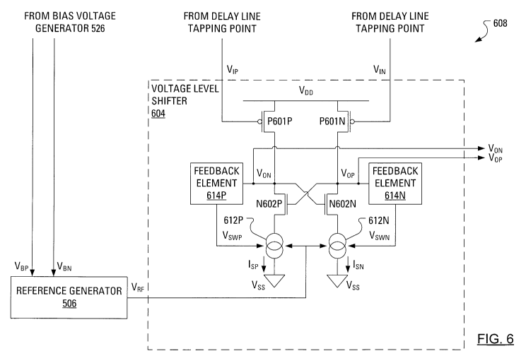
[0042] A buffer 608 is illustrated in FIG. 6 as including a non-specific
voltage level
shifter 604. The buffer 608 of FIG. 6 is generally consistent with the buffer
508 of FIG. 5,
however, the buffer 608 of FIG. 6 omits structures consistent with the input
buffers 510P,
510N. The non-specific voltage level shifter 604 has a first input PMOS
transistor P601P
and a second input PMOS transistor P601N. The non-specific voltage level
shifter 604 also
has a load chain, which load chain comprises a pair of transistors that have
an opposite
polarity to the input transistors. The load chain transistors include a first
NMOS load chain
transistor N602P and a second NMOS load chain transistor N602N. The drain of
the first
NMOS load chain transistor N602P is connected to the drain of the first PMOS
transistor
P601P, the gate of the second NMOS load chain transistor N602N and a the input
of a first
feedback element 614P. The drain of the second NMOS load chain transistor
N602N is
connected to the drain of the second PMOS transistor P601N, the gate of the
first NMOS
load chain transistor N602P and the input of a second feedback element 614N.
That is, the
first NMOS load chain transistor N602P and the second NMOS load chain
transistor
N602N are cross-coupled.
[0043] The load chain also includes a first regulated current source 612P,
which is
connected between the source of the first NMOS load chain transistor N602P and
a supply
voltage Vss, and a second regulated current source 612N, which is connected
between the
source of the second NMOS load chain transistor N602N and the supply voltage
Vss. The
current of the first regulated current source 612P is controlled by the
reference voltage VRF
received at a reference voltage terminal and by a first feedback signal, Vswp.
The reference
11
CA 02686701 2009-10-27
WO 2008/131545 PCT/CA2008/000794
voltage VRF is produced by the reference generator 506. The first feedback
signal Vswp is
produced by the first feedback element 614P. The current of the second
regulated current
source 612N is controlled by the reference voltage VRF and by a second
feedback signal,
VswN, produced by the second feedback element 614N.
[0044] In overview, the non-specific voltage level shifter 604 has the pair of
input
PMOS transistors P601P, P601N and a pair of load chains, each including one of
the cross-
coupled NMOS load chain transistors N602P, N602N and one of the regulated
current
sources 612P, 612N. The currents of the regulated current sources 612P, 612N
may be
controlled, in part, by the reference voltage VRF, produced by the reference
generator 506,
the first feedback signal Vswp, produced by the first feedback element 614P,
and the second
feedback signal VswN, produced by the second feedback element 614N.
[0045] The reference generator 506 produces the reference voltage VRF that is
used by
the regulated current sources 612P, 612N so that currents in the load chains
are maintained
proportional to maximum currents produced by the input PMOS transistors P601P,
P601N
and responsive to the change of the maximum currents caused by change of the
input signal
voltage swing, U. The reference generator 506 may, when producing the
reference voltage
VRF, use bias voltages VBN and VBP, which are produced by the bias voltage
generator 526
and are correlated to the swing U, on which depends the maximum current
produced by the
input PMOS transistors P601P, P601N.
[0046] The extremes of the voltage swing in the example delay line signal are
the
supply voltage VDD and a voltage close to the bias voltage VBP. As the value
of the bias
voltage VBP changes (to provide a variable delay in the delay line), the lower
level of the
voltage swing U also changes. The change in the lower level of the voltage
swing U, in turn,
causes a change in the maximum current that the input PMOS transistors P601P,
P601N can
produce. At the lower level of the voltage swing U, the gate voltage for a
given one of the
input PMOS transistors P601P, P601N is the bias voltage VBP. It follows then,
that, at the
lower level of the voltage swing U, the gate-source voltage for the given one
of the input
PMOS transistors P601P, P601N is equal to VDD-VBp and is relatively lower.
[0047] While the cross-coupled NMOS load chain transistors N602P, N602N
beneficially reduce DC current consumption in the non-specific voltage level
shifter 604,
the cross-coupled NMOS load chain transistors N602P, N602N also introduce some
12
CA 02686701 2009-10-27
WO 2008/131545 PCT/CA2008/000794
hysteresis, that is, a delay in switching the voltage on output terminals VON
and VoP
responsive to a switch occurring on the differential input terminals Vip and
VfN.
[0048] It should be understood that if the maximum current of the input PMOS
transistors P601P, P601N is less than the current in the cross-coupled NMOS
load chain
transistors N602P, N602N, the switching will not happen. A given one of the
NMOS load
chain transistors N602P, N602N will simply be unable to overpull the load
chain and flip
the output. For this reason, the strength of the load chain devices is
restricted through the
use of the regulated current sources 612P, 612N. The strength of the regulated
current
sources 612P, 612N is, in turn, coordinated with the strength of the input
PMOS transistors
P601P, P601N. An optimized coordination (a properly designed reference
generator 506)
will minimize the influence of hysteresis, meaning the load chain will
appropriately flip the
value on the output terminal in all conditions and delay caused by hysteresis
will be
minimized.
[0049] In operation, the voltage level shifter 504 transforms a differential
limited-
swing (e.g., from the supply voltage VDD to the bias voltage VBp) AC signal,
which is
received at the differential input terminals VlP and VIN connected to tapping
points in the
example delay line, into a differential full-swing (e.g., from the supply
voltage VDD to the
supply voltage Vss) AC signal at output terminals, identified as VON and Vop.
For the sake
of simplicity, it is assumed that the self-biased system comprising the delay
elements 502
and the bias voltage generator 526 operates so that an AC signal in the delay
line (at the
tapping points) is characterized by a voltage swing U from the supply voltage
VDD down to
a voltage level very close to the bias voltage VBP.
[0050] When the input terminal VIN is at the lower level (close to the bias
voltage VBP,
in the current example) and the input terminal VjP is at the higher level (the
supply voltage
VDD, the current example), the output terminal Vop is at the supply voltage
VDD and the
output terminal VON is at the supply voltage Vss. In particular, since the
gate (VIN) of the
second input PMOS transistor P601N is at a low voltage, the second input PMOS
transistor
P601N is ON. In contrast, since the gate (VlP) of the first input PMOS
transistor P601P is at
a high voltage, the second input PMOS transistor P601N is OFF. Since the gate
of the first
NMOS load chain transistor N602P is directly connected to the output terminal
VoP and the
output terminal Vop is at a high voltage, the first NMOS load chain transistor
N602P is ON
13
CA 02686701 2009-10-27
WO 2008/131545 PCT/CA2008/000794
and the voltage at the output terminal VON is allowed to take on a value close
to the supply
voltage Vss. In contrast, since the gate of the second NMOS load chain
transistor N602N is
at a low voltage (VON = Vss), the second NMOS load chain transistor N602N is
OFF.
[0051] The output terminal VON is held down to the supply voltage Vss by the
drive of
the load chain including the first NMOS load chain transistor N602P and the
first regulated
current source 612P. After a transition on the output terminal VON is
finished, a small
amount of current will suffice to hold the voltage on the output terminal VON
down.
Accordingly, the current in the first NMOS load chain transistor N602P and the
first
regulated current source 612P can be reduced. This reduction, in turn, can be
shown to help
to make the rising voltage transition on the output terminal VON faster, since
the first input
PMOS transistor P601P now has less of the drive of the load chain to over-
pull.
[0052] When the input terminal Vlp is at the lower level (close to the bias
voltage VBP,
in this example) and the input terminal VIN is at the higher level (the supply
voltage VDD, in
this example), the output terminal VON is at the supply voltage VDD and the
output terminal
Vop is at the supply voltage Vss=
[0053] In particular, since the gate (Vip) of the first input PMOS transistor
P601P is at a
lower level, the first input PMOS transistor P601P is ON. In contrast, since
the gate (VIN) of
the second input PMOS transistor P601N is at a high voltage, the second input
PMOS
transistor P601N is OFF. Since the gate of the second NMOS load chain
transistor N602N
is directly connected to the output terminal VON and the output terminal VON
is at a high
voltage, the second NMOS load chain transistor N602N is ON and the voltage at
the output
terminal Vop is allowed to take on a value close to the supply voltage Vss. In
contrast, since
the gate of the first NMOS load chain transistor N602P is at a low voltage
(Vop = Vss), the
first NMOS load chain transistor N602P is OFF.
[0054] The output terminal Vop is held down to the supply voltage Vss by the
drive of
the load chain including the second NMOS load chain transistor N602N and the
second
regulated current source 612N. After a transition on output terminal VoP is
finished, a small
amount of current will suffice to hold the voltage on the output terminal VoP
down.
Accordingly, the current in the second NMOS load chain transistor N602N and
the second
regulated current source 612N can be reduced. This reduction, in turn, can be
shown to help
14
CA 02686701 2009-10-27
WO 2008/131545 PCT/CA2008/000794
to make the rising voltage transition on the output terminal Vop faster, since
the second
input PMOS transistor P601N now has less of the drive of the load chain to
over-pull.
[0055] The first feedback element 614P produces a first feedback signal, VswP,
indicative of the state of the output terminal VoN. Consequently, as the state
of the output
terminal VON changes, the value of the current through the first regulated
current source
612P, Isp, changes. The first feedback element 614P is characterized by a
predetermined
delay between the time when the state of VON changes and the time when the
value of the
first feedback signal Vswp changes. The second feedback element 614N produces
a second
feedback signal, VSWN, indicative of the state of the output terminal VoP.
Consequently, as
the state of the output terminal VoP changes, the value of the current through
the second
regulated current source 612N, ISN, changes. The second feedback element 614N
is
characterized by a predetermined delay between time when the state of VoP
changes and the
time when the value of the second feedback signal VSWN changes.
[0056] The current, Isp, produced in the first regulated current source 612P
may be
arranged to have two components. A first component, a nominal value, is
determined by the
voltage level of the reference voltage VRF output from the reference generator
506. A
second component is determined by the voltage level of the first feedback
signal VswP
output from the first feedback element 614P. In a similar manner, the current,
ISN, produced
in the second regulated current source 612N may also be arranged to have two
components.
A first component, a nominal value, is determined by the voltage level of the
reference
voltage, VRF, output from the reference generator 506. A second component is
determined
by the voltage level of the second feedback signal VSWN output from the second
feedback
element 614N. As the value of the first feedback signal Vswp and the value of
the second
feedback signal VSwN change, the second component of the corresponding current
Isp and
ISN also changes. The contributions, to the overall Isp and ISN currents, of
the second current
components are smaller than the contributions of the first current components.
[0057] Alternatively, both the first components and the second components of
the
currents Isp and IsN may depend on the reference voltage value VRF and, then,
the entirety of
each current is divided into the two parts (components). In such a scenario,
the first part
(always present in the IsN current and the IsP current) is a fixed portion of
the overall IsN and
CA 02686701 2009-10-27
WO 2008/131545 PCT/CA2008/000794
Isp current and the second part (switched on or off according to the states of
the Vop and
VON outputs) is the remaining portion of the overall IsN and Isp current.
[0058] A person of ordinary skill in the art will appreciate that the first
input buffer
510P and the second input buffer 510N are optional. Furthermore, it should be
clear that the
input buffers 510P, 510N could be replaced with other circuits, such as
amplifiers or
repeaters.
[0059] The first input buffer 510P and the second input buffer 510N (or
amplifiers or
repeaters), when used, may provide an increased voltage swing or may move both
the
higher extreme and the lower extreme of the swing by a voltage difference. In
the example
arrangement of FIG. 6, the higher extreme may be less than the supply voltage
VDD by VT,
where VT is the threshold voltage of the input PMOS transistors P601P, P601N.
Similarly,
the lower extreme may be less than the bias voltage VBP by VT. Where VT is the
threshold
voltage of the input PMOS transistors P601P, P601N. Notably, in general VT can
be many
other kinds of voltage differences, for example, VT can be an NMOS threshold
or a
threshold difference or a compensated/stabilized voltage difference, dependent
upon on
complexity of the first input buffer 510P and the second input buffer 510N.
[0060] Such a reduction of the swing extremes causes the input PMOS
transistors
P601P, P601N to be closer to their ON state (with their gate-source voltages
close to VT)
when the input terminals VIp and VIN are at their higher extremes and have VT
more of gate-
source voltage when the input terminals ViP and VIN are at their lower
extremes. This closer
proximity to the ON state effectively increases the drive of the input PMOS
transistors
P601P, P601N and can be shown to shorten the AC signal propagation delay
through the
non-specific voltage level shifter 604.
[00611 As an aside, the bias voltage generator 526 can also produce a
reference signal
indicative of the maximum currents at the differential input terminals VlP and
VIN, for
instance, by mimicking a portion of the delay line with one input permanently
wired to one
state, effectively taking a function of the bias voltage generator 526.
[0062] A first possible implementation 704 of the non-specific voltage level
shifter 604
of FIG. 6 in combination with a first possible implementation 706 of the
reference generator
506 of FIGS. 5 and 6 are illustrated together in FIG. 7 as forming a buffer
708. Notably
16
CA 02686701 2009-10-27
WO 2008/131545 PCT/CA2008/000794
absent from the first voltage level shifter implementation 704 are
implementations of the
feedback elements 614P, 614N. A person of ordinary skill will appreciate that
such
feedback elements are not always necessary for the voltage level shifter 504
to achieve the
goal of transforming a differential limited-swing AC signal into a
differential full-swing AC
signal.
[0063] The first voltage level shifter implementation 704 includes the input
PMOS
transistors P601P, P601N and the pair of opposite-polarity, cross-coupled,
NMOS load
chain transistors N602P, N602N familiar from the non-specific voltage level
shifter 604 of
FIG. 6. As in the non-specific voltage level shifter 604 of FIG. 6, the input
terminal ViP
connects to the gate of first input PMOS transistor P601 P and the input
terminal VIN
connects to the gate of the second input PMOS transistor P601N. The first
regulated current
source 612P is implemented as a first current source NMOS transistor N701 P
and the
second regulated current source 612N is implemented as a second current source
NMOS
transistor N701N. In particular, the drain of the first current source NMOS
transistor N701P
is connected to the source of the first NMOS load chain transistor N602P and
the source of
the first current source NMOS transistor N701P is connected to the supply
voltage Vss=
Furthermore, the drain of the second current source NMOS transistor N701N is
connected
to the source of the second NMOS load chain transistor N602N and the source of
the second
current source NMOS transistor N701N is connected to the supply voltage Vss.
[0064] The first reference generator implementation 706 connects to a
reference source
to receive the bias voltage VBP and includes a first bias generation PMOS
transistor P701, a
first bias generation NMOS transistor N701 and a second bias generation NMOS
transistor
N702. In particular, the source of the first bias generation PMOS transistor
P701 is
connected to the supply voltage VDD, the drain of the first bias generation
PMOS transistor
P701 is connected to the drain of the second bias generation NMOS transistor
N702 and the
gate of the first bias generation PMOS transistor P701 is connected to the
input to the first
reference generator implementation 706 that receives the bias voltage VBP. The
gate of the
second bias generation NMOS transistor N702 is connected to the supply voltage
VDD and
the source of the second bias generation NMOS transistor N702 is connected to
the drain of
the first bias generation NMOS transistor N701. The gate of the first bias
generation NMOS
transistor N701 is connected to the drain of the first bias generation NMOS
transistor N701
and also acts as the reference voltage VRF output from the first reference
generator
17
CA 02686701 2009-10-27
WO 2008/131545 PCT/CA2008/000794
implementation 706. The source of the first bias generation NMOS transistor
N701 is
connected to the supply voltage Vss.
[0065] The reference voltage VRF output from the first reference generator
implementation 706 is received at the reference voltage terminal and
subsequently at the
gate of the first current source NMOS transistor N701 P and at the gate of the
second current
source NMOS transistor N701N.
[0066] In operation, the first bias generation PMOS transistor P701, being
similar to
the input PMOS transistors P601P, P601N of the first voltage level shifter
implementation
704, produces a current proportional to the maximum current that the input
PMOS
transistors P601P, P601N can produce when their gates, which are connected to
the
differential input terminals Vip and VIN, are at the lower level of the
voltage swing U. In this
example, the lower level of the voltage swing U is close to the bias voltage
VBP and the first
bias generation PMOS transistor P701 receives the bias voltage VBp at its
gate.
[0067] A reference current, IREF, flows through a bias generation chain
comprising the
first bias generation NMOS transistor N701 and the second bias generation NMOS
transistor N702. The bias generation chain mimics the load chains formed as a
combination
of the first NMOS load chain transistor N602P and the first current source
NMOS transistor
N701P in one case and formed as a combination of the second NMOS load chain
transistor
N602N and the second current source NMOS transistor N701N in the other case.
The gate
of the second bias generation NMOS transistor N702 is connected to the supply
voltage
VDD, which voltage level is representative of the highest level of voltage
attainable by the
gate of the first NMOS load chain transistor N602P and the gate of the second
NMOS load
chain transistor N602N.
[0068] As illustrated in FIG. 7, a pull-down current Ip flows through the
first NMOS
load chain transistor N602P and the first current source NMOS transistor N701
P.
Additionally, a pull-down current IN flows through the second current source
NMOS
transistor N701N and the second NMOS load chain transistor N602N. When the
pull-down
current Ip is flowing in the first load chain of the first voltage level
shifter implementation
704, the relationship to the reference current, IREF, flowing through the bias
generation chain
in the first reference generator implementation 706 is given by IP = m * IREF,
where the
value of "m" is determined from a ratio of the size of the first bias
generation NMOS
18
CA 02686701 2009-10-27
WO 2008/131545 PCT/CA2008/000794
transistor N701 to the size of the first current source NMOS transistor N701
P. When the
pull-down current IN is flowing in the second load chain of the first voltage
level shifter
implementation 704, the relationship to the reference current, IREF, flowing
through the bias
generation chain in the first reference generator implementation 706 is given
by IN = m*
IREF, where the value of "m" is determined from a ratio of the size of the
first bias
generation NMOS transistor N701 to the size of the second current source NMOS
transistor
N701N. Notably, the first current source NMOS transistor N701P and the second
current
source NMOS transistor N701N should be very similar, if not identical.
Accordingly, the
value of "m" should be the same for both current source NMOS transistors
N701P, N701N.
[0069] Conveniently, the pull-down currents (i.e., IP or IN) of the load
chains are
expected to track the peak current capability of the input PMOS transistors
P601P, P601N,
which peak current capability, in turn, is expected to vary as the swing U
varies.
[0070] A second possible implementation 804 of the non-specific voltage level
shifter
604 of FIG. 6 in combination with a second possible implementation 806 of the
reference
generator 506 are illustrated together in FIG. 8 as making up a buffer 808.
The second
voltage level shifter implementation 804 of FIG. 8 includes the input PMOS
transistors
P601P, P601N and the pair of opposite-polarity, cross-coupled, NMOS load chain
transistors N602P, N602N familiar from the non-specific voltage level shifter
604 of FIG. 6.
As in the non-specific voltage level shifter 604 of FIG. 6, the input terminal
VIp connects to
the gate of first input PMOS transistor P601P and the input terminal VIN
connects to the
gate of the second input PMOS transistor P601N.
[0071] The first regulated current source 612P is interposed between the first
NMOS
load chain transistor N602P and the supply voltage Vss and is implemented in
two paths: a
path Pl; and a path P2. A pull-down current IPi flows in path P1 and a pull-
down current IPZ
flows in path P2. In the path P1, the drain of a first path PI NMOS transistor
N801P1 is
connected to the source of the first NMOS load chain transistor N602P and the
drain of a
second path P 1 NMOS transistor N803P 1 is connected to the source of the
first path P 1
NMOS transistor N801P1. The source of the second path Pl NMOS transistor
N803P1 is
connected to the supply voltage Vss. In the path P2, the drain of a first path
P2 NMOS
transistor N801P2 is connected to the source of the first NMOS load chain
transistor N602P
and the drain of a second path P2 NMOS transistor N803P2 is connected to the
source of
19
CA 02686701 2009-10-27
WO 2008/131545 PCT/CA2008/000794
the first path P2 NMOS transistor N801 P2. The source of the second path P2
NMOS
transistor N803P2 is connected to the supply voltage Vss and the gate of the
second path P2
NMOS transistor N803P2 is connected to the supply voltage VDD.
[0072] The second regulated current source 612N is interposed between the
second
NMOS load chain transistor N602N and the supply voltage Vss and is also
implemented in
two paths: a path N 1; and a path N2. A pull-down current IN I flows in path N
1 and a pull-
down current IN2 flows in path N2. In the path N1, the drain of a first path
N1 NMOS
transistor N801N1 is connected to the source of the second NMOS load chain
transistor
N602N and the drain of a second path Nl NMOS transistor N803N1 is connected to
the
source of the first path Nl NMOS transistor N801N1. The source of the second
path N1
NMOS transistor N803N1 is connected to the supply voltage Vss. In the path N2,
the drain
of a first path N2 NMOS transistor N801N2 is connected to the source of the
second NMOS
load chain transistor N602N and the drain of a second path N2 NMOS transistor
N803N2 is
connected to the source of the first path N2 NMOS transistor N801N2. The
source of the
second path N2 NMOS transistor N803N2 is connected to the supply voltage Vss
and the
gate of the second path N2 NMOS transistor N803N2 is connected to the supply
voltage
UDD=
[0073] The second reference generator implementation 806 connects to a
reference
source to receive the bias voltage VBp and includes a first bias generation
PMOS transistor
P801, a first bias generation NMOS transistor N801, a second bias generation
NMOS
transistor N802 and a third bias generation NMOS transistor N803. In
particular, the source
of the first bias generation PMOS transistor P801 is connected to the supply
voltage VDD,
the drain of the first bias generation PMOS transistor P801 is connected to
the drain of the
second bias generation NMOS transistor N802 and the gate of the first bias
generation
PMOS transistor P801 is connected to the input to the second reference
generator
implementation 806 that receives the bias voltage VBP. The gate of the second
bias
generation NMOS transistor N802 is connected to the supply voltage VDD and the
source of
the second bias generation NMOS transistor N802 is connected to the drain of
the first bias
generation NMOS transistor N801. The gate of the first bias generation NMOS
transistor
N801 is connected to the drain of the first bias generation NMOS transistor
N801 and also
acts as the reference voltage VRF output from the second reference generator
implementation 806. The source of the first bias generation NMOS transistor
N801 is
CA 02686701 2009-10-27
WO 2008/131545 PCT/CA2008/000794
connected to the drain of the third bias generation NMOS transistor N803. The
gate of the
third bias generation NMOS transistor N803 is connected to the supply voltage
VDD and the
source of the third bias generation NMOS transistor N803 is connected to the
supply
voltage Vss.
[0074] The reference voltage VRF output from the second reference generator
implementation 806 is received at the reference voltage terminal and then,
from left to right,
the gate of the first path Pl NMOS transistor N801P1, the gate of the first
path P2 NMOS
transistor N801P2, the gate of the first path N2 NMOS transistor N801N2 and
the gate of
the first path NI NMOS transistor N801N1.
[0075] In contrast to the first voltage level shifter implementation 704 of
FIG. 7, the
second voltage level shifter implementation 804 of FIG. 8 includes
implementations of the
feedback elements 614P, 614N, which were presented in FIG. 6. In particular,
the first
feedback element 614P is implemented as a first digital buffer 814P and the
second
feedback element 614N is implemented as a second digital buffer 814N. As will
be clear to
a person of ordinary skill, digital buffers are most commonly made of an even
number of
serially connected inverters, but may also take the form of a First-In-First-
Out (FIFO)
memory.
[0076] The input to the first digital buffer 814P is received at the output
terminal VON
and the output of the first digital buffer 814P is connected to the gate of
the second path P 1
NMOS transistor N803P1. The input to the second digital buffer 814N is
received at the
output terminal Vop and the output of the second digital buffer 814N is
connected to the
gate of the second path N1 NMOS transistor N803N1.
[0077] In the operation of the second voltage level shifter implementation 804
of FIG.
8, the load chain current sources are regulated both by the second reference
generator
implementation 806 and by the digital buffers 814P, 814N. In a manner similar
to the first
reference generator implementation 706, the second reference generator
implementation
806 reproduces and monitors the maximum current of the input PMOS transistors
P601P,
P601N. The third bias generation NMOS transistor N803 compensates for the
resistance of
the bottom transistors in the various paths of the dual-path regulated current
sources,
namely the second path P1 NMOS transistor N803P1 and the second path N1 NMOS
transistor N803N1, as well as the second path N2 NMOS transistor N803N2 and
the second
21
CA 02686701 2009-10-27
WO 2008/131545 PCT/CA2008/000794
path P2 NMOS transistor N803P2. In particular, the third bias generation NMOS
transistor
N803 allows the chain that includes the second bias generation NMOS transistor
N802, the
first bias generation NMOS transistor N801 and the third bias generation NMOS
transistor
N803 to appropriately mimic, for the purpose of current mirroring, the
operation of the
chain that includes, for example, the first NMOS load chain transistor N602P,
the first path
P2 NMOS transistor N801P2 and the second path P2 NMOS transistor N803P2.
[0078] A reference current, IREF, flows through a bias generation chain
comprising the
second bias generation NMOS transistor N802, the first bias generation NMOS
transistor
N801 and the third bias generation NMOS transistor N803. The bias generation
chain
mimics the load chains in the second voltage level shifter implementation 804.
The gate of
the second bias generation NMOS transistor N802 is connected to the supply
voltage VDD,
which voltage level is representative of the highest level of voltage
attainable by the gate of
the first NMOS load chain transistor N602P and the gate of the second NMOS
load chain
transistor N602N.
[0079] The NMOS load chain devices in the second voltage level shifter
implementation 804, the first bias generation NMOS transistor N801 and the
third bias
generation NMOS transistor N803 together form a current mirror. Conveniently,
the current
mirror establishes a relationship between the reference current IREF and the
load chain
currents IPi, IP2, IN], IN2. All four load chain currents IP], IP2, INI, IN2
are fractions of the
reference current IREF, which, in turn, is proportional to the maximum current
of the input
PMOS transistors P601P, P601N reproduced by the first bias generation PMOS
transistor
P801 in the reference generator 806. The first bias generation PMOS transistor
P801 in the
reference generator 806 may be similar in size to the input PMOS transistors
P601P, P601N
of the buffer 808, in which case they produce a current IREF close to the
actual maximum
currents of the input PMOS transistors P601P, P601N. If the first bias
generation PMOS
transistor P801 is different in size from the input PMOS transistors P601P,
P601N, the
current IREF is a scaled replica of the maximum current of the input PMOS
transistors
P601P, P601N. This scaling factor will, in turn, reflect on the size ratio of
the current mirror
(ratio of the sizes of the third bias generation NMOS transistor N803 to the
sizes of the
bottom transistors in the various paths of the dual-path regulated current
sources
N803P1/N803P2/N803N1/N803N2 and ratio of the sizes of the first bias
generation NMOS
22
CA 02686701 2009-10-27
WO 2008/131545 PCT/CA2008/000794
transistor N801 to the sizes of the top transistors in the various paths of
the dual-path
regulated current sources N801P1/N801P2/N801N1/N801N2.
[0080] In particular, one of the ways to describe the ratios may be following:
IP] = IN1 = a * IREF and IPZ = IN2 = b * IREF. The coefficients a and b are
set by the size ratios.
In other words, the value of a is related to a ratio of the sizes of the
second path N1 NMOS
transistor N803N1 and the second path Pl NMOS transistor N803P1 to the size of
the third
bias generation NMOS transistor N803. The value of a is also related to a
ratio of the sizes
of the first path NI NMOS transistor N801N1 and the first path P1 NMOS
transistor
N801 P 1 to the size of the first bias generation NMOS transistor N801. For
another instance,
the value of b is related to a ratio of the sizes of the second path P2 NMOS
transistor
N803P2 and the second path N2 NMOS transistor N803N2 to the size of the third
bias
generation NMOS transistor N803. The value of b is also related to a ratio of
the sizes of the
first path N2 NMOS transistor N801N2 and the first path P2 NMOS transistor
N801P2 to
the size of the first bias generation NMOS transistor N801.
[0081] There are four current sources in FIG. 8: the first current source
consists of the
first path P 1 NMOS transistor N801 P 1 and the second path P 1 NMOS
transistor N803P 1;
and the second current source consists of the first path P2 NMOS transistor
N801P2 and
the second path P2 NMOS transistor N803P2. The first and second current
sources together
make a combined current source with a variable current value. The combined
current source
corresponds to the first regulated current source 612P of FIG. 6. The third
current source
consists of the first path NI NMOS transistor N801N1 and the second path N1
NMOS
transistor N803N1. The fourth current source consists of the first path N2
NMOS transistor
N801N2 and the second path N2 NMOS transistor N803N2. The third and fourth
current
sources together make a combined current source that corresponds to the second
regulated
current source 612N of FIG. 6.
[0082] Typically, in order to balance transition rates at the output nodes Vop
and VON,
it is chosen that Ipl = IN, and IP2 = IN2. It is anticipated that the ratio of
the value of the
reference current IREF to the total current (IPi+IPZ) in path PI and path P2
will be a constant,
"k". Furthermore, it is anticipated that the ratio of the value of the
reference current IREF to
the total current (INI +IN2) in path N1 and path N2 will be equivalent to the
same constant,
"k". The value of "k" is determined by a ratio of the size of the first bias
generation NMOS
23
CA 02686701 2009-10-27
WO 2008/131545 PCT/CA2008/000794
transistor N801 to the size of the first path P 1 NMOS transistor N801 P 1 and
the size of the
first path P2 NMOS transistor N801P2. The value of "k" will also be determined
by a ratio
of the size of the first bias generation NMOS transistor N801 to the size of
the first path N1
NMOS transistor N801N1 and the size of the first path N2 NMOS transistor
N801N2.
Notably, the first path Pl NMOS transistor N801P1, the first path P2 NMOS
transistor
N801P2, the first path N1 NMOS transistor N801N1 and the first path N2 NMOS
transistor
N801N2 should be structurally very similar, if not identical. Value of the
coefficient "k"
might be determined, alternatively or in part, by the ratio of the sizes of
the first bias
generation PMOS transistor P801 to sizes of the input PMOS transistors P601P,
P601N.
[0083] In review, in path P2, the gate of the second path P2 NMOS transistor
N803P2
is connected to the supply voltage VDD, thereby permanently enabling the
current IP2 in path
P2. Furthermore, in path N2, the gate of the second path N2 NMOS transistor
N803N2 is
connected to the supply voltage VDD, thereby permanently enabling the current
IN2 in path
N2.
[0084] The first digital buffer 814P delays signal propagation from node VON
to the
gate of the second path P1 NMOS transistor N803P 1. The second digital buffer
814N
delays signal propagation from the node Vop to the gate of the second path Nl
NMOS
transistor N803N1.
[0085] The first digital buffer 814P and the second digital buffer 814N are
characterized by a predetermined delay of signal propagation from their inputs
to their
outputs.
[0086] A first feedback signal at the output of the first digital buffer 814P,
which first
feedback signal is identified in FIG. 8 as Vswp, controls the amount of
current flowing in
the path P1 based on the voltage level at the output terminal VON. In
particular, at a time x
seconds, where x seconds is the predetermined delay, after the voltage at the
output terminal
VON has gone high, the first feedback signal Vswp goes high and turns on the
second path P 1
NMOS transistor N803P 1, thereby enabling the current in the path P1. At a
time x seconds
after the voltage at the output terminal VON has gone low, the first feedback
signal Vswp
goes low and turns off the second path P1 NMOS transistor N803P1, thereby
disabling the
current in the path P 1.
24
CA 02686701 2009-10-27
WO 2008/131545 PCT/CA2008/000794
[0087] Conveniently, the allowance, by the second path P 1 NMOS transistor
N803P 1,
of the flow of current in the path P 1 becomes important when the voltage at
the output
terminal VON goes through a transition from high to low. The two-path load
chains of the
second voltage level shifter implementation 804 allow the speed of the
transition from high
to low to be increased, relative to the transitions speed available using the
single-path load
chains of the first voltage level shifter implementation 704.
[0088] Much in the same way that the first digital buffer 814P controls the
flow of
current in the path P 1 based on a delayed version of the voltage at output
terminal VON, the
second digital buffer 814N controls the flow of current in the path N1 based
on a delayed
version of the voltage at output terminal VoP.
[0089] In an alternative implementation for the second voltage level shifter
implementation 804 of FIG. 8, input of the second digital buffer 814N is
connected to the
output terminal VON, and the input of the first digital buffer 814P is
connected to the output
terminal Vop. In this case, the first digital buffer 814P and the second
digital buffer 814N
will be required to invert and will, for example, consist of an odd number of
serially
connected inverters.
[0090] FIG. 9 illustrates the first voltage level shifter implementation 704
in a buffer
908 with a third possible implementation 906 of the reference generator 506.
The buffer 908
also includes a first source follower 910P and a second source follower 910N
at the inputs
of the first voltage level shifter implementation 704.
[0091] The third reference generator implementation 906 connects to a
reference
source to receive the bias voltage VBP and includes a first bias generation
PMOS transistor
P901, a first bias generation NMOS transistor N901, a second bias generation
NMOS
transistor N902, a bias generation source follower transistor N90R and a bias
generation
current source 905. In particular, the drain of the bias generation source
follower transistor
N90R is connected to the supply voltage VDD, the source of the bias generation
source
follower transistor N90R is connected to the bias generation current source
905 and the gate
of the bias generation source follower transistor N90R is connected to the
input to the third
reference generator implementation 906 that receives the bias voltage VBP. The
source of
the first bias generation PMOS transistor P901 is connected to the supply
voltage VDD, the
drain of the first bias generation PMOS transistor P901 is connected to the
drain of the
CA 02686701 2009-10-27
WO 2008/131545 PCT/CA2008/000794
second bias generation NMOS transistor N902 and the gate of the first bias
generation
PMOS transistor P901 is connected to the source of the bias generation source
follower
transistor N90R. The gate of the second bias generation NMOS transistor N902
is
connected to the supply voltage VDD and the source of the second bias
generation NMOS
transistor N902 is connected to the drain of the first bias generation NMOS
transistor N901.
The gate of the first bias generation NMOS transistor N901 is connected to the
drain of the
first bias generation NMOS transistor N901 and also acts as the reference
voltage VRF
output from the third reference generator implementation 906. The source of
the first bias
generation NMOS transistor N901 is connected to the supply voltage Vss=
[0092] The reference voltage VRF output from the third reference generator
implementation 906 is received at the reference voltage terminal and then at
the gate of the
first current source NMOS transistor N701 P and at the gate of the second
current source
NMOS transistor N701N.
[0093] The first source follower 910P and the second source follower 910N are
presented as optional examples of the input buffers 510P, 510N illustrated in
FIG. 5 as
interposing the delay line and the voltage level shifter 504. In particular,
the first source
follower 910P includes a first source follower NMOS transistor N90RP and a
first current
source 905P. Similarly, the second source follower 910N includes a second
source follower
NMOS transistor N90RN and a second current source 905N.
[0094] The drain of the first source follower NMOS transistor N90RP is
connected to
the supply voltage VDD and the gate of the first source follower NMOS
transistor N90RP is
connected to an alternative input terminal ViPl. The first current source 905P
is connected
between the source of the first source follower NMOS transistor N90RP and the
supply
voltage Vss.
[0095] The drain of second first source follower NMOS transistor N90RN is
connected
to the supply voltage VDD and the gate of the second source follower NMOS
transistor
N90RN is connected to an alternative input terminal VINI. The second current
source 905N
is connected between the source of the second source follower NMOS transistor
N90RN
and the supply voltage Vss.
26
CA 02686701 2009-10-27
WO 2008/131545 PCT/CA2008/000794
[0096] The gate of the first input PMOS transistor P601 P connects to the
source of the
first source follower NMOS transistor N90RP.
[0097] The gate of the second input PMOS transistor P601N connects to the
source of
the second source follower NMOS transistor N90RN.
[0098] In keeping with the voltage level shifter 504 of FIG. 5, the input
terminal VlPI of
the first voltage level shifter implementation 704 is illustrated in FIG. 9 as
connecting to the
delay line tapping point though the first source follower 910P. As mentioned
hereinbefore,
the first source follower 910P is an example implementation of the first input
buffer 510P.
Similarly, by interposing the input terminal VoP and the delay line tapping
point, the second
source follower 910N is an example implementation of the second input buffer
510N. A
first source follower input terminal VIPl and a second source follower input
terminal VIN, are
connected to the tapping points.
[0099] It is expected that the voltage level shifter 504 may be used in high-
frequency
applications, wherein the slew rate at the output terminals VON and VoP needs
to be
increased. The slew rate at the output terminals VON and Vop is determined by
currents in
the input PMOS transistors P601P, P601N. One way to increase the current in
the input
PMOS transistors P601P, P601N is to increase the size of the input PMOS
transistors
P601P, P601N. However, as the size of the input PMOS transistors P601P, P601N
is
increased, the load at the tapping points of the delay chain is also
increased. By designing
the buffer 908 so that the source follower NMOS transistors N90RP, N90RN are
much
smaller than the input PMOS transistors P601P, P601N, the use of the source
followers
910P, 910N may be seen to reduce load at the tapping points of the delay
chain.
[0100] Another function of the source followers 910P, 910N is to bring down
voltage
levels of the voltage swing at the gates of the input PMOS transistors P601P,
P601N. The
first input PMOS transistor P601P conducts when the gate voltage drops below
VDD-VTP,
where VTP is the threshold voltage of the first input PMOS transistor P601 P.
Without the
source followers 910P, 910N, the voltage at the gate of the input PMOS
transistor P601P,
for example, swings between the supply voltage VDD and the bias voltage VBP.
That is, the
peak of the voltage swing at the gates of the first input PMOS transistor
P601P is the supply
voltage VDD. With the source followers 910P, 910N, the voltage at the gate of
the input
PMOS transistor P601P swings between VDD-VTN and VBP-VTN, where VTN is the
gate-to-
27
CA 02686701 2009-10-27
WO 2008/131545 PCT/CA2008/000794
source voltage of the first source follower NMOS transistor N90RP. That is,
the peak of the
voltage swing at the gates of the first input PMOS transistor P601P is VDD-
VTN. Since VDD-
VTN is closer to VDD-VTP than the supply voltage VDD is to VDD-VTP, the time
necessary for
the first input PMOS transistor P601P to start driving (conducting current) is
reduced. The
operation of the second input PMOS transistor P601N may be analyzed similarly.
[0101] The buffer 908 of FIG. 9 shows only one implementation of the source
followers 910P, 910N, the operation of which depends, for example, on both the
threshold
voltage VTP of the input PMOS transistors P601P, P601N and the gate-to-source
voltage
VTN of the first source follower NMOS transistor N90RP. Unfortunately, the
PMOS
threshold voltage, VTP, and the NMOS gate-to-source voltage, VTN, have
different
dependences on operation conditions (e.g., temperature) and process parameters
variations.
One of ordinary skill in the art will understand that further implementations
of the source
followers 910P, 910N can be built so that better voltage compensation can be
achieved.
[0102] A voltage level shifter built in accordance with example embodiments
may be
adjusted to handle various combinations of power supply voltage level (the
supply voltage
VDD in all the examples above) and input voltage swing. For instance, in order
to
accommodate a particular voltage combination, schemes can be "VDD-VSS
mirrored". That
is, NMOS devices used in place of PMOS devices and PMOS devices used in place
of
NMOS devices, with necessary size adjustments. The skilled practitioner will
also recognize
that such transformations serve only to adapt different voltage conditions and
do not deviate
from main ideas of example embodiments.
[0103] FIG. 10 is presented as an illustrative example of VDD-VSS mirroring.
In
particular, a buffer 1008 in FIG. 10 is representative of the buffer 708 of
FIG. 7 wherein
NMOS devices have been used in place of PMOS devices and PMOS devices have
been
used in place of NMOS devices, with necessary size adjustments.
[0104] A third possible implementation 1004 of the non-specific voltage level
shifter
604 of FIG. 6 in combination with a fourth possible implementation 1006 of the
reference
generator 506 of FIGS. 5 and 6 are illustrated together in FIG. 10 as forming
the buffer
1008. Absent from the third voltage level shifter implementation 1004 are
implementations
of the feedback elements 614P, 614N.
28
CA 02686701 2009-10-27
WO 2008/131545 PCT/CA2008/000794
[0105] The third voltage level shifter implementation 1004 includes a first
input
NMOS transistor N1001P, a second input NMOS transistor N1001N, a first PMOS
load
chain transistor P 1002P and a second PMOS load chain transistor P 1002N. The
input
terminal VIp connects to the gate of the first input NMOS transistor N1001P
and the input
terminal VIN connects to the gate of the second input NMOS transistor N1001N.
The first
regulated current source 612P is implemented as a first current source PMOS
transistor
P 1001 P and the second regulated current source 612N is implemented as a
second current
source PMOS transistor P1001N. In particular, the drain of the first current
source PMOS
transistor P 1001 P is connected to the source of the first PMOS load chain
transistor P 1002P
and the source of the first current source PMOS transistor P 1001 P is
connected to the
supply voltage VDD. Furthermore, the drain of the second current source PMOS
transistor
P1001N is connected to the source of the second PMOS load chain transistor
P1002N and
the source of the second current source PMOS transistor P1001N is connected to
the supply
voltage VDD.
[0106] The fourth reference generator implementation 1006 connects to a
reference
source to receive the bias voltage VBP and includes a first bias generation
NMOS transistor
N1001, a first bias generation PMOS transistor P1001 and a second bias
generation PMOS
transistor P 1002. In particular, the source of the first bias generation NMOS
transistor
N1001 is connected to the supply voltage VSS, the drain of the first bias
generation NMOS
transistor N1001 is connected to the drain of the second bias generation PMOS
transistor
P 1002 and the gate of the first bias generation NMOS transistor N1001 is
connected to the
input to the fourth reference generator implementation 1006 that receives the
bias voltage
VBP. The gate of the second bias generation PMOS transistor P1002 is connected
to the
supply voltage Vss and the source of the second bias generation PMOS
transistor P1002 is
connected to the drain of the first bias generation PMOS transistor P1001. The
gate of the
first bias generation PMOS transistor P1001 is connected to the drain of the
first bias
generation PMOS transistor P1001 and also acts as the reference voltage VRF
output from
the fourth reference generator implementation 1006. The source of the first
bias generation
PMOS transistor P 1001 is connected to the supply voltage VpD.
[0107] The reference voltage VRF output from the fourth reference generator
implementation 1006 is received at the reference voltage terminal and
subsequently at the
29
CA 02686701 2009-10-27
WO 2008/131545 PCT/CA2008/000794
gate of the first current source PMOS transistor P 1001 P and at the gate of
the second
current source PMOS transistor P1001N.
[0108] In operation, the first bias generation NMOS transistor N1001, being
similar to
the input NMOS transistors P 1001 P, P 1001 N of the third voltage level
shifter
implementation 1004, produces a current proportional to the maximum current
that the input
NMOS transistors N 1001 P, N 1001 N can produce when their gates, which are
connected to
the differential input terminals Vlp and VIN, are at the lower level of the
voltage swing U.
[0109] A reference current, IREF, flows through a bias generation chain
comprising the
first bias generation PMOS transistor P1001 and the second bias generation
PMOS
transistor P1002. The bias generation chain mimics the load chains formed as a
combination
of the first PMOS load chain transistor P 1002P and the first current source
NMOS transistor
P1001P in one case and formed as a combination of the second PMOS load chain
transistor
P 1002N and the second current source PMOS transistor P 1001 N in the other
case. The gate
of the second bias generation PMOS transistor P 1002 is connected to the
supply voltage
Vss, which voltage level is representative of the lowest level of voltage
attainable by the
gate of the first PMOS load chain transistor P 1002P and the gate of the
second PMOS load
chain transistor P 1002N.
[0110] As illustrated in FIG. 10, a pull-down current Ip flows through the
first PMOS
load chain transistor P 1002P and the first current source PMOS transistor P
1001 P.
Additionally, a pull-down current IN flows through the second current source
PMOS
transistor P1001N and the second PMOS load chain transistor P1002N. When the
pull-
down current IP is flowing in the first load chain of the third voltage level
shifter
implementation 1004, the relationship to the reference current, IREF, flowing
through the
bias generation chain in the fourth reference generator implementation 1006 is
given by IP =
m * IREF, where the value of "m" is determined from a ratio of the size of the
first bias
generation PMOS transistor P 1001 to the size of the first current source PMOS
transistor
P 1001 P. When the pull-down current IN is flowing in the second load chain of
the third
voltage level shifter implementation 1004, the relationship to the reference
current, IREF,
flowing through the bias generation chain in the fourth reference generator
implementation
1006 is given by IN = m* IREF, where the value of "m" is determined from a
ratio of the size
of the first bias generation PMOS transistor P1001 to the size of the second
current source
CA 02686701 2009-10-27
WO 2008/131545 PCT/CA2008/000794
PMOS transistor P 1001 N. Notably, the first current source PMOS transistor P
1001 P and the
second current source NMOS transistor P1001N should be very similar, if not
identical.
Accordingly, the value of "m" should be the same for both current source NMOS
transistors
P 1001 P, P 1001 N.
[0111] Conveniently, the pull-down currents (i.e., IP or IN) of the load
chains are
expected to track the peak current capability of the input PMOS transistors
N1001P,
N1001N, which peak current capability, in turn, is expected to vary as the
swing U varies.
[0112] Conveniently, aspects of the proposed voltage level shifter may be
found to
result in a reduction of power consumption with limited or no DC current
thanks to a cross-
coupled transistor connection in the load chain. Generally, the load chain
consumes current
during an AC signal transition only and preferably does not have DC component
in current
consumption.
[0113] While the cross-coupling of the first NMOS load chain transistor N602P
and the
second NMOS load chain transistor N602N might be seen to introduce a
hysteresis effect.
The dynamically changing operation current values in the load chain controlled
by the
current sources help to mitigate the hysteresis effect. In this manner, the
current in the load
chain transistors N602P, N602N dynamically tracks the current in the input
PMOS
transistors P601P, P601N.
[0114] Further conveniently, the use of the source followers 910P, 910N may be
seen
to reduce load at the tapping points of the delay chain.
[0115] The above-described embodiments of the present application are intended
to be
examples only. Alterations, modifications and variations may be effected to
the particular
embodiments by those skilled in the art without departing from the scope of
the application,
which is defined by the claims appended hereto.
31