Note: Descriptions are shown in the official language in which they were submitted.
CA 02687307 2009-12-01
CONTROL ARRANGEMENT AND NIETHOD FOR ELECTRONIC DEVICE
BACKGROUND OF THE INVENTION
1. Field of the Invention
The present invention relates generally to the control of electronic devices
and more
particularly to a control arrangement and method that controls the conductive
state of an
electronic device such that the normal state is conductive and a predetermined
control signal is
required to render the power electronics device nonconductive.
2. Discussion of the related art
Various electronic systems are known where devices are controlled between
condtictive
and nonconductive states. In power electronic systems arranged as source-
transfer switches,
continuous power to a load is supplied by transferring the supply of the load
from one source to
another when undesirable characteristics are sensed in the source currently
supplying the load.
For example, the arrangement in U.S. Patent No. 5,808,378 provides desirable
control features
for the solid-state switches that are selectively rendered conductive to
supply current to a load
from one of two or more sources. Undesirable current flow between sources is
avoided and
transfer delays are minimized. In U.S. Patents 5,644,175 and 5,814,904, when a
transfer is
desired, current through the conducting solid-state switch is sensed twice
before signals are
removed from the conducting switch and applied to another solid-state switch
to provide current
through an alternate source. The arrangement in U.S. Patent No. 4,811,163
provides solid-state
switches across the main power contacts of automatic bus transfer equipment.
The solid-state
switch is rendered conductive before its respective main contact is closed and
a timer circuit
maintains the solid-state switch conductive for a predetermined time period
selected to ensure
that the main contact will be closed while the solid-state switch is still
conductive.
Since the controls for the power electronic devices utilized in these systems
are subject to
noise that may effect the conducting state of the switch by erroneously
turning it on or off. While
these arrangements may be useful and generally satisfactory for their intended
purposes, they are
prone to erroneously changing the conductive state of switches.
SUMMARY OF THE INVENTION
Accordingly it is a principal object of the present invention to provide a
control
arrangement for electronic devices in which an electronic switch is maintained
in a conducting
state at all times other than when it is desired to render the electronic
switch nonconducting.
CA 02687307 2009-12-01
It is another object to provide a control method and arrangement to control
the conducting
status of a power electronic switch via a latched control signal, such that
the appropriate receipt
of a secure, complex signal is required to change the conducting state of the
power electronic
switch.
It is a further object of the present invention to latch the conductive state
of a switch and
toggle the latch to render the switch nonconductive via the decoding of a
complex encoded
momentary signal.
It is yet another object of the present invention to provide a control that
maintains a
power electronic switch in a conducting state at all times other than when an
active signal is
received to tum off the power electronic switch.
These and other objects of the present invention are efficiently achieved by a
control
arrangement for electronic devices in which an electronic switch is maintained
in a conducting
state at all times other than when it is desired to render the electronic
switch nonconducting. In a
specific embodiment, a latched control signal is utilized which is changed by
the receipt of a
momentary signal to change the conducting state of the electronic switch. For
example,
according to one specific arrangement, the momentary signal is a secure,
complex signal such
that appropriate decoding and detection of the proper signal is required to
change the conducting
state of the electronic switch.
BRIEF DESCRIPTION OF THE DRAWING
The invention, both as to its organization and method of operation, together
with further
objects and advantages thereof, will best be understood by reference to the
specification taken in
conjunction with the accompanying drawing in which like references refer to
like elements and in
which:
FIGS. 1-4 are block diagram representations of four embodiments of four
respective
control arrangements of the present invention;
FIG. 5 is a block diagram representation of a high-speed source-transfer
switching system
utilizing the control arrangement of the present invention; and
FIG. 6 is a one-line, diagrammatic representation of portions of a solid-state
switch of
FIG. 5.
DETAILED DESCRIPTION
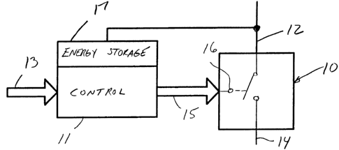
Referring now to FIG. 1, a control arrangement and method according to the
present
invention is utilized to control a power electronic device, e.g. an
illustrative electronic switch 10,
-2-
CA 02687307 2009-12-01
that includes a main path between lines 12 and 14 that is controlled between
on and off states,
corresponding to respective conductive and nonconductive states, via a control
connection at 16.
In specific examples, the electronic switch 10 is an SCR, thyristor, TRIAC,
IGBT, inverse-
parallel connected SCR's, or other actively controlled devices. A control
stage 11 provides
control signals at 15, e.g. "ON" and "OFF" state signals, to the control
connection 16 to control
the conductive state of the electronic switch 10. In a specific arrangement
the control 11 is
arranged to maintain the electronic switch 10 in the conductive state at all
times other than when
a control signal is generated at 15 to turn off the electronic switch 10, e.g.
the deliberate
generation by the control 11 of an active OFF signal at 15 is required to turn
off the electronic
switch 10. For example, with an AC waveform on line 12, the control 11 is
effective to
condition the electronic switch 10 to the conductive state each half cycle of
the AC waveform
when no OFF signal is generated. In a specific arrangement, the control 11 is
responsive to a
power-up input signal at 13 to continuously provide at all times thereafter an
ON signal to the
electronic switch 10 unless conditions are sensed that define a desired OFF
state signal be sent at
15 by the control 11 to turn off the electronic switch 10. In a specific
arrangement, an energy
storage stage 17 is provided that stores energy from the line 12 and provides
operating energy to
the control 11. Thus, the control 11 is capable of providing continuous
control to the electronic
switch 10 independent of the present, momentary state of the line 12, e.g. to
maintain the
electronic switch 10 in the conductive state.
In accordance with other aspects of the present invention and with reference
now to FIG.
2, an illustrative controller 18 provides control signals at 20 to a memory
stage 22. In a specific
arrangement, the control signals at 20 represent an "ON" or "OFF" command and
are generated
on a momentary basis, i.e. short duration, whenever it is desired to change
the conductive state of
the electronic switch 10. The memory stage 22 responds to the control signals
at 20 by providing
a latched output at 24 that changes output state only when a control signal at
20 is received which
represents a desired change in the conductive state of the electronic switch
10. The latched
output signal at 24 is provided to the control connection at 16 to control the
conductive state of
the electronic switch 10. Accordingly, when it is desired to change the
conductive state of the
electronic switch 10, the controller 18 issues a control signal at 20
whereupon the state of the
latched output signal at 24 is changed and the conductive state of the
electronic switch 10 is
changed. For example, in one specific arrangement, assuming that the
electronic switch 10 is
conducting and it is desired to tum off the electronic switch 10, a
predetermined OFF signal is
provided at 20. In response to the OFF signal at 20, the memory stage 22
changes the state of the
latched output signal at 24 to render the electronic switch 10 non-conducting.
In one specific
-3-
CA 02687307 2009-12-01
embodiment, the ON and OFF control signals at 20 are distinct predetermined
data words on a
data bus. In another specific arrangement, the control signals at 20 include a
separate control line
for each of the ON and OFF signals. In yet another specific arrangement, the
control signal at 20
is a momentary signal for a change of the conductive state which can be
characterized as toggling
the memory stage 22 whenever it is desired to change the conductive state of
the electronic
switch 10.
Considering now an illustrative embodiment of the control arrangement and
method of
the present invention for environments where the electronic switch 10 is
located remotely and
separated from the controller 18 and referring now to FIG. 3, the controller
18 provides an ON
signal at 19 and an OFF signal at 21 to an encoder stage 26. The encoder stage
26 encodes the
ON/OFF signals at 19, 21 and communicates over a communications link 28 to a
decoder
arrangement generally referred to at 30. The decoder arrangement 30 provides
latched output
signals at 25 to control the electronic switch 10. In response to the signals
at 19, 21, the encoder
stage 26 provides a predetermined ON or OFF encoded signal over the
communications link 28
to the decoder arrangement 30. The decoder arrangement 30 decodes the encoded
signal
received from the communications link 28 and changes the state of the latched
output signal at 25
in accordance with this decoded signal. For example, in a specific
arrangement, if the decoded
signal corresponds to an ON state, the signal at 25 is changed to or
maintained at the ON state to
the electronic switch 10. Correspondingly, if the decoded signal in the
decoder arrangement 25
corresponds to an OFF state, the signal at 25 is changed to or maintained at
the OFF state to the
electronic switch 10. In a specific arrangement, the ON and OFF signals at 19,
21 are momentary
pulse signals and the encoded signal is a pulse train including a
predetermined different number
of pulses for an OFF signal and an ON signal over the communications link 28.
The
communications link 28 in various implementations is provided by a dielectric
medium such as
fiber optics, infrared or various other communications media. The decoder
stage 30 determines
an ON or OFF signal based on the pulse count and appropriately changes the
latched output state
at 25 to correspond to the decoded signal at. In a specific illustrative
example as shown in FIG.
3, the decoder arrangement 30 includes a receiver/translator stage 32, a
memory stage 34 and a
driver stage 36. The receiver/translator stage 32 responds to the encoded
signals on the
communications link 28 and provides appropriate control to change the state of
the memory stage
34 via a signal path 33. The memory stage 34 provides a latched output at 35
to control the
driver stage 36. Such an arrangement is especially useful where the location
and environment of
the electronic switch 10 is a high noise environment such as where the
electronic switch 10
operates at medium voltages. In such embodiments, the communications link 28
is an isolating
-4-
CA 02687307 2009-12-01
link such as provided by fiber optics, infrared, pulse transformers etc. as
known in the art.
Additionally, in a preferred embodiment, the driver stage 36 includes
isolation between the input
at 35 and the output at 25 to the electronic switch 10. In a specific
implementation, the driver
stage 36 is arranged to provide gating signals to the electronic switch 10 at
25 each half cycle of
an AC waveform as long as the latching output at 35 corresponds to the ON
state.
Considering now another illustrative embodiment of the present invention and
referring
now additionally to FIG. 4, the illustrative electronic switch 10 is
implemented by a plurality of
series-connected electronic switch stages, e.g. as illustrated in FIG. 4 by
first and second stages
l0a and l Ob, and by a last stage l Ox. For each of the series-connected
electronic switch stages
10a to lOx, a respective decoder stage 30 is provided, e.g. as represented by
the respective
decoder stages 30a, 30b and 30x,. The decoder stages 30a to 30x receive
signals over respective
links 28a to 28x from the common encoder stage 26 and provide the respective
latched outputs
25a, 25b and 25x. In this manner, the electronic switch 10 with the plurality
of series-connected
stages is controlled by the controller 18 and the encoder stage 26. Where a
multi-phase power
electronic system is to be controlled, the electronic switch 10 provides one
pole of the system for
controlling conduction between the lines 12, 14 of one phase of the system. In
such an
arrangement, an additional encoder stage 26 is provided for each additional
phase, e.g. 26-2 and
26-3 which are controlled via the signal lines 19, 21 from the controller 18.
In a specific
arrangement, the decoder stages 30a-30x are arranged to provide an ON signal
at respective
outputs 25a-25x whenever no control signal is received from the encoder 26-1
over the links 28a-
28x respectively.
Referring now additionally to FIG. 5, a power electronic system configured as
a high-
speed source-transfer switching system (HSSTSS) 110 includes a controller
stage 112 to provide
an illustrative embodiment of the control arrangement and method of the
present invention of
FIGS. 1-4. The HSSTSS 110 supplies a load at 114 with an altemating-current
waveform via
either a first AC source at 116 or a second AC source at 118. The first and
second AC sources
116 and 118 and the load at 114 as provided in an electrical power
distribution system are
typically multi-phase circuits which are represented in FIG. 5 by a one-line
diagram, i.e. one
phase of the multi-phase system. The HSSTSS 110 includes a first solid-state
switch, SSS1, 120
and a second solid-state switch, SSS2, 122. The HSSTSS 110 via the controller
stage 112
controls either SSS1 to supply the load at 114 via the first source 116 or
controls SSS2 to supply
the load at 114 via the second source 118.
The controller stage 112 samples the voltage waveforms of each source 116,
118, e.g. via
respective sensing inputs at 124, 126 to detect when transfer between the
sources is desirable,
-5-
CA 02687307 2009-12-01
e.g. sensing disturbances such as outages and momentary interruptions as well
as voltage sags
and swells, all based on the source supplying the load being above or below
preset levels. The
controller stage 112 provides appropriate control signals at 128, 130 to
control the operation of
each respective solid-state switch, SSS1 120 and SSS2 122. For example, assume
that SSS1 120
is turned on by the controller stage 112 via signals at 128 so as to be
conductive and supply the
load at 114. If the controller stage 112 via the sensing input 124 senses that
the voltage of the
first source at 116 is exhibiting undesirable characteristics, the controller
stage 112 via the
control signals at 128, 130 turns off SSSI and turns on SSS2 so as to transfer
the supply of the
load at 114 from the first source at 116 to the second source at 118. As used
herein, the term
"incoming" is used to describe the source and the SSS that will be turned on
to supply the load
(e.g. the second source at 118 and SSS2 in the illustrative example), and the
term "outgoing" is
used to describe the source and the SSS that is being turned off (e.g. the
first source at 116 and
SSS1 in the illustrative example).
Referring now to FIG. 6, each of the solid-state switches SSS 1 and SSS2
includes one or
more arrays of back-to-back (inverse-parallel) connected thyristors, e.g. 140a
and 140b for SSS1
and 142a and 142b for SSS2. In illustrative implementations, each array of
thyristors is rated in
the range of 2-10 kv. To provide operation in medium voltage systems, e.g.
operating in the
range of 2-34.5 kv, one or more of such thyristors SSS1 and SSS2 are connected
in series for
each phase of the sources, e.g. a plurality of such thyristors being referred
to as a stack. Thus,
while the term thyristor is used for the solid-state switches SSS 1, 140 and
SSS2, 142, in specific
implementations at medium voltages, this commonly refers to a thyristor stack.
Considering now operation of the control arrangement and method of the present
invention, transfer of the load at 114 from one source to the other, e.g. the
first source at 116 to
the second source at 118, is generally accomplished by removing the gating
signals at 128a, 128b
to shut off SSS1 and starting the gating signals at 130a, 130b to turn on
SSS2. Thus, the first
source at 116 ceases to supply the load at 114 and the second source at 118
begins to supply the
load at 114. For desirable transfer control, the controller 112 is provided
with additional sensing
inputs, e.g. the incoming source-voltage differential is determined by the
load voltage at 114 as
sensed via a sensing input 127 or by the differential of the source voltages
sensed at 124, 126,
and the current to SSS1 and SSS2 being sensed via respective current sensing
inputs at 129 and
131.
In accordance with important aspects of the present invention, the various
control
arrangements illustrated in FIGS. 1-4 may be utilized by the controller stage
112 to control the
solid-state switches S S S 1 and SSS2. For example, as illustrated in FIG. 5,
the signals referred to
-6-
CA 02687307 2009-12-01
at 128 and 130 are utilized by the controller stage 112 to issue ON/OFF
commands to achieve
appropriate control of the switches SSS 1 and SSS2. Specifically, the signals
at 128 include the
signals 19-S1 and 21-S1, and the signals at 130 include the signals 19-S2 and
21-S2. Also as
shown, the encoders 26, the links 28 and decoders 30 are provided for each
source, denoted by
26-S 1, 28-S 1 and 30-S 1 for Source 1 and 26-S2, 28-S2 and 30-S2 for Source
2. Thus, the
decoder 30-S1 controls the switch SSS1 over control line 24-S1 and the decoder
30-S2 controls
the switch SSS2 over the control line 24-S2. When the controller 112
determines that a transfer
is desired, e.g. from Source 1 to Source 2, an OFF signal is transmitted at 21-
S1 and an ON
signal is transmitted at 19-S2:
While there have been illustrated and described various embodiments of the
present
invention, it will be apparent that various changes and modifications will
occur to those skilled in
the art. For example, while an implementation for a source-transfer system was
used for
illustrative purposes, it should be realized that the present invention is
applicable to other
medium-voltage applications such as voltage boosters, dynamic voltage
restorers, load balancers,
etc. and also to other bus configurations such as split-bus configurations
etc. Accordingly, it is
intended in the appended claims to cover all such changes and modifications
that fall within the
true spirit and scope of the present invention.
-7-