Note: Descriptions are shown in the official language in which they were submitted.
CA 02687719 2009-11-19
WO 2008/153889 PCT/US2008/007056
CARD EDGE CABLE CONNECTOR
[0001] The present invention is directed to a cable electrical connector,
and more specifically to an electrical connector for connecting a multiple
conductor power or signal cable to an edge of a printed circuit board (PC
card) card.
[0002] Connector assemblies are required to provide electrical power or
electrical or electronic control signals between components, such as
computers, printers, auxiliary hardware, etc. Often these components contain
panel members, such as PC cards, which are populated with miniaturized
components to provide the desired electrical control. Usually, the connector
assembly includes. electrical contacts that extend from a housing that is
secured adjacent to one end of the panel member. A mating connector
assembly is configured for receiving the connector assembly. The operational
reliability of the component is directly affected by the integrity of the
connection. That is, if there is an insufficient electrical connection between
the contacts, the components cannot operate as intended. In some
applications, such as where the PC card contains high-powered light-emitting
diodes (LEDs), the PC card and associated contacts are exposed to high
temperatures, causing stress relaxation of the metal connector components.
Stress relaxation of the connector components further exacerbates the
problem by creating intermittent opening of the contacts, and reducing the
normal force applied to the electrical contact points.
[0003] The problem to be solved is a need for a card edge cable connector
that satisfies one or more of these needs or provides other advantageous,
features. Other features and advantages will be made apparent from the
present specification. The teachings disclosed extend to those embodiments
that fall within the scope of the claims, regardless of whether they
accomplish
one or more of the aforementioned needs.
-1-
CA 02687719 2011-12-01
67789-623
[0004] In some embodiments, a solution is provided by an electrical connector
for connecting wire or cable to a card edge interface. The electrical
connector has a
housing portion. The housing portion has a first surface, and a second surface
opposite said first surface. The first and second surfaces are spaced apart to
define
a slot. A plurality of furcated contact elements is disposed within the
housing. Each
contact element has a first tine portion including a contact interface
portion, a second
tine portion spaced apart from the first tine portion; a web portion
connecting the first
and second tine portions at one end, and a wire termination portion attached
to the
web portion for terminating a conductor of the cable. The first and second
tine
portions define an open recess corresponding with the housing portion slot,
and are
arranged within the housing portion with the contact interface exposed for
mating with
a respective contact surface of the card edge interface, the slot formed by
the
housing portion, and the contact elements receiving the card edge interface.
According to one aspect of the present invention, there is provided an
electrical connector for connecting a cable to a card edge interface,
comprising: a
housing portion having a first surface and a second surface opposite said
first
surface, and an insulating portion disposed between the first surface and the
second
surface, the first surface, the insulating portion and the second surface
being spaced
apart to define a slot; and a plurality of furcated contact elements disposed
within the
housing; each furcated contact element having: a first tine portion having a
contact
interface portion, a second tine portion spaced apart from the first tine
portion; a web
portion connecting the first and second tine portions at one end, and a wire
termination portion attached to the web portion for terminating a conductor of
the
cable; the second tine portion disposed between the insulating portion and the
second surface to insulate the second tine portion from electrical contact
with the
card edge interface; wherein the first and second tine portions define an open
recess
corresponding with the slot of the housing portion, and are arranged within
the
housing portion with the contact interface exposed for mating with a
respective
contact surface of the card edge interface.
-2-
CA 02687719 2011-12-01
67789-623
[0005] Other features and advantages of the present invention will be apparent
from the following more detailed description of the preferred embodiment,
taken in
conjunction with the accompanying drawings which illustrate, by way of
example, the
principles of the invention.
[0006] The application will become more fully understood from the following
detailed description, taken in conjunction with the accompanying figures,
wherein like
reference numerals refer to like elements, in which:
[0007] Figure 1 is a perspective view of the card edge cable connector and
PC card.
[0008] Figure 2 is a cross-sectional view of the connector taken along the
lines 2-2 in Figure 1.
[0009] Figure 3 is an end view of the contact portion of the connector.
[0010] Figure 4 is a partial sectional view showing the PC card detent latch.
-2a-
CA 02687719 2009-11-19
WO 2008/153889 PCT/US2008/007056
[0011] Figure 5 is a perspective view of the connector.
[0012] Figure 6 is a view of a single contact element.
[0013] Figure 7 is an end view of the contact portion taken along the lines
7-7 in Figure 6.
[0014] Figure 8 is a cross-sectional view through the connector.
[0015] Figure 9 is a perspective view of the connector and a PCB.
[0016] Figure 10 is a cross-sectional view of the connector housing
engaging the PCB.
[0017] Figure 11 is a partial perspective view of a wire being inserted into
the contact termination.
[0018] Figure 12 is a partial perspective view of a wire soldered within the
contact termination.
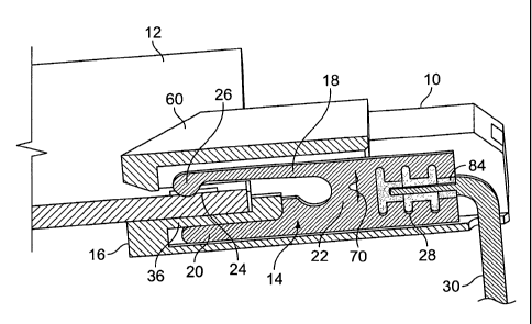
[0019] Referring first to Figures 1 and 2, a card (or edge cable connector
and PC card 12 are shown. Electrical contact elements 14 are inserted
within a housing portion 16. The housing portion 16 is an electrically
insulating
material. A high-temperature resin may be employed for applications that
expose the connector 10 to high temperatures, e.g., if the components of the
PC card 12 include high-temperature LEDs, or if the card or PC card
substrate has an aluminum core for heat dissipation.
[0020] Furcated contact elements 14 include an upper tine 18 and a lower
tine portion 20. The upper tine portion 18 and lower tine portion 20 are
joined
at one end by a web portion 22. The novel furcated design provides a high
normal contact force for reliable and stable connection to the plated contacts
24 of the PC card 12, while maintaining a tight contact-to-contact centerline
or
pitch. The web portion 22 provides a reinforced joint at the intersection of
they
upper and lower tine portions 18, 20, which is resistant to metal deformation
-3-
CA 02687719 2009-11-19
WO 2008/153889 PCT/US2008/007056
due to heat- and mechanically-induced stresses, as described in greater detail
below. A plated interface 26 aligns with the plated PC card contacts 24. The
contact base material may be a high-temperature copper alloy, e.g., phosphor
bronze, beryllium copper, or similar copper alloys with resistance to stress
relaxation, as will be known to those skilled in the art. A wire termination
portion 28 is disposed on the contact element 14 at the end opposite of the
tines 18, 20. Wires 30 have insulated jackets, a portion of which is stripped
from the end for electrically joining the wire 30 to the wire termination
portion
28. The wires 30 may be soldered, welded or crimped into the wire
termination portion 28.
[0021] The housing is designed to insulate the furcated contact lower tine
20 from the bottom and edge of the circuit board 12. An insulating layer 36 of
the housing 16 provides the electrical isolation of the lower tine 20 from the
PC card 12. In one embodiment, the PC card 12 has an aluminum core for
improved heat dissipation characteristics and rigidity. Alternatively, the PC
card 12 may comprise a conventional epoxy resin substrate.
[0022] Figure 3 is a mating end view of the contact portion of the connector
10. The forward end 50 has a slot 52 having a width approximately equal to,
or slightly greater, than the thickness of the PC card 12 substrate, so that
the
connector 10 engages with the PC card 12 in an interference fit with the
contact interface 26. Opposing surfaces 54, 56 adjacent either side of the
slot
52 are tapered from a wider dimension at front surface 50 to a narrower
dimension at the rear of the slot 52, to promote engagement of the connector
and PC card 12, and prevent interference when joining them together.
Also shown are the contact interfaces 26, which project downward into the
slot 52 from the top portion 60, to engage the plated contact pads 24 (See,
e.g., Figure 2). Detent latch 32 is disposed adjacent the forward edge 50 of
the connector.
-4-
CA 02687719 2009-11-19
WO 2008/153889 PCT/US2008/007056
[0023] Referring next to Figures 4 and 5, in one embodiment of the
connector 10 the detent latch 32 engages an aperture 34 positioned in the PC
card 12. The aperture 34 and detent latch 32 provide retention between the
housing portion 16 and the PC card 12. The detent latch 32 provides
additional retention force of the connector 10 to the PC card 12 that
supplements the friction retention imparted by the normal force of the contact
elements 14 in engagement with the PC card contact pads 24. The contacts
may be arranged at a predetermined pitch with respect to the PC card 12 for
facilitating alignment with the PC card 12.
[0024] Figure 6 is an isolated view of a contact element 14 apart from the
connector housing 16. The contact element 14 may be configured with a slot
38 having a projection 40 defining a secondary slot 42. The contact element
14 is retained within the housing by detent 70. Web portion 22 connects tines
18, 20, with sufficient cross-sectional area to inhibit angular flexing and
stress
relaxation of the tines 18, 20. The contact guide channel 66 (See, e.g.,
Figure 8) also restricts angular flexing of tines 18, 20 within the width of
the
guide channel 66. The tines 18, 20, contact interface 26, projection 40, wire
termination portion 28, slot 38, secondary slot 42, and other features of the
contact element 14 may be stamped from a flat metallic strip of copper or
copper-alloy, as described above.
[0025] Referring to Figure 7, an end view of the contact portion 14 shows
alternating beam portions 44,46 formed in the wire termination portion to
provide an aperture or solder cup 48 for inserting stripped wire ends 78 into
the wire termination portion 28, where the wire ends are soldered to the wire
termination portion 28 by a soldering material (designated by hashing 84). In
one embodiment, the alternating beams 44, 46 are formed outwardly on
opposing sides of the centerline of the contact portion 14 to allow for the
wire
to be aligned with the centerline of the contact portion 14 when inserted.
-5-
CA 02687719 2009-11-19
WO 2008/153889 PCT/US2008/007056
[0026] Referring next to Figure 8, a cross-sectional view through the
connector 10 shows the contact detent 70 engaging the shelf portion 62 of the
housing portion 16. The alternating beam portions 44, 46 of the contact
portion 14 are separated from the detent portion 70 by the shelf portion 62.
The shelf portion 62 latches the contact portion 14 into the housing portion
16
when the contact portion 14 is fully inserted into the guide channel 66. The
projection 40 abuts the end of guide channel 66 opposite the shelf portion 62,
to limit the penetration of the contact portion 14 in the housing portion 16.
[0027] Referring next to Figures 9 and 10, in one embodiment alignment
slots 72, 74 may be disposed on the PCB or mating cable connector 12, to
align. When the connector 10 is coupled together with the PCB 12, indicated
by arrow 76, housing wall 64 engages with alignment slot 72 to align them
relative to each other, and to ensure proper polarity. A second alignment 72
slot may be provided at the opposite end of the connector 10, for engaging a
housing wall 64. Alignment may be further ensured by aperture 34 if a detent
portion 32 is used to prevent the housing portion 16 from receding from the
PCB 12.
[0028] Referring next to Figures 11 and 12, in one embodiment there is a
novel configuration for the solder cup 48 that provides a soldered connection
(designated by the cross-hatching 84) that allows the soldered connections to
have a narrow profile, and thus enabling a smaller connector 10, or an
increased number of wires across the width of the connector 10. The wire 30
includes an insulation jacket 80 surrounding a conductor core 78. The jacket
80 is stripped away from the core 78 at an end portion 88, and the core 78 is
inserted, as indicated by arrow 82, into the solder cups 48 that are defined
between opposing beam portions 44 and 46. The wire is maintained
approximately at the axis or centerline of the contact portion 14 by the beam
portions 44 and 46 and solder cups 48. The core 78 may be inserted into
the solder cup 48 and soldered by conventional soldering means. Alternately
-6-
CA 02687719 2009-11-19
WO 2008/153889 PCT/US2008/007056
the core 48 may be pre-coated with a tin or tin alloy layer designed to re-
flow
when heated to bond the wire core 78 to the contact portion 14.
-7-