Note: Descriptions are shown in the official language in which they were submitted.
CA 02687775 2013-01-31
- 1 -
Fabrication of MEMS and MOEMS components
The invention relates to a method for the production of micromechanical, micro-
electromechanical (MEMS) or micro-opto-electromechanical (MOEMS) components,
and to such a component.
In order to minimize environmental influences such as moisture and
contaminants,
(e.g. dust) on micro-electromechanical components (MEMS) or micro-opto-
electromechanical components (MOEMS), active structures of such components are
often hermetically encapsulated. In this case, "active structure" should be
understood to mean, in particular, movable structures, optical structures or
structures having both movable and optical components (e.g. movable mirrors).
The
term "active region" denotes the region or volume of the component in which
the
active structure lies or moves. The hermetically tight encapsulation can
furthermore
be utilized for setting a specific internal pressure in the region of the
active
structures, which is advantageous particularly in components whose functioning
is
dependent on a defined internal pressure, such as e.g. acceleration sensors
and
gyroscopes (rate-of-rotation sensors).
In order that production can be implemented as cost-effectively as possible,
the
fabrication of MEMS or MOEMS components generally takes place at the wafer
level.
The joining processes that are often to be carried out in this case can be
effected for
example on the basis of direct bonding processes and anodic bonding processes.
Leading electrical contacts out from the hermetically tight region of the
component
in order to make contact with specific parts of the component (e.g. in order
to make
contact with the active structure) is difficult to
2
CA 02687775 2013-01-31
- 2 -
realize from the standpoint of fabrication technology. Various possibilities
are
considered: Electrical contacts can be realized for example by laterally
extending
semiconductor layers which are produced by means of implantation or diffusion
methods and have a low sheet resistance. Furthermore, a realization by means
of
patterned conductive layers covered with a planarized passivation layer is
possible.
As an alternative, the electrical contacts can be led out from the component
in the
form of a plurality of vertically extending plated-through holes.
DE102005015584 describes a method for the production of a component in which
the active region and hence the active structure of the component is isolated
from
the environment of the component (as far as contaminants and moisture are
concerned) before the contact holes are produced. Electric currents required
by the
active structure for the operation of the component and signals generated by
the
active structure are respectively fed to the active structure and tapped off
from the
latter via the contact holes and via the conductive structure layer adjacent
thereto.
However, the technology described does not enable any crossover of
interconnects.
In particular, it is not possible to make contact with regions (e.g.
electrodes) lying
within a movable structure that is closed (in a component layer plane) with a
tenably small area requirement. Therefore, the movable structures realized by
means of this technology in MEMS often have openings for the interconnects to
electrodes.
Therefore, the object of the invention is to specify a method for producing a
component, in particular a micromechanical, micro-electromechanical or micro-
opto-electromechanical component, and such a component
by
1 3
CA 02687775 2013-01-31
MOLLER = HOFFMANN & PARTNER - 3 -
Northrop Grumman LITEF GmbH - CA 2,687,775 File: 60536
means of which interconnect crossovers and in particular bridges over movable
structures can be realized.
The object is achieved according to the invention by means of a method for
fabricating a MEMS or MOEMS component and by means of a MEMS or MOEMS
component.
In this case, a first layer assembly is produced, which has a first substrate,
on said
first substrate a first insulation layer and on said first insulation layer an
at least
partly conductive covering layer, first depressions and second depressions are
produced in the covering layer, wherein the first depressions have a first
etching
depth and the second depressions have a second etching depth, which is smaller
than the first etching depth, and the first etching depth is at least equal to
the
thickness of the covering layer, and an at least partly conductive structure
layer is
applied to the covering layer in such a way that the structure layer adjoins
the
covering layer at least in regions.
So-called interconnect bridges are realized by the different etching depths,
the
structures being bridged by said interconnect bridges.
The method according to the invention increases the design freedom or the
design
diversity since new structures become possible. As a result of absent
openings, a
stiffer structure is brought about, which leads to the reduction of parasitic
movements and effects. Moreover, the number of bonding pads can be reduced,
thus
giving rise to lower costs as a result of a smaller area requirement and an
increase
in the yield
2 4
CA 02687775 2009-11-19
WO 2009/003542 - 4 -
PCT/EP2008/002503
or reliability.
In one preferred configuration of the method and of the
component, the active structure of the component
produced according to the invention is produced by
patterning the structure layer, wherein the patterning
can be effected before or after the application of the
structure layer to the first layer assembly. The
patterning can be effected, for example, by applying a
mask on the surface of the structure layer and
subsequently etching the structure layer. If the
structure layer is not patterned until after
application, then it is not necessary to take account
of any joining tolerances during the application of the
structure layer.
In accordance with further advantageous configurations
of the method and of the component, the application of
an encapsulation layer or of a second layer assembly
enables a hermetically tight encapsulation at the wafer
level with an adjustable internal pressure and
simultaneously affords the possibility of producing a
shield electrically insulated from the other electrical
contacts for protection against
external
electromagnetic interference fields. In this case, the
structure layer can also be part of the second layer
assembly, which furthermore has a second substrate and
a second insulation layer.
A simple access to the metal contact-making areas
through the encapsulation layer can be achieved by
means of contact holes produced in the encapsulation
layer before the application of the encapsulation layer
to the structure layer.
When using the second layer assembly, preferably, in
the side of the second substrate facing the structure
layer, before the application of the structure layer to
CA 02687775 2009-11-19
WO 2009/003542 - 5 -
PCT/EP2008/002503
the second layer assembly, third depressions are
produced, the lateral positions of which correspond at
least in part to the lateral positions of the contact
holes that are formed later in the second substrate.
The third depressions can be used as contact holes (or
at least as parts of the contact holes), in a later
process stage of the production method according to the
invention.
In an advantageous manner, in the side of the second
substrate facing the structure layer, before the
application of the structure layer to the second layer
assembly, fourth depressions are produced, the lateral
positions of which correspond at least in part to the
lateral positions of the active structure or the active
structure of the structure layer; the second
depressions can correspondingly likewise be produced at
these lateral positions. The second and respectively
fourth depressions enable a mechanical movement (e.g. a
vibration) of that region of the structure layer which
lies within the active region. Furthermore, the second
and respectively fourth depressions can be used for
setting specific parameters of the component: Since the
mechanical vibration quality under specific conditions
is dependent primarily on the pressure enclosed into
the component, on the geometry of the active (movable)
structure and on the direct surroundings thereof, it is
possible, for example, to influence the vibration
quality of a vibratory active structure in a targeted
manner through the choice of the extents of the second
and respectively fourth depressions. Thus, the
vibration quality is all the greater, the deeper the
second and respectively fourth depressions (for the
same pressure within the component).
In the case of a symmetrical arrangement as a result of
identical etching depths of the second and fourth
depressions, symmetrical gas surroundings of the
CA 02687775 2009-11-19
WO 2009/003542 - 6 -
PCT/EP2008/002503
movable active structure arise. This substantially
depresses resulting damping forces perpendicular to the
plane of the layers and parasitic movements resulting
therefrom.
If third depressions have been formed within the second
substrate, then it is possible, in order to form the
contact holes, proceeding from that surface of the
second substrate which is remote from the structure
layer, to remove at least part of the second substrate
as far as a vertical position corresponding to the
vertical position of the bottoms of the third
depressions. The third depressions are thus "opened"
and available as contact holes.
It is likewise possible for a portion of the first
depressions and a portion of the third depressions to
be situated above and respectively below the active
structure.
In one particularly preferred embodiment, the first and
second substrates and also the structure layer and the
covering layer are composed of silicon, However, the
invention is not restricted to this; other
materials/material combinations are also conceivable.
Silicon generally has the advantages of good mechanical
properties, high availability and well-developed
processing methods. If the components mentioned above
are composed of silicon, then this has the following
advantages: low thermal stress (this advantage is always
present if the two substrates and also the covering and
structure layers are composed of the same material) and
also little outgassing during the thermal joining
process (compared with Pyrex or SD2 (both materials are
glasses sold by the companies "Corning Glas" and "Hoya"
respectively), whereby pressures of less than 0.01 mbar
can be realized within the component.
CA 02687775 2009-11-19
WO 2009/003542 - 7 -
PCT/EP2008/002503
In an advantageous manner, the different etching depths
can be produced by means of a two-stage dry etching
step by means of a double mask.
By producing electrodes for the active structure at the
positions of the second depressions in/on the covering
layer, it is possible to realize buried electrodes that
can be used to detect and impress movements and forces
perpendicular to the wafer plane.
By means of a three-stage etching process, both buried
electrodes and interconnect bridges can be realized
jointly in one component.
The invention is explained in more detail by means of
exemplary embodiments with reference to the figures in
the drawing, in which
figure 1 shows a process sequence with steps 1-1, 1-2,
1-3, 1-4 and 1-5 for the patterning of depressions
having different etching depths with the aid of a
double mask,
figure 2 shows a process sequence of the method
according to the invention on the basis of sectional
illustrations 2-1, 2-2, 2-3 and 2-4,
figure 3 shows a schematic plan view of a
micromechanical sensor structure with openings for the
interconnects as in the prior art,
figure 4 shows a schematic plan view of a comparable
sensor structure according to the invention, which was
produced by the method according to the invention,
figure 5 shows a sectional illustration of a component
with a buried electrode,
figure 6 shows a sectional illustration of a component
with a buried electrode and with an interconnect
bridge,
figure 7a shows a further sectional illustration of a
component with an interconnect bridge along the
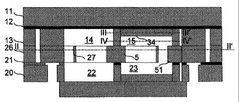
sectional area I-I' in figure 7b, and
CA 02687775 2009-11-19
WO 2009/003542 - 8 -
PCT/EP2008/002503
figure 7b shows a schematic cross section of a
component along the sectional area II-II' in figure 7a,
superimposed by a section along the area in
figure 7a (light gray shade) and a section along the
area IV-IV' in figure 7a (dark gray shade).
In the figures, identical or mutually corresponding
regions, components and component groups are identified
by the same reference numerals.
In the present invention, a so-called cover wafer 10,
in particular an SOI wafer (SOI: Silicon on Insulator),
can be used for example for a first layer assembly,
said wafer being patterned by means of a two-stage
patterning step, for example a two-stage dry etching
step (DRIE: Deep Reactive Ion Etching) using a double
mask. In this case, the SOI wafer 10 comprises a first
silicon substrate 11, a first insulation layer 12,
generally silicon dioxide, and a covering layer 13,
which is isolated from the first substrate 11 by the
buried first insulation layer 12.
Figure 1 illustrates how a first depression 14 having a
first etching depth D1 and a second depression 15
having a second etching depth D2 are realized (the
result is illustrated in step 1-5). Firstly, an oxide
layer 16 is realized on the SOT wafer 10 and patterned
(step 1-1). Afterward, a layer of photoresist 17 is
applied, exposed and developed (step 1-2). In the
following patterning step, the regions in the silicon
of the covering layer 13 are etched which have openings
at the same location in the oxide layer 16 and in the
photoresist mask 17, in the example at the lateral
position of the later first depression 14 (step 1-3).
After the first patterning step, the photoresist 17 is
removed (step 1-4). Openings in the oxide layer 16
which were previously covered with photoresist 17 are
uncovered in the process. In the second patterning
CA 02687775 2009-11-19
WO 2009/003542 - 9 -
PCT/EP2008/002503
step, these regions and the regions already patterned
in the first patterning step are etched into the
silicon of the covering layer 13. After the two etching
steps, the regions of the first depressions 14 which
had already been patterned in the first patterning step
have been opened down to the buried oxide 12 of the SOT
wafer, in order to enable an electrical insulation of
different electrodes. The depth of the second etching
step determines the later distance between a bridge and
the movable structure (or the interconnect in the
structure layer 26) (step 1-5), as can be seen below
with reference to figure 2. The buried oxide 12 acts as
an etching stop.
In the next step, the oxide 16 is removed (since the
silicon surface lying underneath is bonded later, the
removal is preferably effected wet-chemically). In this
case, the buried oxide 12 at the bottoms of the first
depressions 14 is also removed wholly (see figure 2-1)
or partly. However, this does not have a
disadvantageous effect on the function. The cover wafer
10 then has the structure illustrated in figure 2-1
with first depressions 14 having a first etching depth
D1, which corresponds to the thickness of the covering
layer 13 and thus extend at least down to the buried
oxide 12, and with second depressions 15 having a
second etching depth D2, which is smaller than the
first etching depth Dl.
In a next process step, a patterned second insulation
layer 21 is produced on the surface of a second
substrate 20. Afterward, third depressions 22 having a
third etching depth D3 and fourth depressions 23 having
a fourth etching depth D4 are produced in the surface
of the second substrate 20. In this case, the widths B1
of the third depressions 22 turn out to be smaller than
the widths B2 of the cutouts of the second insulation
layer 21 above the third depressions 22. In this way,
CA 02687775 2009-11-19
WO 2009/003542 - 10 -
PCT/EP2008/002503
break-off edges 24 arise in the regions adjoining the
third depressions 22, the function of which edges will
be described later.
In order to produce a second layer assembly 25, in a
next process step a structure layer 26 is applied to
the further insulation layer 21, wherein the structure
layer 26 bears on the individual regions of the second
insulation layer 21.
In a following process step, the structure layer 26 is
patterned in such a way that an active structure 27
arises, wherein outer regions 30 (the chip edge, that
is to say the edge region of the component to be
produced) of the structure layer 26 are electrically
insulated from the conductive regions "within" the
component by trenches 31. The construction illustrated
in figure 2-2 has then arisen.
In a next process step, the result of which is
illustrated in figure 2-3, the first layer assembly 10
and the second layer assembly 25 are joined together,
in such a way that the covering layer 13 adjoins the
structure layer 26 and the second depressions 15 and
the fourth depressions 23 are located above and
respectively below the active structure 27. What is not
illustrated but is likewise desired in part is the fact
that at least a portion of the first depressions 14 and
a portion of the third depressions 22 are also situated
above and respectively below the active structure 27.
During the bonding of the first layer assembly 10 onto
the second layer assembly 25 "SOI with buried
cavities", silicon is bonded onto a silicon rather than
a silicon being bonded onto oxide. Besides the
hermetically tight mechanical bond, a connection having
the lowest possible electrical resistance has to be
produced in this case.
CA 02687775 2009-11-19
WO 2009/003542 - 11 -
PCT/EP2008/002503
In a next process step, a bonding pad region 35 of the
second substrate 20 is etched back as far as a vertical
position corresponding to the vertical position of the
bottoms of the third depressions 22, with the result
that the third depressions 22 are uncovered and contact
holes 36 arise.
In the next process step, a metallization layer is then
deposited on the surface of the second substrate 20,
wherein, on account of the presence of the break-off
edges 24, that part of the metallization layer which is
deposited within the third depressions 22 is
electrically isolated from the rest of the
metallization layer, with the result that metal
contact-making areas 32 arise within the third
depressions 22. Afterward, contact is made with the
metal contact-making areas 32 by means of bonding wires
33, thus resulting in the structure in figure 2-4.
If desired, in a further process step, a further
metallization layer, a further metallization layer can
be deposited (not illustrated) on that surface of the
first substrate 11 which is remote from the structure
layer 26. The further metallization layer and also the
metallization layer serve as shielding electrodes for
shielding undesirable electromagnetic fields. The two
metallization layers can be connected to a defined,
common potential or to different potentials.
Accordingly, the invention has described a method for
producing micro-electromechanical or micro-opto-
electromechanical components, in particular components
having hermetically tightly encapsulated active
structures and areas for making electrical contact
therewith. The production method according to the
invention enables a hermetically tight encapsulation of
specific regions of the structure layer at the wafer
CA 02687775 2009-11-19
WO 2009/003542 - 12 -
PCT/EP2008/002503
level with an adjustable internal pressure and affords
the possibility of connecting the electrodes 5 in the
structure layer by means of interconnect bridges 34
over active structures 27, such as are shown by way of
example in figure 2-4, without having to provide
openings 3 as illustrated in figure 3. As a result, it
is possible to realize structures 1 as illustrated in
figure 4 in which the electrodes 5 can be contact-
connected via the interconnect bridges 34 (not
illustrated here) and, as a result, the structures 1
are not interrupted in comparison with the open
structures 6 in figure 3.
In order to insulate the conductive material of the
second substrate, use is advantageously made of break-
off edges 24 that bring about an electrical isolation
of the electrically conductive sidewalls of the contact
hole 36 from the bottom of the contact hole, said
bottom being connected (often directly) to an electrode
of the component.
The metallization of the contact regions is carried out
only after the conclusion of all the joining processes.
It is thus possible to use methods such as, for
example, silicon direct bonding (SDB) with temperature
loads of greater than 400 C provided that no doped
active regions exist within the structure layer 26, the
doping profiles of which could be impaired at
relatively high temperatures.
The invention can be applied to the production process
for any (miniaturized) components, in particular to the
production process for a micromechanical, micro-
electromechanical or micro-opto-
electromechanical
component, such as acceleration sensors, rate-of-
rotation sensors, pressure sensors, optical couplers,
etc.
CA 02687775 2009-11-19
WO 2009/003542 - 13 -
PCT/EP2008/002503
Figures 2-2 to 2-4 illustrate the optional case in
which the second substrate 20 is also patterned by
means of a two-stage DRIE step (before the realization
of the structure layer 26). In this case, the first
etching depth D1 and the third etching depth D3 are
chosen to be identical and the second etching depth D2
is also chosen to be identical to the fourth etching
depth D4. This has the advantage of symmetrical gas
surroundings of the active structure 27. This
substantially suppresses resulting damping forces
perpendicular to the wafer plane and parasitic
movements resulting therefrom.
If there is no need for a hermetically tight
encapsulation of the structures in the structure layer
26, the structure layer 26 can be realized on the
described first layer assembly 10 by means of SDB
(Silicon Direct Bonding) and can be pattered (after the
realization of bonding pads e.g. by means of aluminum
sputtering and etching).
It is also possible to realize a structure layer 26 on
the above-described first layer assembly 10 and
subsequently to pattern it. By means of SDB, anodic
bonding, anodic bonding with e.g. a sputtered Pyrex
interlayer or other joining methods, it is subsequently
possible to realize an encapsulation by means of an
encapsulation layer (e.g. a second substrate 20). In
this case, the encapsulation layer (e.g. 20) can be
prepatterned in order to ensure access to the metal
contact-making areas 32. This variant leads to cross
sections similar or identical to those shown in figure
2-4. In this way, the metal contact-making areas 32 can
be applied to the structure layer 26 actually prior to
the encapsulation, and the active structure 27 can be
tested. However, low-temperature joining methods should
then be used for the last joining process, in order to
prevent the metal contact-making areas 32 from being
CA 02687775 2009-11-19
WO 2009/003542 - 14 -
PCT/EP2008/002503
destroyed in this case.
Figure 5 illustrates that the two-stage patterning can
also realize buried electrodes 40, which can be used
primarily to detect and impress movements and forces in
the z direction (perpendicular to the wafer plane).
By means of a three-stage patterning with fifth
depressions 41 having a fifth etching depth D5, the
result of which is illustrated in figure 6, it is
possible to realize both buried electrodes 40 and
interconnect bridges 34.
In this case, the buried electrodes 40 are realized for
example by the material of the corresponding layer (the
covering layer 13) itself, or else by deposition of an
additional metallization layer on the corresponding
layer (the covering layer 13).
Figures 7a and 7b show a further illustration of a
component for the purpose of better elucidation. In
this case, figure 7a illustrates a schematic section
along the sectional area I-I' in figure 7b, while
figure 7b shows a schematic cross section along the
sectional area II-II' in figure 7a, superimposed by a
section along the area in figure 7a
(light
gray shade) and a section along the area IV-IV' in
figure 7a (dark gray shade). In this case, the cross
section in figure 7b shows particularly well the active
structure 27 and the interconnect bridge 34, which
connects an electrode 5 situated within the active
structure to a connection 51 outside the active
structure. In this case, the component illustrated also
shows an example of the fact that a portion of the
first depressions 14 and of the third depressions 22
are situated symmetrically above and respectively below
the active structure, as are the second depressions 15
and the fourth depressions 23. In the case of a
CA 02687775 2009-11-19
WO 2009/003542 - 15 -
PCT/EP2008/002503
symmetrical arrangement as a result of identical
etching depths of the second and fourth depressions 15,
23 and of the first and third depressions 14, 22,
symmetrical gas surroundings of the movable active
structure 27 arise. This substantially suppresses
resulting damping forces perpendicular to the plane of
the layers and parasitic movements resulting therefrom.