Note: Descriptions are shown in the official language in which they were submitted.
CA 02688179 2016-08-12
- 1 -
TELECOMMUNICATIONS CONNECTOR PANEL
WITH INTERPORT CROSSTALK ISOLATION
FIELD OF THE INVENTION
[0002] The present invention relates to multi-port telecommunication
connector
panels, specifically to measures for minimizing or preventing inter-port and
intra-port
crosstalk, and to measures for otherwise enhancing the performance of such
connector
panels.
BACKGROUND OF THE INVENTION
[0003] Due to advancements in telecommunications and data transmissions
speeds over balanced, twisted-pair cables, the connectors (such as jacks,
plugs, patch
panels, cross connects, etc.) are now a critical impediment to high
performance data
transmission at higher frequencies. Performance characteristics, particularly
crosstalk
and return loss, degrade beyond acceptable levels at higher frequencies. This
degradation is particularly true for system operation at category 6 and
category 6A
levels.
CA 02688179 2016-08-12
- 2 -
[0004] When an electric signal is carried on a signal line that is in close
proximity
to another signal line or lines carrying a signal or signals, such as in the
case of
adjacent pins of contacts in the connector, energy from one signal line can be
coupled
into adjacent signal lines by the electric field generated by the potential
between the
two signal lines and the magnetic field generated as a result of the changing
electrical
fields. This coupling, whether capacitive or inductive, is called crosstalk.
[0005] Crosstalk is a noise signal that degenerates the signal-to-noise
margin or
ratio (S/N) of the system. In telecommunication systems, reduced SN margins
result
in greater error rates in the information conveyed on the signal line. The SN
margin
must satisfy set performance criteria for the system category involved.
[0006] Crosstalk problems could be overcome by increasing the spacing
between
the signal lines, or by shielding the individual signal lines. In many cases,
the wiring
is preexisting and standards define the geometries and pin definitions for
connectors,
making the necessary changes to such systems cost-prohibitive. In the specific
case
of communication systems using balanced, twisted-pair wiring, standards
defining
connector geometries and pin out definitions are in effect, but were created
prior to
the need for high speed data communications.
[0007] These standards have created a large base of wiring and connectors
and a
need for connectors capable of meeting the requirements of high speed
communications, while maintaining compatibility with the original connectors.
The
standard connector geometries and pin outs are such that a great deal of
crosstalk
occurs at higher signal frequencies.
CA 02688179 2009-12-11
-3-
100081 Numerous connector constructions have been developed to address
crosstalk problems. Minimizing near end cross talk between the signal lines of
an
individual connector typically involves counteracting a noise signal in a line
by
inducing in that line a signal equal to and opposite to the noise signal such
that the
induced noise signal is effectively cancelled by the induced correction
signal.
Examples of such connectors are disclosed in U.S. Patent Nos. 5,432,484,
5,673,009
and 6,796,847, the subject matter of each of which is herein incorporated by
reference. Alien crosstalk between the conductors of adjacent connectors has
been
addressed by applying separate dedicated shielding components around
individual
connectors. See, e.g., patent application publication No. US 2009/0098777.
SUMMARY OF THE INVENTION
[00091 As used in this application, the terms "top", "bottom", "side",
"front",
"rear" and the like are intended to facilitate the description of the
electrical connector
panel and parts thereof. Such terms are merely illustrative of the connector
panel and
its parts, and are not intended to limit the connector panel and its parts to
any specific
orientation.
[00101 The invention utilizes electrically conductive housing portions and
barriers
that separate and serve to isolate adjacent ports and adjacent sets of
insulation
displacement contacts associated with different ports. As used herein to
describe such
housing portions and barriers, the term "electrically conductive" means
containing
conductive materials or elements that impart at least partial local
conductivity
substantially throughout such housing portions and barriers.
[0011] From one perspective, the invention is embodied in a
telecommunications
connector assembly comprising an electrically conductive housing defining at
least
one port having a plug receiving cavity. A set of jack contacts in the port is
adapted
to mate with respective contacts of an inserted connector plug, and is
electrically
connected to a set of insulation displacement contacts. The jack contacts are
substantially surrounded by and electrically insulated from the housing. An
electrically conductive isolation barrier is adjacent the set of insulation
displacement
CA 02688179 2009-12-11
- 4 -
contacts and is electrically connected to the housing. Thus, the isolation
barrier
would separate the sets of insulation displacement contacts of adjacent ports.
The
isolation barrier may be integrally formed with the housing.
[0012] From another perspective, the invention is embodied in a multi-port
telecommunications panel comprising a mounting circuit board, a plurality of
sets of
insulation displacement contacts on the circuit board, and a plurality of sets
of jack
contacts on the circuit board. Each set of jack contacts is electrically
connected to a
respective set of insulation displacement contacts and is adapted to mate with
respective contacts of an inserted connector plug. An electrically conductive
housing,
which is electrically insulated from the jack contacts, substantially
surrounds and
separates the sets of jack contacts to define a plurality of ports, each port
having a
plug receiving cavity aligned with a respective set of jack contacts. An
electrically
conductive isolation barrier is disposed between each pair of adjacent sets of
insulation displacement contacts. Each isolation barrier is electrically
connected to
the front housing. The isolation barriers may be integrally formed with the
housing.
The jack contacts and the insulation displacement contacts may extend from
opposite
sides of the circuit board, or from the same side of the circuit board.
100131 From yet another perspective, the invention is embodied in a multi-
port
telecommunications panel comprising a mounting circuit board having opposed
front
and rear faces; a plurality of sets of insulation displacement contacts
extending from
the rear face of the mounting circuit board; a plurality of sets of jack
contacts
extending from the front face of the mounting circuit board; and an
electrically
conductive front housing at the front face of the mounting circuit board
substantially
surrounding the sets of jack contacts individually and collectively to define
a plurality
of ports, each with a plug receiving cavity aligned with a respective set of
jack
contacts. Each set of jack contacts is electrically connected to a respective
set of
insulation displacement contacts and is adapted to mate with respective
contacts of an
inserted connector plug. The front housing is electrically insulated from the
jack
contacts and has an isolation barrier associated with each pair of adjacent
sets of
CA 02688179 2009-12-11
- 5 -
insulation displacement contacts. Each isolation barrier extends rearward
beyond the
mounting circuit board between the adjacent sets of insulation displacement
contacts.
[0014] Each set of jack contacts preferably is supported in a module having
an
electrically insulating frame. Preferably, adjacent insulation displacement
contacts of
adjacent sets of insulation displacement contacts are offset. And adjacent
insulation
displacement contacts of each set preferably are offset.
[0015] Each isolation barrier preferably comprises a pair of spaced
substantially
parallel plates occupying the region between the adjacent sets of insulation
displacement contacts. The plates preferably are paddle-shaped and are
substantially
congruent. Each isolation barrier preferably passes through a respective slot
in the
mounting circuit board. Each slot preferably is at an edge of the mounting
circuit
board. The front housing and the isolation barriers preferably are made of a
conductive thermoplastic resin.
[0016] An electrically insulating rear housing covers the rear face of the
mounting
circuit board and flanks the insulation displacement contacts. The rear
housing has an
opening aligned with each slot in the mounting circuit board, through which
opening
an isolation barrier extends. The rear housing is secured to the front housing
by
fasteners, such as screws, thus sandwiching the mounting circuit board
therebetween.
[0017] If the front housing does not completely cover the front of the
mounting
circuit board, an electrically insulating shroud can be provided that
surrounds the
front housing and covers the remainder of the front of the mounting circuit
board.
The shroud is secured to the rear housing, preferably by snap tabs that
project from
the shroud and engage mating shoulders on the rear housing.
[0018] The mounting circuit board has electrically conductive traces that
connect
the jack contacts to their respective insulation displacement contacts. The
mounting
circuit board preferably includes a ground plane for each port adjacent its
electrically
conductive traces for optimizing common mode impedance.
CA 02688179 2016-08-12
- 5a -
10018A1 In a broad aspect, the invention pertains to a multi-port
telecommunications
connector panel comprising a mounting circuit board having opposed front and
rear faces, a
plurality of sets of insulation displacement contacts extending from the rear
face of the mounting
circuit board, and a plurality of sets of jack contacts extending from the
front face of the
mounting circuit board. Each set of jack contacts is electrically connected to
a respective set of
insulation displacement contacts and is adapted to mate with respective
contacts of an inserted
connector plug, and an electrically conductive front housing at the front face
of the mounting
circuit board substantially surrounds the sets of jack contacts, individually
and collectively, to
define a plurality of ports. Each port has electrically conductive integral
wall portions of the
front housing defining a plug receiving cavity aligned with, and substantially
surrounding, a
respective set of jack contacts. The front housing is electrically insulated
from the jack contacts
and has an isolation barrier associated with each pair of adjacent sets of
insulation displacement
contacts, and each isolation barrier extends rearward beyond the mounting
circuit board between
the adjacent sets of insulation displacement contacts.
10018B1 In a further aspect, the invention provides a multi-port
telecommunications
connector panel comprising a mounting circuit board having opposed front and
rear faces, a
plurality of sets of insulation displacement contacts extending from the rear
face of the mounting
circuit board. A plurality of contact modules extend from the front face of
the mounting circuit
board, each contact module having a set of jack contacts electrically
connected to a respective set
of insulation displacement contacts and adapted to mate with respective
contacts of an inserted
connector plug. An electrically insulating rear housing covers the rear face
of the mounting
circuit board and flanks the insulation displacement contacts. The rear
housing is fastened to the
front housing, sandwiching the mounting circuit board and the contact modules
therebetween.
An electrically conductive front housing at the front face of the mounting
circuit board
substantially surrounds the contact modules, individually and collectively, to
define a plurality
of ports, each port having electrically conductive integral wall portions of
the front housing
defining a plug receiving cavity aligned with, and substantially surrounding,
a respective contact
module. The front housing is electrically insulated from the jack contacts and
has a rearward
CA 02688179 2016-08-12
5b
extending isolation barrier associated with each pair of adjacent sets of
insulation displacement
contacts. Each isolation barrier passes through a respective slot in the
mounting circuit board and
an aligned opening in the rear housing, and extends between the adjacent sets
of insulation
displacement contacts. An electrically insulating shroud surrounds the front
housing, and covers
the front of the mounting circuit board and is secured to the rear housing.
[0018C] In a
still further aspect, there is provided a multi-port telecommunications
connector panel comprising a mounting circuit board, a plurality of sets of
insulation displacement
contacts on the mounting circuit board, and a plurality of sets of jack
contacts on the mounting
circuit board. Each set of jack contacts is electrically connected to a
respective set of insulation
displacement contacts and adapted to mate with respective contacts of an
inserted connector plug.
An electrically conductive housing substantially surrounds and separates the
sets of jack contacts
to define a plurality of ports. Each port has electrically conductive integral
wall portions of the
front housing defining a plug receiving cavity aligned with, and substantially
surrounding, a
respective set of jack contacts. The housing is electrically insulated from
the jack contacts, and
an electrically conductive isolation barrier is disposed between each pair of
adjacent sets of
insulation displacement contacts, each isolation barrier being electrically
connected to the front
housing.
CA 02688179 2009-12-11
- 6 -
BRIEF DESCRIPTION OF THE DRAWING FIGURES
[0019] A preferred embodiment of the disclosed invention, which includes
the
best mode for carrying out the invention, is described in detail below, purely
by way
of example, with reference to the accompanying drawing, in which:
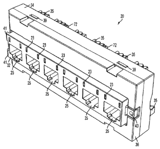
[0020] FIG. 1 is a front and top perspective view of the electrical
connector panel
with multiple shielded ports and shielded, offset insulation displacement
contacts
according to an exemplary embodiment of the present invention;
[0021] FIG. 2 is a front and bottom perspective view of the electrical
connector
panel of FIG. 1;
[0022] FIG. 3 is a rear and top perspective view of the electrical
connector panel
of FIG. I;
[0023] FIG. 4 is a rear elevation of the electrical connector panel of FIG.
1;
[0024] FIG. 5 is an exploded perspective view of the electrical connector
panel of
FIG. 1;
[0025] FIG. 6 is an exploded rear perspective view of the front housing and
two
contact modules of the electrical connector panel of FIG. 1;
[0026] FIG. 7 is a rear and top perspective view of the shroud of the
electrical
connector panel of FIG. 1;
[0027] FIG. 8 is an end perspective view in medial transverse cross-section
of the
electrical connector panel, taken along line 8-8 in FIG. 2;
[0028] FIG. 9 is an end perspective view in transverse cross-section of the
electrical connector panel, taken along line 9-9 in FIG. 2;
[0029] FIG. 10 is a perspective view of a contact module of the electrical
connector panel of FIG. 1;
[0030] FIG. 11 is a different perspective view of a contact module of the
electrical
connector panel of FIG. 1;
[0031] FIGS. 12-15 are top plan views of the conductive trace layers of the
mounting circuit board of the electrical connector panel of FIG. 1; and
[0032] FIG. 16 is a front perspective view of eight electrical connector
panels
according to FIG. 1, installed in a common metal support panel.
CA 02688179 2009-12-11
- 7 -
DETAILED DESCRIPTION OF THE INVENTION
[0033] Referring to FIGS. 1-8, the electrical connector panel 20 of the
invention
has at its core a mounting circuit board 22 that supports six contact modules
24, which
extend from the front face 26 of circuit board, and six sets of insulation
displacement
contacts (IDCs) 28, which extend from the rear face 30 of the circuit board.
Each set
of eight IDCs is electrically connected to the eight jack contacts 29 of a
respective
contact module 24 via electrically conductive traces on the circuit board 22
(see FIG.
13). Contact module 24 has an electrically insulating frame 31 supporting jack
contacts 29.
[0034] A front (nose) housing 32, preferably molded of a conductive
thermoplastic material, covers the contact modules 24. The material for the
front
housing 32 preferably is a stainless steel fiber filled thermoplastic resin. A
preferred
example of such material is a thermoplastic marketed under the name FARADEX by
SABIC Innovative Plastics of Pittsfield, Massachusetts. Alternatively, front
housing
32 could be completely metallic. Front housing 32 has six port openings 25
into
respective plug receiving cavities 27, each aligned with the jack contacts of
a
respective contact module 24. Two mounting slots 23 above each port opening
accommodate a port identification label. Front housing 32 also has hooks 41 at
one
end, and a tab with a screw hole 43 at the opposite end, that facilitate
mounting the
connector panel 20 in a common metal support panel (see FIG. 16).
[0035] A rear housing 34, molded of an insulating thermoplastic material,
covers
the rear face 30 of the circuit board and has portions 35 that extend rearward
and flank
the IDCs 28. Fasteners, preferably in the form of screws 38, pass through
holes 40 in
rear housing 34 and holes 42 in circuit board 22, to threadably engage blind
holes 44
in the back of front housing 32. An insulating molded plastic shroud 36
surrounds
front housing 32 and covers the remainder of the front face 26 of the circuit
board.
Shroud 36 has resilient snap tabs 37 that mate with recesses 39 in rear
housing 34.
Shroud 36 could be eliminated if the front housing 32 were broad enough to
cover the
entire circuit board 22.
CA 02688179 2009-12-11
-8-
100361 The screws 38, which secure the front and rear housings together,
force the
sandwiched mounting circuit board 22 into position against front housing 32 to
take
up tolerances. Referring to FIGS. 5, 6 and 8, proper alignment of front
housing 32
and circuit board 22 is ensured by end locating pins 46 on front housing 32
that
engage mating end locating holes 48 in circuit board 22, and by a central
locating pin
50 on front housing 32 that engages a mating central locating hole 52 on
circuit board
22. Each screw hole 40 in rear housing 34 is surrounded by a boss 54 that
abuts the
rear face 30 of the circuit board 22 to ensure a tight assembly (see FIG. 8).
[0037] Front housing 32 has interlocking features that ensure proper
alignment
with contact modules 24, thus ensuring proper mechanical functioning of the
contact
system. Referring to FIGS. 10 and 11, each side of the insulating frame 31 of
contact
module 24 has a lateral shoulder 56 adjacent a circuit board locating pin 58
(which
engages a mounting hole 59 in circuit board 22), and a tapered side wall 60.
Referring to FIG. 6, end walls 62 and intermediate walls 64 of front housing
32 are
spaced to closely receive contact modules 24 at six locations 66. As viewed in
FIG.
6, the contact modules 24 (only two are shown for the sake of clarity) are
positioned
with their locating pins 58 facing up and their electrically conductive jack
contacts 29
facing left, toward plug receiving cavities 27. Each end wall 62 and each
intermediate
wall 64 has a notch 68 sized to embrace a lateral shoulder 56 of a contact
module 24,
and a tapered recess 70 sized to embrace an upper tapered side wall 60 of a
contact
module 24. Thus, when rear housing 34 is secured by screws 38 to front housing
32
with mounting circuit board 22 sandwiched therebetween, contact modules 24 are
snugly positioned in notches 68 and recesses 70.
100381 Front housing 32 also has four isolation barriers 72 cantilevered
from its
elongated walls 74. Isolation barriers 72 extend rearward through edge slots
76 in
mounting circuit board 22, through aligned openings 78 in rear housing 34, and
between adjacent sets of IDCs 28. Each isolation barrier 72 comprises a pair
of
spaced, congruent paddle-shaped plates 73 separated by an air gap 75.
Referring to
FIG. 4, the IDCs 28 are arranged in two rows (upper and lower) of three sets
each,
each set having four pairs of IDCs (for connection to twisted pair cabling).
Two
CA 02688179 2009-12-11
- 9 -
isolation barriers 72 extend between the adjacent sets of IDCs of each row,
thus
separating the IDC sets associated with their three respective ports and
contact
modules 24. The IDCs are also arranged in an offset pattern of pairs.
Specifically,
each pair of IDCs is offset from any adjacent pair, both within and between
each set.
Accordingly, no two pairs of IDCs directly flank each other, which helps to
separate
twisted pairs and reduce crosstalk.
[0039] The electrically conductive nature of front housing 32 is inherent
in all of
its parts. Thus, intermediate walls 64 shield the contacts of adjacent contact
modules
from one another, minimizing alien crosstalk at the ports. Further, the face
and the
surrounding walls 62, 74 of front housing 32 shield the contacts of all ports
from
extraneous electromagnetic interference. In addition, the isolation barriers
72
between the sets of IDCs provide improved crosstalk isolation. A solid barrier
would
function to provide some improvement (reduction) in the level of alien
crosstalk (as
compared to no barrier) because of the solid barrier's shielding effect, but
it would
still result in secondary capacitive coupling between adjacent IDCs. Split
isolation
barriers with an intermediate air gap 75 between plates 73 are preferred
because they
provide better crosstalk isolation by further reducing the coupling and,
therefore, alien
crosstalk.
[0040] Several structures electrically insulate the jack contacts 29 of
each contact
module 24 from the conductive front housing 32. Referring to FIGS. 10 and 11,
the
jack contacts 29 are mounted in an electrically insulating overmold 80, from
which
the compliant pin terminal ends 82 of jack contacts 29 protrude. Pin terminals
82
extend through holes 84 in the mounting circuit board 22 and electrically
connect to
conductive traces therein (see FIG. 13). Electrically insulating frame 31 has
a
proximal portion 86 surrounding and supporting overmold 80, a central portion
87
flanking the jack contacts 29, and a distal portion 88 with comb-like teeth 90
that
separate the other ends of jack contacts 29. Further, an electrically
insulating spring
retainer 92 for a spring 94 embraces the central portion 87 of the frame.
Spring 94
resiliently supports a compensation circuit board 96 having separate contacts
(not
CA 02688179 2009-12-11
- 10-=
shown) that connect with jack contacts 29 when a connector plug is inserted
into the
plug receiving cavity 27.
[0041] Details of the spring-biased compensation circuit board and contact
arrangement are disclosed in the aforementioned Application Serial No.
12/314,613.
Crosstalk compensation typically is applied to the connectors at one or more
of three
locations in the manner described in Application Serial No. 12/314,613,
namely: (1)
near the distal ends of the jack contacts through the spring-mounted
compensation
circuit board 96, (2) at the jack contact mounting locations through the
mounting
circuit board 22, and (3) at the IDC locations through the mounting circuit
board 22.
Compensation can be applied at other locations as would be understood by those
skilled in the art.
[0042] FIGS. 12-15 separately depict the four superposed layers of
conductive
traces that comprise the electrical circuitry in mounting circuit board 22.
The
superposed conductive traces of different layers are electrically insulated
from each
other in a manner that would be readily recognized by one skilled in the art.
These
figures also depict mounting holes 97 for the IDCs 28, mounting holes 59 for
the
contact modules 24, and holes 84 for the pin terminals 82 of the jack
contacts. All of
the holes 84 are aligned because the ports 25 and the contact modules 24 are
aligned.
[0043] FIG. 13 depicts the fourth (bottom) layer with the main signal
traces 98
that connect to jack contacts 29 via pin terminals 82, which extend through
holes 84.
FIG. 12 depicts the third layer (disposed just above the bottom layer) that
has ground
planes 100 located directly above major portions of the main signal traces 98
(FIG.
13). This adjacent arrangement optimizes common mode impedance to improve
common mode return loss and reduce noise reflections and associated excess
alien
crosstalk normally observed when connectors are in close proximity to each
other
along the length of a cabling link. FIG. 15 depicts the second layer, which is
disposed
above the third layer of FIG. 12. FIG. 14 depicts the first (top) layer, which
is
disposed just above the second layer of FIG. 15. The spacing between the
second and
third layers preferably is greater than the spacing between the first and
second layers,
and greater than the spacing between the third and fourth layers.
CA 02688179 2009-12-11
- Ii -
[0044] Compensation elements and related traces are present in all layers
of the
circuit board 22. The compensation elements are in the form of plates 102. The
sizes
and relative positions of the compensation plates provide appropriate
capacitive and
inductive coupling for cancellation of crosstalk induced in other portions of
the
electrical connector panel.
[0045] The preferred embodiment of the invention illustrated and described
herein
is merely an example. It will be understood by those skilled in the art that
other
embodiments incorporating various changes and modifications also are
considered to
be within the scope of the invention, which is defined in the appended claims.
For
example, and without limitation, the electrically conductive front housing may
be
formed separately from the electrically conductive isolation barriers, with
provision
made for the barriers and the front housing to become electrically connected
when the
connector panel is assembled. The isolation barriers, whether integral with or
separate from the front housing, could extend around, rather than through the
mounting circuit board. For a front-access connector panel, in which the
insulation
displacement contacts and the jack contacts are on the same (front) face of
the
mounting circuit board, the isolation barriers would be fully disposed in
front of the
mounting circuit board. The number of ports can be fewer or greater than the
six
ports of the preferred embodiment; and the number of jack contacts per set can
be
fewer or greater than the eight jack contacts per set of the preferred
embodiment.