Note: Descriptions are shown in the official language in which they were submitted.
CA 02689508 2009-12-02
WO 2008/157080 PCT/US2008/066075
SOLID STATE ILLUMINATION DEVICE
FIELD OF THE INVENTION
The present invention relates to the field of general illumination, and more
specifically, to
illumination devices that use light sources as for example light emitting
diodes (LEDs) or
semiconductor lasers.
BACKGROUND
Solid state light sources are not yet frequently used for general illumination
due to
limitations in operating temperature, color rendering performance, color
consistency, and
efficiency. By way of example, solid state light sources with an input power
range of 10W to
40W have a high operating temperature and accordingly require the use of
relatively large heat
spreaders and cooling structures. Moreover, LEDs have a limited spectral
bandwidth, and thus,
color rendering performance is limited due to only a limited number of
efficient phosphors that
have been found. Additionally, the use of phosphors in proximity to the LED
limits the choice
of phosphors due to temperature and chemical incompatibility. Color
consistency is also
problematic due to production tolerances in the wavelength conversion
materials application
process and variations in the wavelength conversion materials itself. Finally,
compared to
conventional gas discharge lamps, the cooling efficiency of conventional solid
state light sources
is low and, thus, large cooling structures are required.
The source of solid state light sources, e.g., LEDs and lasers, operate at low
temperature
(in the range of 60 -200 C) relative the temperature of the sources in other
types of lighting, e.g.,
the filament in an incandescent bulb, the cathodes in a gas discharge base
fluorescent lamps, or
the plasma in an high intensity discharge lamp. The high temperature of these
conventional
sources causes most of the heat generated by the lamp to radiate to ambient
and spread out over a
large area. The lower operating temperature of LEDs, which results in less
heat radiating to
ambient, renders it difficult to use LED lamps in existing lighting fixtures
at same input power as
conventional light sources because the LEDs require higher capacity cooling
structures.
Fortunately, in most cases, the input power of LED systems can be lower than
that used for
conventional light sources, as state of the art LEDs have become more
efficient than
incandescent lamps (in produced light output versus electrical power in), and
soon will become
more efficient than the gas discharge based conventional lamps, but cooling
efficiency remains a
factor in adopting solid state light sources.
CA 02689508 2009-12-02
WO 2008/157080 PCT/US2008/066075
The engineering and manufacturing investments required to overcome the
challenges in
solid state light source applications renders that the costs of solid state
illumination installations
high compared to that of conventional light source solutions. As a result, the
introduction of an
efficient and environmentally safe solid state illumination technology has
been delayed.
Accordingly, what is desired is an illumination device, which includes
solutions to many of the
drawbacks mentioned before, and which can be used and installed in the
existing infrastructure.
SUMMARY
A solid state illumination device, in accordance with an embodiment of the
present
invention includes a semiconductor light emitter mounted on a base and
surrounded by at least
one sidewall. The base includes electrical connections for the semiconductor
light emitter as
well as a heat spreader that is thermally coupled to the semiconductor light
emitter. A reflective
top is coupled to the at least one sidewall such that a chamber is defined by
the base, top and the
at least one sidewall. At least 70% of light that is emitted from the chamber
is emitted from the
sidewalls of the chamber.
In another embodiment, a solid state illumination device includes a
semiconductor light
emitter mounted on a base and surrounded by at least one sidewall. A top is
coupled to the at
least one sidewall such that a chamber is defined by the top, base and the at
least one sidewall.
An adjustable wavelength converting element is coupled to the chamber and is
configured to
adjust a surface area that is exposed to light emitted by the semiconductor
light emitter in the
chamber to alter an optical property of the chamber, such as the color or
intensity of the light
output. In one embodiment, one of the top and the base includes an aperture
through which the
adjustable wavelength converting element is adjustably extended into the
chamber. The
adjustable wavelength converting element may be a rod with wavelength
converting material
coupled to the rod. In one embodiment, the rod includes an expandable portion
that expands and
constricts, e.g., to expand or constrict the length or the diameter.
In another embodiment, a solid state illumination device, in accordance with
an
embodiment of the present invention includes a semiconductor light emitter
mounted on a base
and surrounded by at least one sidewall. The base includes electrical
connections for the
semiconductor light emitter as well as a heat spreader that is thermally
coupled to the
semiconductor light emitter. The base and at least one sidewall define a
chamber that has a
height to diameter ratio is 2 or greater.
-2-
CA 02689508 2009-12-02
WO 2008/157080 PCT/US2008/066075
BRIEF DESCRIPTION OF THE DRAWINGS
Fig. 1 shows a solid state illumination device with a semiconductor light
emitter in
accordance with an embodiment of the present invention.
Figs. 2A and 2B show side views of a solid state illumination device in
various states of
assembly.
Figs. 3A, 3B, and 3C show the wavelength conversion material on the top
element of the
device.
Fig. 4 shows a solid state illumination device with a semiconductor light
emitter in
accordance with another embodiment of the present invention.
Fig. 5 shows a simplified view of a solid state illumination device.
Figs. 6A and 6B show the results of a simulation of the performance of a solid
state
illumination device and the efficiency of function of the height/diameter
ratio.
Figs. 7A and 7B shows additional embodiments of solid state illumination
devices.
Figs. 8A and 8B show cross-sectional views of solid state illumination devices
without a
separate top element in accordance with another embodiment of the invention.
Figs. 9A and 9B show alternative shapes for the sidewalls of the device.
Figs. 10A and 10B show side views of another embodiment of a solid state
illumination
device in various states of assembly.
Figs. 11A, 11B, and 11C show an adjustable wavelength converting element and
the
operation of the adjustment wavelength converting element with a solid state
illumination device
in accordance with another embodiment of the present invention.
Figs. 12A and 12B show an embodiment of an adjustable wavelength converting
element
that is manually adjustable.
Figs. 13A and 13B show an embodiment of an adjustable wavelength converting
element
that is adjustable by an actuator.
-3-
CA 02689508 2009-12-02
WO 2008/157080 PCT/US2008/066075
Figs. 14A, 14B, 14C, 14D, and 14E show alternative embodiments of an
adjustable
wavelength converting element.
Figs. 15A, 15B, 15C, and 15D show alternative embodiments of an adjustable
wavelength converting element.
Figs. 16A and 16B show an alternative embodiment in which the top element is
the
adjustable wavelength converting element.
Fig. 17A shows an embodiment of a solid state illumination device used with a
reflector
element to form a reflector lamp.
Fig. 17B shows the resulting intensity profile from the reflector lamp
illustrated in Fig.
17A.
Figs. 18A and 18B show additional embodiments of a solid state illumination
device used
with a reflector element to form a reflector lamp with an adjustable
wavelength converting
element is used.
Figs. 19A, 19B, and 19C show the use of a solid state illumination device as a
backlight.
Fig. 20A shows an application of the solid state illumination device.
Fig. 20B illustrates the use of an adjustable wavelength converting element
with an
illumination device such as that illustrated in Fig. 19B.
Figs. 21A and 21B show a candle type lamp bulbs used with a solid state
illumination
device.
Figs. 22A, 22B, 22C, 22D, and 22E show different bulb shapes that can be used
with a
solid state illumination device and mounting the bulbs so the device.
Fig. 23 shows a close-up view of the screw attachment of a bulb used with a
solid state
illumination device.
DETAILED DESCRIPTION
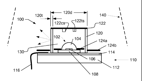
Fig. 1 illustrates a side view of a solid state illumination device 100, in
which at least one
semiconductor light emitter 102, such as a light emitting diode (LED), is
used. The
semiconductor light emitter 102 is referred to herein as light emitting diode
102 or LED 102,
-4-
CA 02689508 2009-12-02
WO 2008/157080 PCT/US2008/066075
interchangeably. In one embodiment, the LED 102 includes a lens 104, and may
be produced
by, e.g., Philips Lumileds Lighting LLC as the Luxeon Rebel or Luxeon K2.
Other
commercially available semiconductor light emitters can be used if desired, as
for example, those
produced by Nichia (Japan), Cree (USA), Osram (Germany), and Toyoda Gosei
(Japan).
Although semiconductor light emitters produced by these different
manufacturers come in
different forms sizes, and attachment methods, all can be made to fit into the
illumination device
100 shown in Fig. 1.
Moreover, although the semiconductor light emitter 102 is shown with a lens
104,
semiconductor light emitters without a lens can be used as well, as for
example the Luxeon Flash
LED, as produced by Philips Lumileds Lighting LLC, or the Ostar LED device, as
produced by
Osram. The Ostar device is an example of an LED where multiple dies are used
in a package.
The LED 102 typically, but not necessarily, consists of a light emitting
element, called the LED
die, or LED chip 106, and a chip carrier, called submount 108. If desired,
multiple
semiconductor light emitters may be used.
As illustrated in Fig. 1, the LED 102 is mounted on a base 110, which in this
embodiment
consists of a printed circuit board 114, and a heat spreader 112. In one
embodiment, a metal core
printed circuit board (MC-PCB) may be used, such as that manufactured by CIRE,
Bree
Industries. With some LEDs (as for example the Luxeon K2), it is possible to
directly mount the
LED 102 on heat spreader 112 (by gluing, or soldering, or using thermal paste
or tape), and to
connect the leads to a connection pads on a regular PCB (made for example of
FR4 material), or
directly solder wires to the LED leads. The heat spreader 112 may be
manufactured by, e.g.,
Aavid Thermalloy, USA, or by ThermalFlo Inc. Typically heatsinks are extruded
aluminum and
may be e.g., so-called Radial Extrusions, which consist of a central core and
radially placed fins.
The heat sink 112 should have low thermal resistance, preferably below 10 K/W
for LED powers
up to 5W and below 5 K/W for total LED input power up to 10W, and below 2 K/W
for total
LED input power up to 25W. The heat sink 112 may consist of multiple parts,
and the parts can
be of different shapes and sizes. The heat sink 112 may also be integrated
with, or form the
housing of a lighting fixture. In addition to the LED, the base 110 might
contain other electronic
parts (not shown), as for example a temperature sensor (e.g. NTC Thermistor),
or an optical
RGB sensor (as for example made by Hamamatsu (Japan), part number S10170).
Furthermore,
base 110 might contain an LED driver, as for example MAX16803 or MAX 16819, as
made by
Maxim (USA), and the components required in combination with these drivers. In
addition the
-5-
CA 02689508 2009-12-02
WO 2008/157080 PCT/US2008/066075
base 110 contains an electrical connection 116 to electrically connect the
illumination device 100
to a power supply or to a socket.
The illumination device 100 includes at least one sidewall 120 that may have a
circular,
elliptical, triangular, rectangular, or polygon shape as viewed from the top
and may be made of
an optical transparent or translucent material, glass, plastic, and/or A102.
The use of A102 as a
material for the sidewall 120 is advantageous because of its high thermal
conductivity, and high
optical transmission properties. The A102 can be mixed into a plastic, but
also used in pure
form, as for example in a ceramic form (Alumina), or in crystalline form
(Sapphire) For
example, when the sidewall 120 has a circular or elliptical shape, a single
continuous sidewall
may be used. When a triangular, rectangular or other similar discontinuous
shape is used,
separate sidewall sections may be used, and for the sake of simplicity, the
present disclosure will
refer to sidewalls 120. In one embodiment, portions of the sidewalls 120 may
be continuous,
while other portions are discontinuous, e.g., to form a configuration having a
"D" shape. In one
embodiment, the sidewalls 120 may be produced from a plastic such as PC (poly
carbonate),
PMMA (acrylic), or Zeonex (made by Zeon Corporation, Japan), which can be
mixed with metal
oxide particles as for example Mg02 or A102 to make the material more
scattering. The plastic
and metal oxide particles can be injection molded or extruded. The thickness
120t of the
sidewalls 120 may be in the range of, e.g., 0.1 to 3 mm. The diameter 120d of
the sidewalls 120
depends on the size of the LED 102, or the number of LEDs used, but may be in
the range of 3 to
13 mm.
The illumination device 100 may include a top element 122 that is made, e.g.,
of an
optical material with a high reflection (preferably at least 80% reflective),
and might be
reflecting in a diffuse way, as for example obtained with a material made by
Furukawa (Japan)
called MC-PET, or might have specular reflecting properties as for example
obtained with
material made by Alanod (Germany), with the brand name Miro, or might have a
combination of
specular, and diffuse reflection. Several materials made by Alanod have a
combination of
diffuse and specular reflecting properties, or a diffuse effect can be created
on a specular
reflecting material by screen printing white dots on a mirror, and by varying
the density and size
of the dots. Screen printing the dots can be used to achieve a high efficiency
or uniformity. Top
element 122 may contain microstructures, to control the efficiency and
uniformity. Additionally,
top element 122 may contain electronic parts as well, as for example a color
sensor 122cs (as for
example made by Hamamatsu, Japan, part number S10170) or temperature sensor
122ts (NTC
Thermistor). These electronic parts may be connected to the base 110 by thin
electrical wires
-6-
CA 02689508 2009-12-02
WO 2008/157080 PCT/US2008/066075
(not shown) running approximately in the middle of the chamber, 130 defined by
the top element
122, sidewalls 120, and the base 110, and are preferably coated with a highly
reflective white
coating, or, might be coated with a wavelength converting material like
phosphors.
The illumination device 100 may have reflective members 124a and/or 124b. As
with the
top element 122, the reflective members 124a and/or 124b may have a high
optical reflection and
low absorption, and have either specular and/or diffuse reflecting properties,
and may contain
microstructures to control the light distribution of the reflected light. To
avoid blocking light
from the LED 102 by the edges of the reflective members 124a and 124b, the
reflective members
124a and 124b may be thin and closely fit around the emitting area of the LED
102. By way of
example, the reflective members 124a and 124b from material manufactured by 3M
(USA), such
as Vikuiti Enhanced Specular Reflector (ESR film), which has a high
reflectivity and has a
thickness of about 65 micrometer and is flexible, which is useful to achieve a
close fit around the
LEDs without damaging the LEDs, or the LED lenses. Example of a thin diffuse
reflecting
material is E60L, which is made by Toray (Japan).
In one embodiment, the illumination device 100 may be used as a backlight,
e.g., with
red, green and blue LEDs 102 used, in combination with a feedback sensor 122cs
and/or 122ts
mounted on the top element 122.
Figs. 2A and 2B illustrate side views of another embodiment of a solid state
illumination
device 150, which is similar to illumination device 100 shown in Fig. 1, like
designated elements
being the same. Fig. 2A illustrates the assembly of the illumination device
150 and Fig. 2B
illustrates an illumination device 150 in an assembled form.
In this embodiment the reflector member 124 is attached to sidewall 170, using
a
mounting plate 172, which is designed to fit to the base 110 upon which is
mounted the LED
102. The reflective member 124 in this embodiment may be made of a thin,
flexible material
such as Vikuiti Enhanced Specular Reflector (ESR film), as made by 3M, which
has a high
reflectivity and has a thickness of 65 micrometer, or E60L, as made by Toray
(Japan), which is a
highly diffuse white reflecting film, and has a thickness of 188 micrometer.
By using a thin,
flexible material for reflective member 124 damage of the LED 102 during
mounting is avoided.
Further, by using a very thin material, almost no light from the LED 102
(emitted parallel to the
support structure 110) is blocked by the edge of the reflective member 124.
-7-
CA 02689508 2009-12-02
WO 2008/157080 PCT/US2008/066075
The top element 180 in this embodiment has an edge 182, which fits into the
sidewall
structure 170, and is fixed by either press fitting, gluing, click-fit, or
screw-in assembly. If
desired, the top element 180 may include a wavelength conversion layer 184 on
a top reflector
186. The wavelength conversion layer 184 can be either a uniform layer, with
the wavelength
conversion material embedded in a binder, or may consist of dots on the top
reflector 186, as
shown in Figs. 3A, 3B and 3C. The dots may be produced, e.g., by screen
printing. The
wavelength conversion layer 184 may include one or more phosphor material,
such as an amber
or a red light emitting phosphor, a combination of an amber and red light
emitting phosphor, a
yellow or green light emitting phosphor as well or combinations thereof.
One method of manufacturing the top element 180 with a wavelength conversion
layer
184 is to screen print a large plate of this material, and stamp out the top
elements with the
desired shape. As illustrated in Figs. 3A and 3B, the wavelength converting
layer 184 may be
formed on the top reflector 186 (or another material that is mounted on the
top reflector 186)
from a different numbers (and/or sizes) of dots 185 of a wavelength converting
material. As
illustrated in Fig. 3C, different wavelength converting materials may be used
to form dots 185a
and 185b. Alternatively, a mixture of wavelength converting materials may be
used to form each
dot, which provides a high degree of color point tunability, and improves the
so called color
rendering index, by creating a more continuous and flat spectrum. The dots 185
can be applied
to the top reflector 186, for example, by screen printing, or ink-jet
printing. While a relatively
small number of dots are illustrated in Figs. 3A-3C, it should be understood
that in practice a
large number of dots can be used with these techniques, which helps to get a
uniform reflection
from the top element 180.
The sidewall 170 include a transparent internal wall 132 attached to the
mounting plate
172 and a wavelength conversion layer 171 mounted to the internal wall 172.
The wavelength
conversion layer 171 can be either a uniform layer, with the wavelength
conversion material
embedded in a binder, or may consist of a number of dots on the internal wall
172. If desired,
the wavelength conversion layer 171 may be on the inside of the internal wall
172. The side wall
can be either a single piece, with the phosphor embedded in a plastic material
in the material
which is extruded (like in the production of colored drinking straws), or the
phosphor might be
applied to the inside or outside of a transparent or translucent cylindrical
carrier. If the phosphor
is applied onto a 'carrier tube', the phosphor is preferably applied to the
inside of the tube, to
avoid damages to the phosphor layer. The outside of the tube is preferable
made rough (by
etching, or sanding, or grinding), or has a micro structure.
-8-
CA 02689508 2009-12-02
WO 2008/157080 PCT/US2008/066075
An important aspect of this embodiment is the ability to combine different
top, side, and
bottom sections, with different colors of the solid state light emitting
device, and different
wavelength converting combinations, wavelength converting layer thicknesses,
wavelength
converting concentrations, and/or different coverage factors for the side and
top elements 13 and
12. Given the characteristics of the primary light emitter 11, and the
requirements of the
application, an appropriate sidewall 13 is chosen with known characteristics,
as well as a top
element 12, so that an illumination device is created with a color point,
color rendering index,
and spatial light output according to customer's demand as closely as
possible. Different bottom
sections can be used, with different solid state illumination emitters, which
allows to switch
suppliers depending on availability of primary light emitting devices 11,
without having to
change the specifications of the product, or, to use bulk of primary light
emitting devices
manufactured by a particular supplier, which vary in wavelength, light output,
and/or forward
voltage, by carefully selecting and combining the different emitters, side and
top elements, given
the target specifications of a device. This is for example done by using a
computer model of the
device, accessing a database of available parts.
Fig. 4 illustrates a side view of another embodiment of an illumination device
200,
similar to illumination device 150, like designated elements being the same.
Illumination device
200 includes multiple LEDs 202 in the form of an LED chips 204A and 204B
mounted on a
submount 206, a reflective member 208 attached to the submount 206 around the
chip 204,
sidewall section 210 placed around the chip 204 and the reflective member 208
and attached to
the submount 206. If desired, more or fewer LEDs may be used. The top elements
180 may be
configured similarly to that shown in Fig. 2A. The illumination device 200
contains a
transparent optical materia1214 within the chamber 213 defined by the submount
206 and the
sidewall section 210. The transparent optical materia1214 may be a silicone
material, and may
be a relatively soft or conforming silicone material, such as that produced by
Dow Corning as
model JCR6109, or JCR 6110 A/B Alternatively epoxies or any other transparent
optical
material can be used in place of a silicone material. The benefit of using a
soft silicone material
214 is that it protects the LED chip 204 and avoids thermal or mechanical
stress that can damage
the LED chip 204 or any wire bonds leading to the chip. After applying the
transparent optical
materia1214 into the chamber 213 formed by submount 206 and the sidewall 210,
the top
element 180 is connected to the sidewall 210, and the silicone may be cured,
e.g., by thermal,
UV curing, or other appropriate methods). As illustrated in Fig. 4, the top
element 180 may
include cavities 181 to allow the silicone in the chamber 213 to expand. This
configuration has
-9-
CA 02689508 2009-12-02
WO 2008/157080 PCT/US2008/066075
the benefit that the silicone 214 protects the LED chip 204, and it improves
the extraction
efficiency out of the chip 204 due to better refractive index matching.
Moreover, illumination
device 200 may have a compact configuration. .
Fig. 5 shows a simplified side view of the illumination device 100 from Fig.
1. Fig. 5
illustrates the optical properties of the illumination device 100 and does not
show all components
in the lighting device. As can be seen, the LED 102, which is the primary
light source, emits
light from the LED chip 104 both in the direction of the sidewall 120, as
indicated by ray 132,
and in the direction of the top element 122, as indicated by ray 134. Ray 132
hits the sidewall
120 and will be partially transmitted towards the desired target 140 shown in
Fig. 1, and partially
reflected, depending on the optical properties of the sidewall 120. The light
reflected at the
sidewall 120 will either hit the top element 122, or another part of the
sidewall 120, or the
bottom section (consisting of the reflective member 124a and the LED 102).
Ultimately, at least
70% of the light emitted by the device 100 is emitted from the sidewall 120.
Another example of a light path in this device is indicated by ray 134. In
this case, light
from the LED 102 directly hits top element 122. As top element 122 is designed
to have a high
reflectivity, most of the light will be reflected from the top element 122.
The light reflected from
top element 122 will either hit the sidewall 120, or the reflective member
124a, or the LED 102.
The structure of illumination device 100 shown in Fig. 5 has many benefits for
use in
illumination applications, especially for use with light emitting diodes.
First, most of the light
exits the device through the sidewall, where it can easily be captured by a
reflector in case of a
reflector lamp as shown in Figs. 17A, 18 and 22E, or further spread out as for
example in a
backlight configuration, as for example shown in Figs. 19 and 20. Second,
light from one or
more primary light emitters is mixed within the chamber 130 formed by the top
element 122,
sidewall 120 and bottom section (consisting of reflective member 124a and LED
102). Mixing
of the light in the chamber 130 is advantageous as LEDs can vary in color and
intensity due to
manufacturing tolerances. Further, different colors from different LED can be
used in a package
and the drive current of the individual LEDs can be varied to change the
output color of the
device. Third, the intensity profile of the illumination device 100 (the
variation of intensity over
angle) resembles the radiation pattern of a linear filament in an incandescent
halogen bulb, so
that existing optical design and manufacturing technologies can be used for
development of
fixtures based on the illumination device 100. Fourth, in an embodiment in
which the sidewall
120 and/or top element 122 include wavelength converting materials, the
configuration of the
-10-
CA 02689508 2009-12-02
WO 2008/157080 PCT/US2008/066075
illumination device 100 allows for use of different top and sidewalls 122 and
120 with different
phosphors, or different phosphor conversion factors, such that different color
points can be
achieved by substituting the side and or top elements. Fifth, as this cavity
is preferably made of
materials which have a (very) low absorption, the efficiency can be high,
especially if this
configuration is compared to the case where the wavelength converting layer is
deposited on top
of the LED chip, where a fraction of the light is directed back into the chip
and partially
absorbed. Sixth, in an embodiment in which the sidewall 120 and/or top element
122 include
wavelength converting materials, and when the LED 102 produces a blue or UV
pump light, the
color or white point of the light output of the illumination device 100 is
determined by
components, e.g., sidewall 120 and top element 122 added in a late stage of
the assembly
process, after the wavelength and light output of the LED 102 is already
measured or known.
Thus, the wavelength converting materials and material concentrations and/or
thickness of the
side and top elements 122 and 120 can be chosen based on the measured or known
wavelength
and light output of the LED 102 to achieve the desired light output.
The luminance distribution over the output of the illumination device 100,
i.e., along the
sidewall 120 depends on the intensity profile of the primary light emitter(s),
i.e., LED 102, and
the optical and geometrical properties of the top element 122, the sidewall
120 and the reflective
member 124a but may also depend on the number of LED chips used, and the
position of the
chips within cavity chamber. The height H of the sidewall 120 and the diameter
D of the
sidewall 120 are parameters in the optical design that affect the luminance
distribution. In one
embodiment, the ratio H/D may be 0.5 to 2Ø
Fig. 6A illustrates the variation of the emittance of the device as a function
of the position
over the height of the sidewall for different H/D ratios. In the simulation
shown in Fig. 6A, the
sidewall 120 has been given a transmission efficiency of 48%, and a reflection
efficiency of
48%, and is given lambertian diffuse scattering properties similar to the
properties of acrylic
diffusers. A cylindrical shaped sidewall is used in the simulation, with a
diameter of 12mm. The
top element is given a reflection coefficient of 98%, as achieved by using MC-
PET material as
made by Furakawa (Japan), and is simulated to be a diffuse reflective
material.
The top element has a diameter of 12 mm as well. The reflective bottom member
is
given a reflection efficiency of 98% for the area outside the emitting area of
the light source, and
the emitting area of the light source is assumed to have a reflection
coefficient of 0%. In practice
the light source will have some reflection, but it will be low, and will vary
with the different
-11-
CA 02689508 2009-12-02
WO 2008/157080 PCT/US2008/066075
emitters chosen. In this case the emitting area is assumed to be a 3 mm
diameter disk,
corresponding to the approximate lens diameter of a Luxeon Rebel LED.
The results for the emittance as function of the position over the length of
the cylindrical
sidewall is given as function of the height to diameter ratio of the
cylindrical cavity in Fig. 6A.
Five curves are shown, with H/D ratios of 0.5, 0.83, 1.17, 1.50, and 2.0,
corresponding to heights
of 6mm, 10mm, 14mm, 18mm, and 24mm for the actual lengths of a 12mm
cylindrical cavity.
At low H/D ratios an emittance with relatively high uniformity is achieved,
while for higher H/D
ratios the uniformity decreases.
Fig. 6B shows the efficiency as a function of the H/D ratio with the same
optical
parameters of the device simulated in Fig. 6A. Efficiency is the light exiting
from the side walls
towards the target divided by light generated by the chips. Normally light
would be measured in
terms of lumens. If a wavelength converter is used, radiometric power needs to
be used to define
efficiency, but in that case the efficiency will be lower than shown in the
graph due to the so-
called Stokes shift, which basically is the difference in energy between a
wavelength converted
photon, and a (higher energy) blue or UV photon. In case of phosphor
conversion, the efficiency
as shown in the graph has to be decreased by an addition 15 to 25%. For low
H/D ratios
efficiency is relatively low, due to the amount of light scattered back
towards the bottom section,
which was assumed to have low reflection efficiency due to the absorption in
the light source.
For large H/D ratios efficiency reaches almost a value of 90%, and a value of
85% at a H/D
factor of 1.25. In practice, an acceptable uniformity over the output area and
(total) efficiency
can be achieved through a judicious choice of the H/D ratio. Favorable H/D
ratios are in the
range of 0.5 to 2, and in particular a range of 0.8 to 1.6.
Figs. 7A and 7B illustrate two respective embodiments of a solid state
illumination
device 250A and 250B (collectively sometimes referred to herein as
illumination device 250).
Illumination device 250 is similar to illumination device 100 illustrated in
Figs. 1 and 5, like
designated elements being the same. Moreover, only a portion of illumination
device 250 is
illustrated in Figs. 7A and 7B. The illumination device 250 includes features
that can be used to
further improve the efficiency and color uniformity. In Fig. 7A the top
element 252A is made
concave, i.e., bending inwards towards the LED 102. The concave top element
252A has the
effect that light reflected at the top element is directed towards the
sidewall 120, and less light is
directed back towards the primary light source, and thus less light is
absorbed by the light source.
The shape of the top element 252A can be varied as necessary to achieve a high
efficiency and/or
-12-
CA 02689508 2009-12-02
WO 2008/157080 PCT/US2008/066075
high uniformity of the light output, and may include aspherical shapes or
conical shapes. If
desired, the top element 252A may have a convex shape as opposed to a concave
shape. The
optimum shape for a particular geometry can easily determined by using
commercially available
ray trace programs like for example ASAP, as produced by Breault Research
organization, or
LightTools, as produced by Optical Research Associates.
Fig. 7B illustrates an illumination device 250B with a convex top element 252B
and a
reflective member 254 with an elliptical or parabolic shape. If desired, a
concave top element
252A may be used with the illumination device 250B. The curved reflective
member 254 has
the effect that more light from the primary light emitter 102 is directed to
the top element 252B,
and less directly to the sidewall 120. Directing more light to the top element
252B maybe useful
to control the color of the output light of the device 250B, when the top
element 252B contains a
different color wavelength converter than the sidewall 120. In one embodiment,
the top element
252B has a red light emitting phosphor layer, and the sidewall has a green
emitting phosphor
layer. By using an elliptical reflector member 254 instead of a flat reflector
member 124a, more
light from the primary light emitter 102 is directed to the top element 252B,
and more light is
converted to a red light, which will resulting in the light output having a
lower correlated color
temperature. The shape of the reflective member 254 also can be used to
improve the uniformity
of the sidewall emission, by directing the large angle emitted light towards
the top segment of
the sidewall 120.
Figs. 8A and 8B show cross-sectional views of respective illumination devices
300A and
300B (collectively referred to herein as illumination device 300).
Illumination device 300 is
similar to illumination device 100, shown in Figs. 1 and 5, like designated
elements being the
same, but illumination device 300 does not include a separate top element.
Illumination device
300 is particularly useful when using a large H/D ratio, as for example shown
in Fig. 8A. Most
of the light from primary light emitter 102 is incident on the sidewall 120
directly (as illustrated
by ray 132, and only a small portion of the light escapes toward the top of
the device (as
illustrated by ray 134). In on embodiment, the illumination device 300 has an
H/D ratio that is
2.0 or larger, and preferably 3.0 or larger. Fig. 8B illustrates a
configuration of an illumination
device 300B in which the sidewall 302 is brought together to form the top
element 304.
Illumination device 300B is advantageous as relatively inexpensive extrusion
methods can be
used to produce the sidewall 302. Sidewall 302 may be closed to form the top
304 by clamping,
gluing, thermal forming, or other appropriate technique.
-13-
CA 02689508 2009-12-02
WO 2008/157080 PCT/US2008/066075
Figs. 9A and 9B show cross-sectional views of respective illumination devices
350A and
350B (collectively referred to herein as illumination device 350).
Illumination device 300 is
similar to illumination device 100, shown in Figs. 1 and 5, like designated
elements being the
same, but illumination device 350 includes differently shaped sidewall. As
illustrated in Fig. 9A
both the top element 352 and the sidewall 354 are curved, which results in
more light being
emitted upwards, i.e., away from the base 110 through the sidewall 354. This
can be beneficial,
e.g., in applications where the illumination device 350A is located relatively
low in a light
application, and the light application expects to receive light in a higher
location. In Fig. 9B a
similar effect is obtained, but now using a straight sidewall 356.
Both the sidewall shapes 354 and 356 in Fig. 9A and 9B are preferably produced
by
injection molding, where the wavelength converter is deposited by spray
painting, or where the
phosphor is dispensed in the plastic. In case of spray painting, a lacquer can
be used as a binder,
and a total layer thickness in the range of 5 to 50 micrometer is applied to
the sidewall section.
Examples of plastic materials suited for injection molding the sidewalls
includes PMMA, or
Zeonex.
Figs. 10A and 10B show cross-sectional views of another embodiment of an
illumination
device 400 in an unassembled and an assembled state. Illumination device 400
is similar to
illumination device 100, shown in Figs. 1, like designated elements being the
same. Illumination
device 400 includes a bottom section 110 to which is attached an exterior
sidewall 402. A top
element 406 is attached to an interior second sidewall 404. The reflective
member 408 is
attached to the interior sidewall 404. As illustrated the illumination device
400 is assembled by
inserting the interior sidewall 404 into the exterior sidewall 402. The
benefit of this configuration
is that high color uniformity is achieved, and that different colors or white
points can be achieved
by using top elements with different wavelength converters, or wavelength
conversion
efficiencies. As an alternative to this embodiment, the reflective member 408
may be attached to
the bottom section 110, and the exterior sidewall 402 is attached to the top
element 406 and the
interior sidewall 404 is attached to the bottom section 110. If desired, the
interior sidewall 404
may not cover the entirety of the exterior sidewall 402 (or vice-versa), for
example in the case
where the device is used in a reflector lamp, and an illumination pattern is
desired where the
outside of the beam has a different color or intensity than the center of the
beam.
Figs. 11A, 11B, 11C illustrate an adjustable wavelength converting element 452
and
using the adjustable wavelength converting element with an illumination device
450 in
-14-
CA 02689508 2009-12-02
WO 2008/157080 PCT/US2008/066075
accordance with another embodiment. The illumination device is similar to
illumination device
100, shown in Fig. 1, like designated elements being the same. The adjustable
wavelength
converting element 452 shown in Fig. 11A is a member 454, such as a metal or
plastic rod or
wire, that is coated with a layer 456 of wavelength conversion material or
dye. The adjustable
wavelength converting element 452 need not be solid, but may be a hollow tube
and instead of
being coated with wavelength conversion material or dye, it may at least
partially contain the
wavelength conversion material or dye. In one implementation of this
embodiment, the light
source 102 is a cool white (i.e. a white with a correlated color temperature
higher than 5000K)
high power LED, as for example a Luxeon K2 (as manufactured by Philips
Lumileds Lighting),
and the adjusting element is made of metal wire coated with a red or amber
light emitting
phosphor. The sidewall 120 in this case consists of a translucent material. As
illustrated by Figs.
11B and 11C, the adjustable wavelength converting element 452 is brought into
the device 450
through an aperture 458 in the top element 460 and can be held at different
positions along an
adjustment range A. If desired, the LED may be operated at the required drive
current while the
light output of the device is monitored with a color point meter. By inserting
the adjustable
wavelength converting element 452 farther into the device 450, the correlated
color temperature
is reduced. The adjustable wavelength converting element 452 may be inserted
farther into the
device 450 until the desired color point is achieved, and then fixed to the
top element 460 by,
e.g., gluing, or soldering, or laser welding, or other mechanical methods to
fix two parts. The
portion of the adjustable wavelength converting element that is external to
the device 450 may
then be removed, e.g., by cutting.
In another example, the sidewall 120 may include a YAG phosphor, and a blue
LED 102
may be used with an adjustable wavelength converting element 452 that includes
a red or amber
light emitting phosphor layer 456. The benefit of this embodiment is that a
higher efficiency can
be obtained as the YAG phosphor combines the function of wavelength converter
and diffuser.
Light produced by the YAG phosphor is far from the blue emitter, which is
partially absorbing
the light generated by the phosphor, and thus less light is absorbed by the
LED 102 as in the case
where the phosphor is in close proximity of the light emitter.
Figs. 12A and 12B illustrate another embodiment of an illumination device 500
in which
an adjustable wavelength converting element 502 is inserted into the
illumination device 500
from the top. The adjustable wavelength converting element 502 is formed from
a screw that is
coated with, e.g., a red or amber light emitting phosphor. By way of example,
the coating may
be produced by mixing the phosphor in a UV curable lacquer, and dip-coating a
regular (metal)
-15-
CA 02689508 2009-12-02
WO 2008/157080 PCT/US2008/066075
screw into the lacquer, and curing the lacquer with a UV lamp while rotating
the screw in a
horizontal position. The use of an adjustable wavelength converting element
with a screw
configuration is advantageous as light is better spread out over the sidewall
of the device. In Fig.
12A the adjustable wavelength converting element 502 is shown fully inserted
into the
illumination device 500, and thus, there is a maximal contribution of the
light conversion
material on the screw. Fig. 12B, on the other hand, illustrates the adjustable
wavelength
converting element 502 in its highest position, and thus, there is only a
minimal effect of the
light conversion material associated with adjusting element 502 to the light
output of device 500.
One advantage of the screw-type adjusting element is that the color point can
be changed by the
user of the device, and that a precise control can be achieved. Illumination
device 500 illustrates
the use of multiple primary light emitters 504a and 504b, which are mounted on
the bottom
section 110 of the illumination device 500. The top element 508 is a
reflective arch and includes
a threaded aperture 510 through which the adjustable wavelength converting
element 502 is
inserted. The use of a reflective arch for the top element 508 provides a
better spread of light
over the sidewalls of the device 500 and more light is directed to the
adjusting element 502,
particularly when multiple light sources are used. If desired, a flat top
reflector, or concave or
convex top elements may be used. The adjustable wavelength converting element
502 in Figs.
12A and 12B is illustrated with a relatively large head 503 so that the depth
of the screw can be
adjusted by hand. In other embodiments, the adjustable wavelength converting
element 502 may
require a screw driver to adjust the depth of the screw, which may be
preferable when the
adjustable wavelength converting element 502 is hot.
Figs. 13A and 13B illustrate a side view and a top view of anther embodiment
of an
illumination device 520 that uses an adjustable wavelength converting element
522, which is
moved in or out of the chamber 524 of the device 520 with a motor 526. The
adjustable
wavelength converting element 522 may be have a screw configuration and maybe
coated with,
e.g., a red or amber light emitting phosphor. The adjustable wavelength
converting element 522
is brought into the chamber 524 through the bottom section 528, which in this
case has three
primary light emitters 530A, 530B, and 530C, which may be, e.g., the Luxeon
Rebel type. The
adjustable wavelength converting element 522 is connected to the motor 526
with a gear system
527. Of course, different types of motors may be used, such as stepper motors.
Fig. 13B illustrates a top view of the bottom section 528 with three LEDs
530A, 530B,
and 530C. The three LEDs are each 120 degrees rotated compared to its
neighbor. Preferably
-16-
CA 02689508 2009-12-02
WO 2008/157080 PCT/US2008/066075
Luxeon Rebel LEDs are used in such a configuration. The adjustable wavelength
converting
element 522 is brought in through the center between the three LEDs.
Figs. 14A to 14E illustrate additional embodiments of adjustable wavelength
converting
element s that may be used with illumination device 550. The illumination
device 550 is similar
to illumination device 450 shown in Fig. 11B and 11C, but includes multiple
primary light
emitters 552A and 552B mounted on the bottom section 554. Figs. 14A, 14B, and
14C illustrate
an adjustable wavelength converting element 560 that is made of a flexible
tube 562 that is
coated with or embedded with a wavelength converting material and includes
multiple slits 564
along the length of a segment 566 of the tube 562 that is positioned
approximately in the middle
of the chamber551 of the illumination device 550.
The tube 562 is fixed to the bottom section 110 of the device, e.g., by gluing
or clamping,
and the segment 566 with the cuts 564 is configured to expand when the tube
562 is pushed from
the top. In Fig. 14A the configuration is shown where the segment 566 is
expanded, and in Fig.
14B the configuration is shown with segment 566 contracted. Fig. 14C shows a
detail of
segment 566, with the cuts 564 shown in a vertical direction, i.e., along the
length of the segment
566. Tube 562 may also include preformed sections 568 at the top, middle, and
bottom, of the
segment 566 to facilitate easy bending. When the segment 566 is expanded, a
larger area of the
tube 562 is exposed to the light from the light sources 522A and 522B as
compared to when the
segment 566 is in contracted form. The light output of the illumination device
550 can thus be
varied by altering the expansion of the segment 566. By way of example, if the
tube 560 has a
red or amber light emitting phosphor, and the sidewall section 120 has a
yellow or green light
emitting phosphor, a high correlated color temperature is achieved while the
segment 566 is in
contracted form (shown in Fig. 14B), and a low correlated temperature is
achieved while the
segment 566 is in expanded form (as shown in Fig. 14A), while maintaining a
high color
rendering index.
In another embodiment, the adjustable wavelength converting element 560 could
be
made, e.g., by a silicone cylinder, attached to the bottom section 110 of the
device 550, and to a
control stick on the top. By pushing the stick downward, the silicone can be
made to transform
from a cylinder shape, into a more elliptical shape, with the same effect as
described above. The
silicone adjustable wavelength converting element 560 would contain a spectral
modification
material, for example a phosphor.
-17-
CA 02689508 2009-12-02
WO 2008/157080 PCT/US2008/066075
In another configuration, as shown in Figs. 14D and 14E, an adjustable
wavelength
converting element 570 is formed from a corrugated tube, with the tube loaded
with a dye or
phosphor. Such corrugated parts are for example used in drinking straws to
bend the top portion
of the straw. In this embodiment, the expansion of the adjustable wavelength
converting element
570 expands the tube from a very short length as illustrated in Fig. 14D, to a
long length as
shown in Fig. 14E. A control stick 572 extends through the tube and is coupled
to the bottom of
the tube to control the amount of expansion of the adjustable wavelength
converting element
570.
Figs. 15A and 15B illustrate another embodiment of an adjustable wavelength
converting
element 602 that may be used with illumination device 600. The illumination
device 600 is
similar to illumination device 550 shown in Fig. 14A to 14E, like designated
elements being the
same. In Figs. 15A and 15B, the adjustable wavelength converting element 602
is a tube coated
or embedded with a wavelength converting material, such as phosphor. The end
of the tube 602
is split over a length, e.g., approximately the height of the chamber 601 of
the device 600 into
two or more ends 606. The ends 606 are brought into separate holes 608 in the
top element 610.
The holes 608 are located, e.g., on a circle that is centered with the tube
604, and the diameter of
this circle is larger than the diameter of the adjustable wavelength
converting element 602.
When the adjustable wavelength converting element 602 is inserted further into
the device 600
the ends 606 will spread, as illustrated in Fig. 15B, and accordingly, will be
more exposed to the
light of the LEDs 612, than when the adjustable wavelength converting element
602 is more
withdrawn from the device 600 as illustrated in Fig. 15A. In one embodiment
white LEDs with
a high correlated color temperature are used (for example 6500K). In one
embodiment, a large
number, e.g., 3, 6, 9, 12 or 15, CCT white LEDs may be used with the sidewalls
614 having an
optical micro structure 616 to control the intensity profile coming out of the
device. The
microstructure 616 can for example be a BEF film, as produced by 3M. The lens
shapes of
primary light emitters 612 can be optimized to make the light distribution
over sidewall 614
more uniform.
Figs. 15C and 15D show another configuration of the illumination device 600'
with an
adjustable wavelength converting element 602' having ends 606' that are
brought close to the
primary emitter 618, and where the ends 606' cover the lens 620 of the primary
emitter 618
when the adjustable wavelength converting element 602' is lowered into the
illumination device
600'. If desired, the adjustable wavelength converting element 602' may have a
larger diameter
than the diameter of the lens 620, in which case a hollow adjustable
wavelength converting
-18-
CA 02689508 2009-12-02
WO 2008/157080 PCT/US2008/066075
element 602' need not be split. For example, the adjustable wavelength
converting element 602'
can be a tube with dye or phosphor, and has a single (cylindrical) end,
covering the lens in lowest
position.
Figs. 16A and 16B illustrate another embodiment of an illumination device 650
with an
adjustable wavelength converting element produced by the top element 660,
which is made of a
flexible material, as for example rubber, or silicone. In this case the
flexible material contains a
dye or wavelength converting material, either applied to its surface, or
embedded in the material.
An arm 662 may be coupled to the top element 660, e.g., in the middle. By
pulling or pushing
the arm 662, the top element 660 changes shape, e.g., from a concave roof type
shape, illustrated
in Fig. 16B by lines 660a to a convex inverted roof type shape, illustrated by
lines 660b, or
somewhere in the middle, illustrated by lines 660c. By changing the shape of
top element 660,
the optical properties of the emission through the sidewall will change, and
can be used to tune
the optical properties as desired.
Fig. 17A is a partial side cross-sectional view of a reflector lamp 700 that
can be used
with any of the lighting devices described above, e.g., such as illumination
device 100, shown in
Fig. 1. By way of example, the H/D ratio of the illumination device 100 may be
1.00, where the
diameter and height of the illumination device 100 are 12 mm. The illumination
device 100 uses
a single primary light emitter in the form of an LED, with an input power of
2W, and an efficacy
of 501m/W. The reflector lamp 700 uses a parabolic shaped reflector 702, with
a focal length of
10 mm, a diameter of approximately 95 mm, and a depth (measured from the apex
of the
parabola to the exit aperture) of approximately 56 mm. These dimensions are
merely by way of
example, and other dimensions maybe used if desired. Sample rays are
illustrated in Fig. 17A,
without showing the ray reflections inside the cavity of the reflector lamp
700. The resulting
intensity profile is illustrated in Fig. 17B. With the above-described use
conditions, ray tracing
simulation indicates an axial intensity of about 450 cd, at full width half
maximum angle of 14 .
If, in this example, an LED containing four LED chips is used, the input power
can be increased
by a factor of 4, and an intensity of 1800 cd would be achieved, at an input
power of 8W. Other
numbers of LED chips can of course be used as well. Due to the fixed
dimensions and optical
properties of the sidewall of the illumination device 100, the optical design
of the reflector lamp
700 does not have to change if the number of LED chips in the illumination
device 100 is
increased, which advantageously simplifies manufacture and reduces parts
required. As
illustrated in Fig. 17A, the lamp 700 may include a base 704 with a screw type
706 connector.
-19-
CA 02689508 2009-12-02
WO 2008/157080 PCT/US2008/066075
Fig. 18A illustrates another embodiment of a reflector lamp 750 that may be
used with an
illumination device 760. As shown in Fig 18A, the top element 762 of the
illumination device
760 can be raised and lowered a distance A, e.g., by arm 764, to control the
height of the emitting
area of the illumination device 760. Altering the height of the emitting area
of the illumination
device 760 has the effect that the beam width of the reflector lamp 750 is
changed, without
changing the shape of the reflector 752. Lamp 750 is illustrated with a base
754 with plugs 756.
Fig. 18B illustrates another embodiment of the reflector lamp 750 with an
illumination
device 760' that includes corrugated sidewalls 766. The corrugated sidewalls
766 are extended
or retracted, e.g., by arm 764, to control the height of the emitting area of
the illumination device
760.
Figs. 19A, 19B, and 19C illustrate cross-sectional side views of a commercial
sign or
backlight of a liquid crystal display using a solid state lighting device,
such as illumination
device 100 from Fig. 1. Fig. 19A shows a backlight 800 that includes a cavity
801 defined by a
back surface 802, side surfaces 804, and a front plate 806. One or more of the
solid state lighting
devices 100, are mounted on the back surface 802 of the backlight 800. The
back surface 802
may be made of a thermally conductive material, as for example aluminum, and
the bottom
section of each illumination device 100 is mounted such that a good thermal
contact is made with
the back surface 802. The back surface 802 is made of a highly reflective
material, as for
example the Miro material as made by Alanod (Germany), or a separate highly
reflective plate or
film 808 is placed at the bottom of the backlight 800 such that the reflective
plate or film 808
reflects most of the light emitted by the illumination device 100 in to the
side or front of the
backlight 800. The front plate 806 of the backlight 800 has optically diffuse
properties, for
example created by adding diffuse optical layers or films 807 to it, or by
adding scattering
particles into the plastics or glass used for manufacture of the front plate.
These types of plates
are for example made by the company Fuxion Optix. In one embodiment, a
wavelength
converting material may be added into the scattering materials, e.g., film
807, of the front plate
806. Additional optical films might be added to the front plate 806 of the
backlight 800, as
commonly used in backlights for liquid crystal displays, as for example the
brightness
enhancement materials (BEF) made by 3M (USA), or reflective polarizers (DBEF),
also made by
3M (USA). The backlight 800 advantageously produces a uniform and consistent
radiation
profile, without creating hot-spots directly above the lighting devices 100.
-20-
CA 02689508 2009-12-02
WO 2008/157080 PCT/US2008/066075
Fig. 19B illustrates a backlight 810 with a single illumination device 100,
which,
depending on the size and desired brightness of the backlight 810, may contain
a multiple
amount of LED chips. For example, for a 18 to 21 inch backlight 810, the
illumination device
100 may include 6 to 9 LED chips that are 1x1 mm. The LED chips used may all
be blue with,
for example, a yellow or green light emitting phosphor containing cylinder as
the sidewall, and a
red light emitting phosphor on the top element. Alternatively, colored LEDs
may be used, e.g., a
combination of red light emitting (AlInGaP), green light emitting (InGaN), and
blue light
emitting (InGaN) LEDs. Of course, hybrid solutions are possible as well, using
a green or
yellow light emitting phosphor in the sidewall of the illumination device 100,
and blue and red
light emitting chips in the bottom section of the illumination device 100. In
this configuration, it
is best to use a so called chip-on-board solution, and to pack the chips
closely together, and if
direct emitting red AlInGaP LEDs are used, it is also beneficial to
encapsulate the lighting device
as shown in Fig. 4, to maximize light extraction from in specific the red
chips, which are made of
a materials with a high refractive index. Instead of direct green and red
light emitting chips, also
blue chips covered with a green and/or red light emitting phosphor layer,
phosphor film, or
phosphor plate can be used.
In addition to the solid state illumination device 100 in the middle of the
backlight 810,
an optical spreading structure 812 may be used, consisting of a rectangular,
elliptical, or square
light guide, with a thickness in the middle approximately equal to the height
of the device,
typically in the range of 3 to 9 mm, tapering off to a thickness in the range
of 0.1 to 2 mm on the
sides. The optical spreading structure is for example a light guide, made from
PMMA, and can
be made in one piece, but might be assembled from smaller pieces as well. It
is especially
beneficial to use multiple pieces of a large backlight needs to be obtained,
as these type of light
guides are preferably made by injection molding, and the molds have limited
capacity with
regard to size. The light guide has a hole in the middle, with a typical
diameter of 3 to 13 mm, in
which the device subject of this invention is placed. The gap between the
sidewall of the
illumination device 100 and the light guide 812 is preferably made as small as
possible, but
typically in the range of 0.05 to 0.5 mm.
The light from the illumination device 100 is coupled into the light guide 812
and due to
the taper in the light guide 812 spreads out over the full area of the
backlight 810. The light
guide 812 can have extraction features in form of white dots made by screen
printing, or
microstructures, copied in the light guide from a mold by injection or
transfer molding, in order
to make the luminance distribution over the backlight more uniform, if
desired.
-21-
CA 02689508 2009-12-02
WO 2008/157080 PCT/US2008/066075
The rear surface 802 of the backlight 810 consists of a highly reflective
material as for
example Miro material as made by Alanod (Germany), or MC-PET, as made by
Furakawa
(Japan). When a highly thermal conductive plate is used as the rear surface
802, as for example
the Miro material, it is preferred to have a good thermal contact between the
back of the
illumination device 100, and the rear surface 802 of the backlight 810. If a
nonconductive
material is used, a separate heat spreader could be used.
On top of the light guide 810 an intermediate diffuser 814 can be used, e.g.,
in addition to
the diffuser on front surface of the backlight 810. Additionally, an optical
plate 816 with
microstructures can be used at this position, as for example redirection film,
as produced by 3M
(USA). The light guide 812 is placed in the back of the backlight 810. A gap
can be included
between the light guide 812 and the front surface 806, intermediate diffuser
814 and optical plate
816 of the backlight 810 to improve the uniformity. Total thickness of the
backlight 810 in this
case is in the order of 6 to 25 mm, with a gap between the light guide 812
plus diffuser 814 and
redirection film 816 and the front surface up to 20 mm. If desired, the shape
of backside 802 of
the backlight 810 can be tapered towards the edges, such that a thin look is
created.
For large backlights, as for example used for signs, or LCD-TV, a backlight
830 having a
configuration as shown in Fig. 19C can be used, consisting of multiple tapered
light guides 832,
with a similar shape and dimensions as shown in the embodiment of Fig. 19B,
spread out over
the backlight 830. The elements 832a and 832b, can be controlled independently
to vary the
luminance distribution over the backlight 830, for example to reduce power
consumption of the
backlight (in case the picture shown on the LCD does not required a uniform
backlight), or to
improve contrast of the picture displayed on the LCD. By way of example, if a
picture has bright
and dark sections, such as in a picture where the top part is bright (the sky)
and the bottom
section relatively dark (forest, or buildings), the light level in the bottom
sections may be
lowered to decrease the dark level thereby increasing the contrast.
Fig. 20A illustrates the backlight 810 from Fig. 19B installed as an under
cabinet light.
The backlight 810 is mounted upside down under a cabinet 850 (only partially
shown), and the
light output 852 of backlight 810 is used to illuminate a working area such as
shelf 854.
Fig. 20B illustrates the use of an adjustable wavelength converting element
862 with a
backlight 860, which is similar to backlight 810, described above, in an under
cabinet lighting
application, such as that illustrated in Fig. 20A. Adjustable wavelength
converting element 862
-22-
CA 02689508 2009-12-02
WO 2008/157080 PCT/US2008/066075
may include a dye or phosphor and may be similar to adjustable wavelength
converting element
502, shown in Figs. 12A and 12B, or any of the other adjustable wavelength
converting element
s disclosed herein. By bringing adjustable wavelength converting element 862
into the
illumination device 100, the light output of the under cabinet light can be
changed, for example
from a cool-white to a warm-white color temperature. As illustrated in Fig.
20B, a power supply
864 may be placed within the back light 860, e.g., behind the light guide 812.
Figs. 21A and 21B illustrate side views of another embodiment of an
illumination device
900 in the form for a candle type lamp. The illumination device 900 includes a
candle lamp
shaped bulb 902, which can be translucent and can be made of plastic or glass.
If desired, the
bulb 902 may have other shapes. A chamber 910 and LED 912, similar to the
illumination
devices discussed above, are included and are mounted on a base 904, which is
preferably made
of a thermally conductive material, to enhance heat exchange by convection,
and that is coupled
to a screw type base 906, which is e.g., a E26-type base. The bulb 902 can
include holes in the
top and bottom to enhance air flow (not shown). The bulb 902 can slide in a
tube 908 that is also
attached to the screw type base 906. The tube 908 can also include holes to
enhance air flow
over the wall of the LED base 904. The LED base 904 can include a power supply
for the
device, and control electronics.
An adjustable wavelength converting element 914 can be moved in to or out of
the
chamber 910 by sliding the lamp bulb 902 down or up, respectively. In Fig.
21A, the lamp bulb
902 is in a top position, where if a red or orange light emitting phosphor is
used on the adjustable
wavelength converting element 914, the light output has a high correlated
color temperature. In
Fig. 21B the lamp bulb 902 is in a lower position, illustrated by the
difference A between Figs.
21A and 21B, where a low correlated color temperature would be achieved. In
this embodiment,
the color temperature could be set during installation of the lamp, or, if the
illumination device
900 can easily be accessed by the user, during regular operation of the lamp,
to adapt the color
temperature of the lamp to the desired illumination effect.
Figs. 22A, 22B, and 22C illustrate different shaped elements 902a, 902b, and
902c,
respectively, that may be used with an illumination device 900. In Fig. 22A a
globe type bulb
902a is shown, which has translucent properties. Fig. 22B illustrates a
reflector type enclosure
902b. Fig. 22C shows another candle type bulb 902c, similar to the one shown
in Fig. 21A. In
one embodiment, the different reflector/bulb elements 902 are attached to the
screw type base
906 using a screw base 920. Fig. 22D illustrates a side view of the chamber
910 and LED 912,
-23-
CA 02689508 2009-12-02
WO 2008/157080 PCT/US2008/066075
along with the screw type base 906 and a screw connector 922, which is used
instead of the tube
908 shown in Fig. 21A, for receiving the screw base 920 of the bulbs 902a,
902b, and 902c. By
screwing the screw base 920 of the reflector/bulb elements 902 into or out of
the screw connector
922 shown in Fig. 22D, the adjustable wavelength converting element 914 is
brought into or out
of the chamber 910. Fig. 22E illustrates the reflector 902b coupled to the
screw connector 922
with an adjustable wavelength converting element 914, which may be a phosphor
loaded tube
attached to the top of the reflector 902b. If desired, the illumination device
900 may be equipped
with the different adjusting elements as disclosed above. Moreover, instead of
controlling the
color point by manipulating the reflector/bulb 902, the adjustable wavelength
converting element
914 may be controlled by a separate element, such as a ring or knob that is
mechanically attached
to the adjustable wavelength converting element 914, and which controls the
penetration of the
adjusting element into the chamber 910.
Fig. 23 illustrates a close-up of the screw attachment of bulb 902a,
illustrated in Fig. 22A
with the screw connector 922 coupled to the screw type base 906. As
illustrated in Fig. 23, the
bulb 902a may include clips 926 so that the bulb 902a does not become detached
from the base
906 when the screw base 920 of the bulb 902a is unscrewed from the connector
922. In this way
the bulb 902a can be unscrewed if it needs to be replaced. The bulb 902a can
be initially
attached to the base 906 and connector 922 by pressing and screwing the bulb
902a to the
connector 922.
Although the present invention is illustrated in connection with specific
embodiments for
instructional purposes, the present invention is not limited thereto. Various
adaptations and
modifications may be made without departing from the scope of the invention.
Therefore, the
spirit and scope of the appended claims should not be limited to the foregoing
description.
-24-