Note: Descriptions are shown in the official language in which they were submitted.
CA 02690050 2013-09-04
BIDIRECTIONAL DC TO DC CONVERTER FOR POWER STORAGE CONTROL
IN A POWER SCAVENGING APPLICATION
FIELD OF THE INVENTION
[0002] The present invention relates generally to voltage and power conversion
circuits
and, more particularly, to a method and apparatus for transferring energy
between a primary
electrical circuit and a secondary electrical circuit.
DESCRIPTION OF THE RELATED ART
[0003] DC to DC converters are used in a variety of applications to produce
regulated
voltage. Some converters, known as step-up or "boost" converters, generate
voltage at the
output terminals which is higher than the input voltage. Conversely, step-down
or "buck"
converters generate lower voltage at the output terminals. The DC to DC
converters known
in the art typically operate by controlling, through dedicated switching
circuitry, the timing
and the direction of current flowing through an inductor. In particular, DC to
DC converters
cyclically vary the periods of time during which an inductor accumulates and
then releases
electrical energy in response to the voltage detected by a feedback circuit at
the output
terminals of the converter. Because the operation of a typical DC to DC
converter depends
on the output voltage only, the converter takes as much power as necessary
from the input
teiminals in order to produce regulated voltage at the output terminals. For
example, in order
to provide constant voltage to a load, a typical DC to DC converter will draw
more or less
power from the input terminals depending on the demands of the load.
[0004] One known application of DC to DC converters is in the circuitry of
power
scavenging devices. In many industrial and household applications, a current
loop consisting
of a source and one or more consumers of electrical power includes additional
circuitry for
- 1 -
CA 02690050 2009-12-04
WO 2008/157389 PCT/US2008/066968
redirecting some of the power from the current loop to a secondary load. The
process of
harvesting power from a primary circuit is usually referred to as "scavenging"
and the
circuitry required to perform this operation is accordingly referred to as a
"power scavenging
device." Typically, a scavenging device targets excess or unused electrical
power from a
primary circuit in order to power a smaller load.
[0005] Importantly, the application of scavenging device is not limited to
electrical
circuits. For example, power may come from such source as solar radiation or
physical
vibration. In short, various forms of electromagnetic or mechanical energy may
be
scavenged and saved as electrical power.
[0006] Scavenging devices may be used, for example, in 4-20 mA current loops
which are
widely used in the process control industry to propagate analog signals
between field devices
and a Distributed Control System, or DCS. Generally speaking, field devices,
such as valves,
valve positioners, or switches, process control signals by detecting DC
current in the 4-20
mA range. Similarly, field devices responsible for taking measurements of
process
parameters, such as pressure, flow, or temperature sensors, generate signals
in the 4-20 mA
range and propagate these signals to a DCS over a dedicated pair of wires. In
some cases, it
may desirable to use some of the power in the 4-20 mA loop to power an
additional device,
such as radio transceiver, for example. At the same time, it is desirable to
limit the voltage
drop across a scavenging circuit drawing power from a 4-20 mA loop so that the
scavenging
circuit does not interfere with the current loop, and, more specifically, with
the signaling
between a DCS and a field device.
[0007] Because a variable current loop may be able to supply more energy than
needed to
power a scavenger-powered load, it is also desirable to harvest some of the
excess power and
save this excess power on a storage device. Additionally, it is desirable to
have the means to
draw the power back from the power storage when the current loop supplies less
energy that
is required to operate a scavenger-powered load. In other words, it is
desirable to step up the
voltage supplied to a power storage and step down the voltage supplied from
the power
supply to the scavenger powered load. Moreover, because the voltage across
both the power
storage terminals and the power load terminals may vary with time, a DC to DC
converter is
needed. One skilled in the art will further appreciate that this relationship
may be reversed in
- 2 -
CA 02690050 2009-12-04
WO 2008/157389 PCT/US2008/066968
some applications and voltage would need to be raised and lowered in the
opposite directions
between a power storage and a scavenger-powered load.
[0008] In order to meet this objective by using the available technology, the
corresponding
circuitry would require at least two DC to DC converters. In particular, at
least one buck (or
step-down) converter and at least one boost (or step-up) converter would be
required to
properly regulate power transfer between two circuits with varying energy
requirements and
availability. Clearly, using multiple DC to DC increases the complexity, the
cost, and the
footprint of a circuit. Moreover, conventional DC to DC converters output
constant voltage
and therefore waste the electric energy whenever a surplus of power exists in
the circuit.
[0009] Thus, the converters known in the art do not provide an efficient means
of
harvesting additional power available at the input. For example, a scavenger
load consuming
relatively little power will cause the scavenging device to draw this
necessary amount of
power at the input terminal regardless of the actual capability of the current
loop. Just like
the power consumption at the output terminals may be excessive and may disturb
the current
loop, consuming too little power is undesirable because this approach fails to
efficiently
utilize the current loop. Moreover, there may be instances when the supply
current drops
significantly and the scavenger load may not receive enough power.
SUMMARY
[0010] A bidirectional DC to DC converter for scavenging, storing, and
releasing energy in
a circuit with limited power efficiently transfers excess electrical power
available in the
circuit to a storage device and, when there is a demand in the circuit for
more power,
efficiently draws electrical power from the storage device and supplies the
power to the
circuit. In one aspect, the circuit includes a power source and a power load.
In some
embodiments, the converter includes a pair of input terminals connecting the
converter to the
circuit, a pair of output terminals connecting the converter to the storage
device, an inductor
for storing current or another element capable of accumulating electrical
energy, two
electrical switches controlling the direction of current and power
accumulation in the
converter, and a control circuit operating the two switches to vary the duty
cycle of an
inductor current. In this respect, the bidirectional DC to DC converter
provides PWM (Pulse
Width Modulation) pulses to a corresponding circuitry.
- 3 -
CA 02690050 2009-12-04
WO 2008/157389 PCT/US2008/066968
[0011] In another aspect, the bidirectional DC to DC converter increases the
efficiency of a
circuit by maximizing the use of available power. In yet another aspect, the
bidirectional
converter is able to direct the stored power to a circuit at a faster rate
than the power is
scavenged from the circuit. In one embodiment, the bidirectional DC to DC
converter
receives control signals from a dedicated analog circuitry generating PWM
pulses. In another
embodiment, the bidirectional DC to DC converter is controlled by a
microcontroller coupled
to a device powered via the bidirectional DC to DC converter.
[0012] Further, a method of scavenging power in a current loop involves
inserting a
scavenging device in series with a power source and a power consuming device,
regulating
the voltage drop across the input terminals of the scavenging device, and
providing power at
the output terminals available from the controlled voltage drop and the loop
current. In
particular, voltage drop across the scavenging device is regulated by means of
a feedback
circuit generating an input voltage signal and a regulator circuit using the
input voltage signal
to control the timing of charging and discharging an inductor. The regulator
circuit may be a
conventional DC to DC converter or a circuit having several discrete
components such as
comparators.
[0013] In some embodiments, the power source is a variable current or voltage
source. In
an embodiment, the scavenging device is a DC to DC converter using a feedback
circuitry to
regulate the input voltage. In one embodiment, the input regulated DC to DC
converter
maintains a substantially constant voltage across the input terminals. In
another embodiment,
the input regulated DC to DC converter adjusts the voltage across the input
terminals
according to the input current so that more available power is scavenged when
the loop
current is low. In another embodiment, the input regulated DC to DC converter
further
includes an isolation transformer at the output in order to prevent energy
from being
transferred back to the input terminals in a fault condition. In this respect,
the use of an
isolation transformation improves Intrinsic Safety of the scavenging device.
In another
embodiment, the input regulated DC to DC converter further provides a line
filtering function
in order to increase impedance in the current loop and thus allow for
modulation across the
loop.
- 4 -
CA 02690050 2009-12-04
WO 2008/157389 PCT/US2008/066968
DETAILED DESCRIPTION OF THE DRAWINGS
[0014] Fig. 1 is a schematic representation of a circuit in which a
bidirectional DC to DC
converter may be utilized.
[0015] Fig. 2 is an electrical diagram illustrating a bidirectional DC to DC
converter in one
possible circuit configuration.
[0016] Fig. 3 is a schematic representation of a circuit in which a
bidirectional DC to DC
converter of the present disclosure works in cooperation with a voltage
detection circuit.
[0017] Fig. 4 is an exemplary waveform illustrating variations in voltage
across a typical
device used in a 4-20 mA loop as a function of time.
[0018] Fig. 5 is an electrical diagram illustrating one possible circuit for
generating Pulse
Width Modulation signals for use with a bidirectional DC to DC converter of
the present
disclosure.
[0019] Fig. 6 is a schematic representation of a circuit in which an input
regulated DC to
DC converter, used as a power scavenging device, may be utilized to harvest
excess power.
[0020] Fig. 7 is a schematic representation of an input regulated DC to DC
converter.
[0021] Fig. 8 is an electrical diagram illustrating an input regulated DC to
DC converter in
one possible circuit configuration.
[0022] Fig. 9 is an electrical diagram of an input regulated DC to DC
converter with
inverse current-dependent voltage drop.
[0023] Fig. 10 is an illustration of exemplary input current and voltage
waveforms
regulated by a converter consistent with one of the embodiments.
[0024] Fig. 11 is an electrical diagram of an input regulated DC to DC
converter with an
isolation transformer used for Intrinsic Safety (IS) energy limiting.
[0025] Fig. 12 is a schematic representation of an input regulated DC to DC
converter with
integral filtering characteristic.
[0026] Fig. 13 is an electrical diagram of an input regulated DC to DC
converter with
integral filtering characteristic including a HART communication circuit.
- 5 -
CA 02690050 2009-12-04
WO 2008/157389 PCT/US2008/066968
[0027] Fig. 14 is a schematic representation of a circuit in which a
bidirectional DC to DC
converter works in co-operation with an input-regulated DC to DC converter and
a voltage
regulation circuit.
[0028] Fig. 15 is a schematic representation of a circuit in which a
bidirectional DC to DC
converter works in co-operation with an input-regulated DC to DC converter and
an
intelligent controller.
DETAILED DESCRIPTION
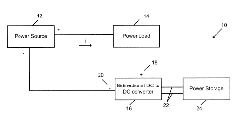
[0029] Fig. 1 schematically illustrates a circuit 10 in which a bi-directional
DC to DC
converter may be used. A power source 12 supplies electrical power to a power
load 14. The
amount of power available in the circuit 10 may not be predictable at all
times. In particular,
power demands of the load 14 may change over time. Additionally, the amount of
energy
available at the power source 12 may not stay constant and may similarly vary
with time. A
bi-directional DC to DC converter 16 may be connected in series with the power
source 12
and load 14. The bidirectional converter 16 may have a positive input terminal
18 and a
negative input terminal 20. Further, the bidirectional converter 16 may have
an output
terminal pair 22.
[0030] In operation, the bidirectional DC to DC converter 16 draws excess
power from the
input terminals 12 and 16 and directs the excess power to a power storage
device 24 via the
output 22. Conversely, when the load 14 requires more power than can be
supplied by the
power supply 12, the bidirectional converter 16 draws power from the power
storage device
24 and outputs the stored power to the circuit 10 via the input terminals 12
and 16.
[0031] The power source may 12 be a battery, a generator, or any other power
source
known in the art. The power load 14 may be a motor, a sensor, or any other
device.
Generally speaking, the circuit 10 may contain various power consuming devices
characterized by different power requirements.
[0032] Referring to Fig. 2, a circuit 50 corresponding to one possible
implementation of
the bidirectional converter 20 may include a positive input terminal 52 and a
negative input
terminal 54. When excess power is available at the input terminals 52 and 54,
a buck PWM
signal 56 may gate power available at the input and direct this power to a
power storage 24
connected to the circuit 50 via the output terminals 58 and 60. At this stage
of the operation
- 6 -
CA 02690050 2009-12-04
WO 2008/157389 PCT/US2008/066968
of the bidirectional converter 16, the voltage across the power storage 24 may
be, for
example, 1V while the voltage across the input terminals 52 and 54 may be 3V.
The "ON"
value of the PWM signal 56 may cause a switch 70 to connect the input 52 to a
positive
terminal 72 of an inductor 74. More specifically, the current may flow from
the terminal 52
through a connection 76 to the terminal 72. A boost PWM signal 80 will
meanwhile remain
in the "OFF' state and will maintain a switch 82 in a disconnected state. The
voltage
difference of 2V (3V -1V), to continue with the example given above, will
apply across the
inductor 74 and will cause the inductor 74 to build up current.
[0033] In the "OFF' state of PWM 56, the switch 70 is in a disconnected state.
The
current may flow through an EMF diode 84 in the direction of the input
terminal 72 of the
inductor 74. The EMF diode 84 may be connected to ground in order to pull
additional
current not supplied at the input and thus increase the overall efficiency of
the circuit 50. As
one skilled in the art will recognize, the current will continue to flow until
the magnetic field
collapses and the electromotive force (EMF) disappears completely. In this
manner, the
energy may transfer to the power storage in a controller manner. In other
words, a higher
voltage available at the input terminals of the circuit 50 is applied in a
PWM, or partial duty
cycle, form to a lower voltage input of a storage device.
[0034] Referring back to Fig. 1, the power load 14 may, at some point, require
more
voltage than the power source 12 may supply. If the power storage 24 stores
enough energy,
the bidirectional DC to DC converter 16 may transfer the necessary power from
the power
storage 24 to the power load 14 and thus enable the circuit 10 to continue
operating.
Referring again to Fig. 2, the voltage across the output terminals 58 and 60
may still be at 1V
while the voltage requirement across the input terminals may 52 and 54 may
remain at or
near 3V. In this state, the buck PWM signal 56 may remain in the "OFF' state
while the
boost PWM signal may not operate the switch 82 to cyclically open and close
the connection.
[0035] In particular, the "ON" state of PWM 80 may close the switch 82. When
the switch
82 is closed, the positive terminal 72 of the inductor 74 will effectively
connect to ground.
This will cause the current to start building up in the inductor 74. When the
PWM 80
transitions to the "OFF' state, the current will flow from the terminal 58 of
the power storage
device 24, through a flyback diode 86, and to the terminal 52. Thus, the
energy saved in the
power storage 24 may be efficiently transferred back to the power load 14.
- 7 -
CA 02690050 2009-12-04
WO 2008/157389 PCT/US2008/066968
[0036] The PWM signals 56 and 80 may operate in accordance with the voltage
sensed
across the terminals 52 and 54 or across the power load 14, for example. In
short, any signal
indicative of the voltage demands in the circuit 10 may be used to regulate
the operation of
the circuit 50 via the PWM signals 56 an 80.
[0037] One skilled in the art will also recognize that an electronic switch
may be a Metal
Oxide Semiconductor Field Effect Transistor (MOSFET), a different type of a
transistor, or
any other high-frequency electronic switching means known in the art.
100381 An exemplary arrangement including a voltage detecting circuit is
illustrated in Fig.
3. A circuit 100 is similar to the circuit 10 with the exception of a voltage
detection circuit
102. The circuit 102 may measure the voltage across the power load 14 and
supply signals
104 and 106 to the bidirectional converter 16. In on possible embodiment, the
signals 104
and 106 may be the PWM signals 56 and 80. Alternatively, the voltage detecting
circuit 102
may not have an oscillation capability and may produce simple voltage signals.
In this case,
the bidirectional converter 16 may drive the PWM pulses 56 and 80 upon
processing the
signals 104 and 106 using additional circuitry (not shown). In yet another
embodiment, the
voltage detection circuit 102 may detect voltage changes across the entire
circuit 100 or, in
other words, across both the power load 14 and the converter 16.
[00391 In one possible implementation, two threshold values may be selected in
view of
the specific requirements of the load 14 or of the entire circuit 100. For
example, the load 14
may generally require 3V to operate but may be still operational anywhere in
the 2.7 ¨ 3.3 V
range. Thus, a voltage detection circuit may be constructed to detect changes
in voltage
across the power load 14 and drive the two PWM signals accordingly. A waveform
120 in
Fig. 4 illustrates an exemplary change of voltage across one or more circuit
elements as a
function of time. As shown, the actual voltage detected by a the circuit 102
may vary in the
2.7 ¨ 3.3 V range while the target voltage in this example may be 3V. The
bidirectional
converter 16 ensures, whenever possible, that the voltage neither exceeds the
upper limit nor
falls below the lower limit. Obviously, excessive voltage may cause damage to
one or more
devices in the circuit 100 while insufficient voltage may prevent the circuit
100 from
operating.
[0040] In reference to Figs. 2 and 4, regions 122 corresponding to the periods
of time when
the detected voltage exceeds the 3V target are associated with the buck mode
of the circuit
- 8 -
CA 02690050 2009-12-04
WO 2008/157389 PCT/US2008/066968
50. As discussed above, in buck mode, the PWM 56 controls the switch 70 in
order to
regulate the transfer of excess power to the storage device 24. On the other
hand, the regions
124 corresponding to the periods of time when the detected voltage falls below
the 3V target
are associated with the transfer of power from the power storage 24 back to
the circuit 10 or
100. In this mode of operation, the PWM 80 drives switch 82 in boost mode.
[0041] Fig. 5 illustrates an exemplary implementation of an analog PWM circuit
adapted
to provide the PWM pulses in response to voltage changes across the terminals
152 and 154.
The terminals 154 and 156 may be connected across the one or more power loads
14 and
possibly across the power source 12 as well. It will be appreciated that the
values of resistors
may be selected according to the specific requirements of the circuit, such as
the range of
tolerable voltages, for example, and according to the type of connection
selected for the
PWM circuit 150. The PWM circuit 150 pulses a small amount of current to
control the
switches 70 and 82. Thus, the two outputs of the circuit 150 are the control
wires 156 and
158. A dotted line 160 is additionally depicted to schematically indicate the
boundary
between the circuits 150 and 50.
[0042] It will be further appreciated here that various other implementations
of the PWM
circuit 150 are possible. For example, the PWM circuit may be implemented by
combining
several available microchips or the entire circuit may be implemented as a
single Application
Specific Integrated Circuit (ASIC).
[0043] It is also contemplated that a microcontroller may be used to generate
the necessary
PWM pulses. As discussed above, a bidirectional DC to DC converter may be used
in for
power scavenging purposes on a 4-20 mA control loop typical in the process
control industry,
for example. In particular, a bidirectional DC to DC converter may be
controlled in such as
manner as to direct excess power available in a 4-20 mA loop to a
supercapacitor, for
example. An additional device, such as a microcontroller-controlled radio, may
be one of the
consumers of this scavenged power. While a PWM circuit 150 could be used to
control the
transfer of power between the radio and the storage device, it may be prudent
to utilize the
microcontroller instead. Because the microcontroller is typically aware of how
much power
the radio requires at a given moment, the microcontroller may generate the PWM
signals 56
and 80 according to these instantaneous demands. In one possible embodiment,
the
microcontroller may direct the bidirectional converter 16 via the boost PWM
signal 80 to
- 9 -
CA 02690050 2009-12-04
WO 2008/157389 PCT/US2008/066968
draw power from the storage device 24 when the radio is transmitting.
Conversely, the
microcontroller may activate the PWM signal 56 when the radio is idle.
[0044] Additionally, the microcontroller may anticipate changes in power
consumption of
the radio by a small amount of time, such as microseconds. For example, the
microcontroller
may direct the bidirectional converter to begin drawing power when a device-
specific
condition requiring power consumption is detected in order to minimize the
delay prior to the
beginning of transmission. More specifically, a sensor operating in a process
control
environment may detect an abnormality such as excessive pressure or
insufficient
temperature, for example, and the microcontroller may effectively prepare the
radio for
transmission by sending a corresponding PWM signal to the bidirectional
controller.
[0045] As yet another alternative, the microprocessor may send simple signals
indicative
of the required voltage while another circuit, either provided as part of the
bidirectional DC to
DC converter or as a separate component, may use this signal to generate the
appropriate
PWM pulses. In this sense, the microprocessor may be programmed with a simpler
logic in
order to allow the radio to retain more of the processing power for radio-
related purposes.
[0046] Of course, the microcontroller may also establish multiple levels of
power demand.
For example, the microcontroller may send wider boost PWM pulses when the
radio is
known to consume large amounts of power in the state of transmission, shorter
boost PWM
pulses when the radio is known to consume moderate power in the state of
reception, and
wide buck PWM pulses when the radio is idle and thus consumes little or no
power.
100471 In another aspect, a bidirectional DC to DC converter may be used in a
circuit
which includes an input-regulated DC to DC converter adapted for scavenging
electrical
power and, in particular, for scavenging power in a circuit characterized by
variable DC
current. Fig. 6 is a schematic representation of a system in which an input-
regulated power
scavenging device may be used to efficiently harvest excess power from a
current loop and
direct the excess power to a load, a storage device, or both. As illustrated
in Fig. 6, a current
loop or circuit 210 includes a Distributed Control System (DCS) 212, a field
device 214, and
a power scavenging device 216 connected in series with the field device 214.
These and
other circuit elements illustrated in Fig. 6 are connected in a wired manner.
- 10-
CA 02690050 2009-12-04
WO 2008/157389 PCT/US2008/066968
[0048] In operation, the DCS 212 and the field device 214 send and receive 4-
20 mA
analog signals in a manner unpredictable to the scavenging device 216
implemented as an
input regulated DC to DC converter. In other words, from the perspective of
the scavenging
device 216, the current in the loop 210 may uncontrollably vary with time in
the 4 to 20 rnA
range. The power scavenging device 216 is connected to the loop 210 in series
through a pair
of input terminals 218, with one of the contacts of the pair 218 connecting
directly to the
positive terminal of the DCS 212 and the other contact connecting directly to
the positive
input of the field device 214. However, the scavenging device 216 may instead
be connected
to the respective negative terminals of the DCS 212 and field device 214.
During operation,
the power scavenging device 216 creates a regulated voltage drop across the
input terminals
218. The scavenging device 216 may maintain the voltage at a constant level
and thus vary
the power consumption at input terminals 218 linearly with the current flowing
through the
scavenging device 216. The scavenging device 216 may then transfer the power
harvested
from the input terminals 218 to one or more devices or circuits connected to
the output of the
scavenging device 216. In another embodiment, the scavenging device 216 may
regulate the
input voltage according to the current flowing through the scavenging device
216. In
particular, the scavenging device 216 may increase the voltage drop across the
input
terminals 218 as the current through the scavenging device 216 decreases.
[0049] A scavenger-powered load 220 may be connected to the power scavenging
device
216 through a pair of output terminals 222. The scavenger load 220 may be any
type of
device consuming either constant or variable power. For example, the scavenger
load 220 be
a simple electrical element characterized by constant power consumption such
as a light
emitting diode (LED), for example, or a complex device with varying power
demands such as
a radio transceiver. It will also be appreciated that while only one scavenger
powered load is
shown in Fig. 6, the power scavenging device 216 may supply power to multiple
loads with
different power consumption characteristics.
[0050] The scavenging device 216 may be also connected to a power storage 224.
The
power storage 224 may be, for example, a single supercapacitor, a relatively
complex
circuitry involving several capacitors connected in parallel, or any other
suitable type of a
power storage, including those known in the art. As one skilled in the art
will recognize, a
capacitor may be used as a power storage device because the voltage across a
capacitor will
- 11 -
CA 02690050 2009-12-04
WO 2008/157389 PCT/US2008/066968
increase as current arrives at the capacitor. A high density capacitor, or a
supercapacitor, is
capable of storing a high amount of charge and may thus be preferable as a
power storage
device.
[0051] Additionally, an adjustable shunt regulator 226 may be connected across
the pair of
output terminals 222 in parallel with the scavenger-powered load 220 and the
power storage
224. The shunt regulator 226 may be used to dissipate the unnecessary power if
the
scavenger-powered load 220 does not consume all the power available at the
output terminals
222. The shunt regulator 226 may be necessary if the power storage 224 is not
provided. In
other embodiments, it may be preferable not to use a shunt regulator in the
loop 210 at all and
save all of the excess power from the output terminals 222 in the power
storage 224. The
adjustable shunt regulator 226 may be implemented in any manner known in the
art such as,
for example, by using a zener diode and one or several resistors.
[0052] As yet another option, a capacitor 228 may be connected across the
output
terminals 222 in order to filter out the output voltage. Because the output of
the power
scavenging device 216 is unregulated, the capacitor 228 may be used to smooth
out the
output voltage particularly if a scavenger powered load 220 is present in the
circuit 210. In
this sense, the capacitor 228 may be part of a post-regulating circuitry.
However, the
capacitor 228 may not be necessary if the power scavenging device 216 supplies
power
primarily to the power storage device 224. In fact, the unregulated aspect of
the output at the
terminals 222 may actually be desirable if the power at the output terminals
222 is transferred
to the power storage 224.
[0053] Meanwhile, an input filter capacitor 230 connected across the input
terminals 218
the power scavenging device 216 may serve to filter out the input noise. As
one skilled in the
art will recognize, an input filter capacitor is needed at the input of any DC
to DC circuit.
The capacitance of the input filter capacitor 230 is a function of the
operating frequency of
the DC to DC converter used in the power scavenging device 216. Additionally,
the voltage
across the input terminals 218 may be clamped in order to prevent a failure in
the scavenging
device 216 from interrupting current flow in the loop 210. For example, a
zener diode 232
may be used to ensure that if the voltage across the input terminals 218 rises
above a certain
limit, the diode will break down and the current will flow in the direction of
the 4-20 mA
- 12 -
CA 02690050 2009-12-04
WO 2008/157389 PCT/US2008/066968
field device 214. One of ordinary skill in the art will recognize that the
limit is determined by
the physical properties of the selected diode.
[0054] The capacitors 228 and 230, the shunt regulator 226, and the zener
diode 232 may
be included in the power scavenging device 216. Depending on the intended
field of
application, the power scavenging device may be adapted to regulate the output
voltage by
means of a shunt circuit 226 or to direct all of the available power to a
power storage device
224. It is contemplated that several configurations, with some of the
components illustrated
in Fig. 6 omitted and some additional components added according to the
desired application,
may be placed into Application Specific Integrated Circuits (ASICs).
Alternatively, the
scavenging device 226 may be provided as a separate ASIC which can then used
in any
configuration discussed herein. As yet another alternative, parts of the
circuitry of the power
scavenging device may be manufactured as a separate chip working in
cooperation with a
conventional DC to DC converter.
[0055] Fig. 7 illustrates the power scavenging device 216 in more detail. In
accordance
with this exemplary layout, the current enters the power scavenging device 216
at the positive
terminal 240 of the input terminal pair 218 and leaves through the negative
terminal 242.
After entering via the positive terminal 240, the current flows to the
positive terminal of the
inductor 244. Additionally a relatively small part of the current flows to the
input regulating
circuit 246. The same or substantially same amount of current that enters
through the
positive terminal 240 leaves through the negative terminal 242. Meanwhile, the
circuitry
implemented according to the teachings of the present disclosure and discussed
in detail
below maintains a regulated drop across the terminals 240 and 242. For
example, the voltage
drop across the terminals 240 and 242 of a scavenging device used in a 4-20 mA
current loop
may be maintained at a constant 1V.
[0056] Referring still to Fig. 7, a boost DC to DC controller 250 regulates
the amount of
time the inductor 244 accumulates current. The controller 250 may be an off-
the-shelf chip
such as On Semiconductor NCP1421 or a circuit assembled from several discrete
IC
components capable of performing a high frequency switching function and to
regulate the
duty cycle of a switched circuit according to a feedback signal. In
particular, the controller
may use one or more Metal Oxide Semiconductor Field Effect Transistors
(MOSFETs), for
example, to quickly open and close electrical connections. The controller
adjusts the timing
- 13 -
CA 02690050 2009-12-04
WO 2008/157389 PCT/US2008/066968
between opening and closing the connections according to the parameters of the
oscillation
circuit components used in the controller and to the feedback signal, such as
current or
voltage. In this sense, the controller 250 may provide Pulse Width Modulation
(PWM) with
a controlled duty cycle to the circuitry of the power scavenging device 216.
It will be
appreciated that the switching functionality can also be implemented by using
discrete
semiconductors, OTS integrated circuits, or other components and materials
known in the art.
[0057] As illustrated in Fig. 7, the controller 250 is equipped with a switch
pin 252, a
feedback pin 254, an output pin 256, and a ground pin 258. It will be
appreciated that the
controller 250 may have additional inputs and is not limited to the four pins
listed above. As
illustrated in Fig. 7, switch pin 252 is electrically connected to the
negative terminal of the
inductor 244, the output pin is connected to one of the output terminals 222,
and the ground
pint 252 is electrically connected to the opposite terminal of the terminal
pair 222 and to the
negative input terminal 242. Further, the feedback pin 254 is connected to the
output of the
input regulating circuit 246.
[0058] During each cycle of operation, the controller 250 first electrically
connects the
input to the switch pin 252 to the ground pin 258. While the pins 252 and 258
are connected,
the current builds up in the inductor 244. Next, the controller 250
disconnects the pins 252
and 258. The collapse of the magnetic field in the inductor 244 pushes the
current from the
inductor 244 to the positive side of the output terminal pair 222. Further,
the negative
terminal of the inductor 244 may be connected both to the switch pin 252 and
to the positive
side of the output terminal pair 222 via a flyback diode 260. The flyback
diode 260 is
preferably a Schottky diode but may also be a different type of a diode. The
flyback diode
260 provides synchronous rectification to the output of the inductor 244.
However, if the
controller 250 is already capable of synchronous rectification, a flyback
diode may not be
required.
[0059] With continued reference to Fig. 7, some of the current entering the
scavenging
device 216 at the terminal 240 is directed to the input voltage regulating
circuit 246. The
circuit 246 may generate a voltage signal indicative of the strength of the
current at the input
terminal 240. The controller 250 uses the signal generated by the regulating
circuit 246 in
order to selectively increase or decrease the production of power at the
output terminal pair
222. For example, the controller 250 may increase the duty cycle of the pulses
and thus
- 14 -
CA 02690050 2009-12-04
WO 2008/157389 PCT/US2008/066968
lower the input voltage across the terminal pair 218 in response to the
voltage level detected
by the circuit 246. The implementation of the circuit 246 is discussed in
greater detail below.
[0060] Fig. 8 illustrates an electrical diagram of one possible embodiment of
a power
scavenging device 270. In this configuration, the power scavenging device 270
incorporates
both a diode 232 to clamp the voltage at a desired level and an input filter
230. Importantly,
in the configuration depicted in Fig. 8, the output voltage is controlled by
the shunt circuit
226. As indicated above, this configuration may be useful if an input
regulated DC to DC
converter is used to power a load requiring a constant voltage. The shunt
circuit 226 will
dissipate the excess power and ensure that the power load does not receive
more power than
is required.
[0061] The input voltage regulating circuit 246 includes an operational
amplifier 272 and
resistors 274 and 276. The amplifier 272 may use the reference voltage 278 at
its non-
inverting input and the variable voltage at its inverting input to control the
relationship
between the input voltage across the terminals 240 and 242 and the voltage
supplied to the
feedback pin 254. One skilled in the art will appreciate that the values of
the resistors 274
and 276 may be selected according to the desired voltage drop. As discussed
above, in a
typical 4-20 mA loop, such as one used in the process control industry, a
voltage drop of 1V
across the scavenging unit 216 or 272 is usually tolerable. Similarly,
resistors 278 and 280
used in the shunt circuit 226 may be selected according to the desired voltage
output.
[0062] Fig. 9 illustrates another contemplated embodiment of an input
regulated DC to
DC converter which can be used for power scavenging. A power scavenging
circuit 290 may
include most of the elements of the power scavenging device 270 discussed
above.
Additionally, the power scavenging circuit 290 may regulate the input voltage
in a more
efficient and practical manner than the scavenging device 270. In particular,
the control loop
210 may experience lower voltage drops across various circuit elements such as
the field
device 214 when the current in the loop 210 is lower. In the case of a 4-20 mA
circuit used in
the process control industry, for example, the DCS 212 will "see" a lower
voltage drop across
the loop when it generates a 4 mA signal and, conversely, the DCS 212 will see
a higher
voltage drop when the analog signal is closer or at the 20 mA level.
Similarly, a field device
such as the device 214 will typically see a lower or higher voltage drop
across the DCS 212
when the field device generates, rather than receives, a 4-20 mA signal. Thus,
the loop 210
- 15-
CA 02690050 2009-12-04
WO 2008/157389 PCT/US2008/066968
may tolerate larger voltage drops across the scavenging circuit 216, 270, or
290 at lower loop
currents.
100631 The power scavenging device 290 illustrated in Fig. 9 draws more power
from the
input terminal pair 218 at lower input currents entering the scavenging device
290 through
the terminal 240 than the scavenging device 270, for example, because the
device 290 drops
more voltage across the terminal pair 218. Clearly, this feature may be
desirable if the
scavenger-powered load 220 has high-power requirements. In particular, a
regulating circuit
291 including the amplifier 272, a gain-limiting component or resistor 292,
and resistors 294-
300 regulates the voltage across the terminal pair 218 so that the input
voltage varies
inversely with the input current as sensed by the circuit 291. The elements
292-300, as well
as the reference voltage 302, are selected and connected in a manner that
generates a larger
feedback signal from the regulating circuit 291 to the feedback pin 254 when
the input
cuiTent is larger. In this sense, the scavenging device 290 utilizes the
negative impedance of
the regulating circuit 291. Thus, in response to a larger signal at the
feedback pin 254, the
controller 250 will reduce the duty cycle of the PWM and thus reduce the
amount of power
pumped to the output terminals 222. Similarly to the power scavenging devices
216 and 270,
the scavenging device 290 regulates the input voltage irrespective of the
output of the
scavenging device 290.
[0064] It will be further appreciated that the inverse relationship between
the input current
voltage supplied to the feedback pin 254 may be implemented by other means
known in the
art. In the embodiment illustrated in Fig. 9, for example, the resistor 300
functions as the
output current sensor because the current returning from the scavenging device
290 to the
output terminal 242 must pass through the resistor 300. However, any known
means of
sensing the current may be similarly used to regulate the feedback pin 254 of
the controller
250 and thus vary the amount of power drawn by the scavenging device 290.
[0065] Generally speaking, it is desirable to select the circuit element
parameters in view
of the maximum tolerable voltage drop. For example, it is prudent to select
the resistance
values of the resistors 292-300 according to the voltage drop tolerable at 20
mA if the
scavenging device 290 is intended for use in a process control industry. Fig.
10 illustrates an
exemplary input and voltage at the input of the power scavenging device 290
connected in a
4-20 mA loop as functions of time. In particular, the waveform 310 may be the
current
- 16-
CA 02690050 2009-12-04
WO 2008/157389
PCT/US2008/066968
flowing through the input terminal 240 while the waveform 320 may be the
voltage across
the input terminal pair 218. Both waveforms are depicted on a relatively large
time scale,
such as seconds. As illustrated in Fig. 10, the inverse relationship between
the input voltage
and the input current ensures that the waveform 220 appears to be a mirror
reflection of the
waveform 310. It will be also appreciated that the waveform 320 may appear as
having a
delay 322 relative to the waveform 310 which may be in the order of micro- or
even
nanoseconds. The scavenging unit 290 maintains the voltage drop within the 1-2
V range as
a function of the input current only and independently from the voltage or
power
requirements at the output terminals 222.
[0066] Another desirable aspect of operation of any scavenging device is
safety and, in
particular, the Intrinsic Safety (I.S.) standards accepted in many industries.
Generally
speaking, I.S. certification associated with a device places specific energy
limitations on this
device. For example, handheld HART communicators are limited to Vo, <= 2V and
Lc <= 32
mA, where V , is the maximum voltage across the communicator and I. is the
maximum
current allowed through the communicator. The I.S. standards associated with a
HART
communicator may be used as a guideline to designing a safe scavenging device
for use in a
4-20 mA because providing power to HART communication circuit is a highly
probable field
of power scavenging application.
[0067] As discussed above, boost DC to DC converters known in the art may draw
too
much power from the input terminals and interfere with the operation of the
circuit from
which the power is being scavenged. This type of interference inay prevent
devices from
receiving power or signals propagated through the circuit. On the hand, the
conventional DC
to DC converters may also fail to contain the scavenged power in a fault
condition and
damage the circuit by releasing the energy back into the circuit, especially
if the scavenged-
powered load is a capacitor or a similar power storage device. This type of
failure may be
more dangerous than overdrawing power from the circuit. If used in the process
control
industry, for example, the conventional boost DC to DC converters may carry a
high
operational risk at least because a 4-20 mA loop may connect explosive or
otherwise
hazardous devices. Thus, sudden spikes in the loop current may cause a spark
thereby
triggering an explosion. However, meeting the safety standards discussed above
by any
- 17 -
CA 02690050 2009-12-04
WO 2008/157389 PCT/US2008/066968
conventional means would inevitably reduce the power efficiency of a boost DC
to DC
converter.
[0068] Because an input regulated transformer consistent with the embodiments
disclosed
herein is particularly well-suited for harvesting power for a power storage
device, meeting the
Intrinsic Safety (I.S.) limitations is clearly a concern in the implementation
of such a
transformer. Fig. 11 illustrates an isolated input regulated DC to DC
transformer 350 used
for power scavenging in current loop 210. The DC to DC transformer or power
scavenging
device 350 provides a fault energy limitation by means of an isolation
transformer 355.
Importantly, the isolation transformer 355 may effectively replace the
inductor 244 in
addition to ensuring operational safety. Meanwhile, the switching circuitry,
such as the
controller 250 working in cooperation with the feedback regulator 246, may
generate PWM
pulses in the same manner as in the embodiment of Fig. 8 irrespective of
whether the power
is supplied to the inductor 244 or the isolation transformer 355. The
transformer coils wired
to a circuit side 357 of the scavenging device 350 may be used to accumulate
electric current
when the switch pin 252 is switched to the ground pin 258 while inducing the
opposite
current in the coils connected to a load side 359. In other words, the
isolation transformer
355 may be regarded as an inductor with an additional function of an
electrostatic shield.
[0069] Referring back to Fig. 8, there is a direct discharge path from the
output 222 back to
the input 218 in a fault condition caused by the shorting of the flyback diode
260.
Additionally, the internal circuitry of the controller 250 may similarly
create a virtually
resistance-free path between the output 222 and the input 218. By contrast,
the isolation
transformer 355 in the embodiment illustrated in Fig. 11 prevents the energy
from being
transferred back to the input 218. As one skilled in the art will recognize,
an isolation
transformer may be considered fail-safe for all practical purposes as long as
the proper
transformer with the corresponding core saturation characteristics is
selected.
[0070] Further, the coil ratio of the isolation transformer 355 may be
selected to
additionally provide a voltage transformation desirable in certain
applications. Thus, rather
than using additional circuitry to regulate the voltage supplied to the power
load, the isolation
transformer 355 may provide an efficient means of controlling the output
voltage. Moreover,
a transformer may be constructed with multiple windings in order to provide
multiple
outputs, if required in a particular application.
- 18 -
CA 02690050 2009-12-04
WO 2008/157389 PCT/US2008/066968
[00711 It will be further recognized that it may not be necessary to maintain
absolute
isolation between the supply circuit side 357 and the load side 359. In
particular, feedback
voltage or power signals may be supplied from the load side 359 to the supply
side 357 for
reference or additional regulating purposes as long as the connections across
the isolation
boundary include adequately sized infallible resistors. Also, it may be
necessary to limit the
power transferred through the transformer in the forward direction, or in the
direction from
the supply side 357 to the load side 359. These limitations can help achieve
the desired limits
on the power transfer in the opposite direction. Although elements performing
these
functions are not shown in Fig. 11, it will be noted here that these forward
limitations may be
achieved by a shunt regulator connected at the input to the transformer on the
supply side
357.
[0072] With continued reference to Fig. 11, clamp diodes 362 may be
additionally
connected across the input terminals 218 to limit the voltage at the input of
the power
scavenging device 350 in order to establish a maximum voltage in fault
conditions for I.S.
purposes. One skilled in the art will recognize that the clamp diodes 362 have
no effect on
the scavenging device 350 in normal operating modes of the device 350.
[0073] Fig. 12 illustrates another embodiment of a power scavenging device
using an input
regulated DC to DC converter. Here, a current loop 400 includes a HART
communicator 402
in addition to the DCS 212 and the field device 214 discussed above in
reference to Fig. 6.
The HART modulator 402 is connected across in parallel with the field device
214 in order to
modulate voltage across the field device. As is known in the art, the ability
to modulate
voltage across a circuit depends on the impedance of the circuit. In
particular, low
impedance of the circuit requires a modulating circuit to spend a large amount
of energy.
Meanwhile, the DCS 212 could be a battery with a very low impedance and thus a
typical 4-
20 mA current loop is not conducive to HART communications. It is therefore
desirable to
increase the impedance of the loop 400. Moreover, it is desirable to meet this
objective
without using such conventional means as an inductor because an inductor would
shunt the
usable power. Thus, while it may be possible to increase the impedance of the
loop 400 with
an inductor, it may not be possible to scavenge enough power from the loop 400
in order to
power the HART communication circuit 402.
- 19-
CA 02690050 2009-12-04
WO 2008/157389 PCT/US2008/066968
[0074] In accordance with an embodiment illustrated below, the power
scavenging device
216, in addition to providing power to the load 220, appears as a virtual
inductor 404
connected in series with the field device 214. The virtual inductor 404 is not
a physical
device separate from the power scavenging device 216. Rather, a particular
embodiment of
the scavenging device 214 presents the device 214 to the circuit 400 as an
inductor so that the
HART communicating circuit 402 may modulate signals over the wires of the
circuit 400.
Additionally, a capacitor 406 provides a filtering function in order to smooth
out the sudden
changes in current which may interfere with HART communications.
[0075] A power scavenging device 450 schematically illustrated in Fig. 13
operates in
such a way as to control the rate of change of current through the power
scavenging device
450 thereby creating AC impedance. Additionally, the power scavenging device
450 reduces
the noise level and ensures that the circuit 400 is conducive to voltage
modulation and, in
particular, to HART communications. As illustrated in Fig. 13, the power
scavenging device
may power a HART communication circuit 452 and may, in this particular
embodiment,
include the HART communication circuit 452 as an integral component.
[0076] As illustrated in Fig. 13, the capacitor 406 is connected in parallel
with the field
device 214 in order to filter out the loop noise. However, the capacitor 406
need not be part
of the scavenging device 450 and may be provided separately, as illustrated in
Fig. 12.
Additionally, an input noise filter 454 is connected in series with the DCS
212 and the field
device 214. Similarly to other embodiments discussed herein, the selection of
the input noise
filter 454 is a function of the operating frequency of the controller 250 as
well as of the
allowable noise amplitude at the input terminals 218. For example, a 1 F
capacitor may be
used as the input filter 454 in a 4-20 mA circuit loop with the allowable
voltage drop of -1V
and the voltage output to a scavenger load of -3V. One skilled in the art will
appreciate,
however, that the input filter 454 in this and other embodiments may also be
considerable
larger.
[0077] The feedback circuit 455 functions in a manner largely similar to the
operation of
the feedback circuit 246 illustrated in Fig. 8. However, the feedback circuit
455 additionally
includes a capacitor 456, effectively coupling a signal indicative of the
current entering the
scavenging device 450 to the inverting input of the amplifier 272. This
configuration
provides a dynamic characteristic of limiting the rate of change of a current
458 through the
- 20 -
CA 02690050 2009-12-04
WO 2008/157389 PCT/US2008/066968
scavenging device 450 and into the field device 214. Additionally, the
combination of the
energy storage in the capacitor 406 and the limited rate of change of current
through the
scavenging device 450 provides the filtering function which can isolate the
communication of
the HART communication circuit 452. The limited rate of change of the current
458 through
the scavenging device 450 additionally functions as a series impedance for the
loop current.
[0078] The power scavenging device 450 may be further improved by clamping the
voltage at the input terminals of the device 450 by means of a breakdown
diode, for example.
Moreover, an isolation transformer similar to the transformer 355 illustrated
in Fig. 11 may
be used in place of the inductor 244 to provide I.S. energy limiting. The
isolation transformer
used in place of the inductor 244 may further include a coil configuration
suitable for
adjusting the output voltage. One skilled in the art will appreciate that
various aspects of the
embodiments illustrated in Figs. 6-13 may be combined to achieve various
application goals.
[0079] Additionally, the scavenging device 450 may provide multiple outputs
and may
maintain each output voltage at a different level by using shunt regulators,
for example. Fig.
13 illustrates a typical configuration of the shunt regulator 226 which
dissipates excess power
provided to a power load connected to an output terminal pair 460. Because an
input
regulated DC to DC converter harvests the available power at a given input and
at a regulated
voltage drop, additional voltage regulators may be required to provide
regulated voltage to
scavenger-powered loads. It is contemplated that the embodiment illustrated in
Fig. 13 may
provide power to a radio transceiver as well to as to a HART communication
circuit.
Additionally, the excess power may be stored in a power storage device, such
as the device
224, instead of being dissipated by a shunt regulator.
[0080] It is further contemplated that the filter function of the scavenging
device 450 may
be selectable. By being able to turn off the filtering functionality when it
is not required,
users of the device may find additional applications for a scavenging device
discussed herein.
[0081] Thus, as discussed above, the input-regulated DC to DC converter of at
least some
of the embodiments maintains a substantially constant voltage drop across the
input terminals
and directs the power available at the controlled voltage drop to a pair of
output terminals.
Depending on the characteristics of the circuit including such input-regulated
DC to DC
converter, the voltage at the output terminals of the input-regulated DC to DC
converter may
-21-
CA 02690050 2009-12-04
WO 2008/157389 PCT/US2008/066968
vary during operation and, in some applications, the variation may not be
predictable to a
load powered by the input-regulated DC to DC converter.
[0082] As one example, Fig. 14 schematically illustrates a circuit 500 in
which a
bidirectional converter 502 regulates power transfer between a storage device
504 and a
constant-voltage load 506 powered by an input-regulated power scavenging
device 510
producing unregulated voltage across a pair of output terminals 512. In this
example, the
circuit 500 includes a 4-20 mA control loop in which a DCS 520 and a field
device 524
communicate via 4-20 mA signals. The input-regulated power scavenging device
510 is
connected in series with the field device 524 to form a current loop 530
including the DCS
520, the field device 524, and the power scavenging device 510. In operation,
the power
scavenging device 510 harvests excess power available in the current loop 530
while
regulating the voltage drop across the input terminals of the power scavenging
device 510. In
some embodiments, the power scavenging device 210 may maintain a substantially
constant
voltage drop in order not to disrupt signaling in the loop 530. Because the
current in the loop
530 may vary in the 4-20 mA range, the power scavenging device 510 may draw
variable
amounts of power available in the loop 530 and provide the available power at
a non-constant
voltage at the output terminals 512. However, the load 506 powered by the
scavenging
device 510 may require constant voltage to operate. While it may be possible
to connect the
output terminals 512 of the power scavenging device 510 to an adjustable shunt
regulator to
dissipate excess power and thereby maintain a constant voltage for a power
scavenger-
powered load 506, shunt regulators and other means of disposing of extra
energy clearly lack
efficiency.
[0083] On the other hand, the bidirectional DC to DC converter 502 connected
in series
with the output terminals 512 of the input-regulated power scavenging device
510 and with
the load 506 may, at different stages of operation, either efficiently harvest
power when
excess power is available in a loop 540 (defined by at least the three modules
502, 506, and
510), or compensate for power deficiencies in the loop 540 by redirecting
power from the
power storage 504 to the load 506. To this end, the bidirectional DC to DC
converter 502
may operate in a manner similar to the operation of the bidirectional DC to DC
converter 16
discussed above, for example.
- 22 -
CA 02690050 2013-09-04
100841 Additionally, a voltage detection circuit 542 may control the operation
of the
bidirectional DC to DC converter 502 by measuring the voltage drop across the
load 506 and
accordingly supplying control signals to the bidirectional DC to DC converter
502 via control
lines 544 and 546. In some embodiments, the voltage detection circuit 542 may
be similar to
the circuit 102 discussed above with reference to Fig. 3. Alternatively, the
voltage detection
circuit 542 may be integral to the load 506 so that the load 506 may
effectively control the
direction and amount (e.g., as PW'M timing) of power transfer through the
bidirectional DC
to DC converter 502. In either case, the bidirectional DC to DC converter 502
may transfer
power to the power storage 504 when the voltage detection circuit 542 reports
a voltage drop
in excess of a certain high threshold and, conversely, from the power storage
504 when the
voltage detection circuit 542 reports a voltage drop below a certain low
threshold.
[0085] Referring to Fig. 15, a circuit 550 is similar to the circuit 500
discussed above.
However, rather than relying on the voltage detection circuit 542, the circuit
550 includes an
intelligent controller 552 which communicates with the load 506 and regulates,
via control
lines 544 and 546, the direction and amount of power transfer through the
bidirectional DC to
DC converter 502. In one embodiment, the intelligent controller 552 and the
load may
communicate via a standard RS-232 connection to exchange messages according to
an
appropriate communication protocol. By processing messages from the load 506,
the
controller 552 may increase or decrease the width of PWM pulses, reverse the
direction of
power transfer, and otherwise regulate the circuit 540 via the control lines
544 and 546.
[0086] It will be appreciated that the circuit 550 may optionally include a
voltage detection
circuit 542 which may report voltage measurements to the controller 552, for
example.
Further, it is contemplated that some of the components discussed above may be
combined to
simplify housing and packaging, for example. In one such contemplated
embodiment, a
bidirectional DC to DC converter 16 or 502 may include a supercapacitor or
another type of
power storage unit.
[0087] While the present invention has been described with reference to
specific examples,
which are intended to be illustrative only and not to be limiting of the
invention, it will be
apparent to those of ordinary skill in the art that changes, additions and/or
deletions may be
made to the disclosed embodiments, and therefore the claims should be given
the broadest
interpretation consistent with the description as a whole.
-23 -