Note: Descriptions are shown in the official language in which they were submitted.
CA 02690063 2009-12-07
WO 2009/030319 PCT/EP2008/006275
A WAVE CHOKE SYSTEM FOR A MICROWAVE OVEN DOOR
Description
The present invention relates to a wave choke system for an oven door of a
microwave oven. Further, the present invention relates to an oven door of a
microwave oven. Additionally, the present invention relates to a microwave
oven.
A microwave oven generates strong electromagnetic fields in order to heat
the food stuff. Said electromagnetic fields are potential threat to the health
of the operator, if the electromagnetic fields or parts of them leave the cav-
it . '' h., ~ a,,~-,,L .. o' i,i_
y u~ ~e microwave oven is critical. In particular, the microwaves
may leave the cavity through the gap between the door and the cavity.
The gap between the door and the cavity is sealed with respect to micro-
waves by integrating wave chokes into the door of the microwave oven. Said
wave chokes provide a small band stop by a cascaded X/4-transformation.
However, mechanical tolerances of the oven cavity frame and the frame of
the oven door can evoke local areas of an increased leakage.
It is an object of the present invention to provide a wave choke system for a
microwave oven door, which is more robust against mechanical tolerances of
the oven cavity walls and the oven door frame.
This object is achieved by the wave choke system according to claim 1.
According to the present invention the wave trap is subdivided into a plural-
ity of open cells by separating elements on at least one circumferential side
of the oven door, so that the open cells are arranged serially along the longi-
tudinal axis of the wave trap, wherein said separating elements are formed as
a sheet made of a conductive material.
CONFIRMATION COPY
CA 02690063 2009-12-07
WO 2009/030319 PCT/EP2008/006275
2
The main idea of the invention is the wave trap with the separating elements
and the resulting open cells. The open cells are small cavities with one open
side. The open cells allow that the deepness of the wave trap may be in-
creased compared to the prior art. The greater deepness effect that the wave
choke system is more robust against mechanical tolerances.
According to the preferred embodiment of the present invention the dis-
tance between two neighbouring separating elements is greater than the half
of the effective wavelength inside the single open cell related to an
operating
frequency of the microwave oven. This guarantees the effect of the inven-
tion.
Preferably, the distances between neighbouring separating elements are
equal. The equal distances between neighbouring separating elements allow a
simple and an automatic manufacturing of the wave trap.
Alternatively, the distances between neighbouring separating elements may
be are different. In general, it is not necessary, that the distances between
neighbouring separating elements are uniform.
The separating element may be formed as a sheet made of conductive mate-
rial, in particular of metal or a sheet made of dielectric material with metal
coating. Alternatively, the separating element may be formed as a grid made
of metal wires.
According to the preferred embodiment of the present invention the dis-
tances between the neighbouring separating elements are between 30 mm
and 120 mm.
Preferably, the wave trap encloses completely the oven door along the
circumferential direction.
The wave trap is made of metal or a dielectric material coated with metal.
CA 02690063 2009-12-07
WO 2009/030319 PCT/EP2008/006275
3
Further, the wave trap has substantially a rectangular cross section, which
may be bordered by an outer circumferential side, an inner circumferential
side, an outer side and an inner side.
For example, the outer circumferential side, the inner circumferential side
and the outer side form a U-shaped profile. Thus, the wave trap may be used
as a door frame or a part of the door frame.
An open portion of the open channel may be arranged on the inner side of
the wave trap. The inner side comprises a plurality of lamellae. Further, a
gap is arranged between the lamellae and an inner edge of the outer side of
the wave trap. Preferably, the gap has a width between 10 mm and 14 mm.
The separating elements may be rectangular sheets. Thus, the lamellae may
fill a part of the cross section of the wave trap.
The open cells are at least partially filled with at least one dielectric
material.
Additionally or alternatively, the open cells are at least partially filled
with
air.
Further, the present invention relates to an oven door for a microwave oven
comprising the wave choke system as described above.
At last, the present invention relates to a microwave oven comprising the
wave choke system and/or the oven door as described above.
The novel and inventive features believed to be the characteristic of the pre-
sent invention are set forth in the appended claims.
The invention will be described in further detail with reference to the draw-
ing, in which
CA 02690063 2009-12-07
WO 2009/030319 PCT/EP2008/006275
4
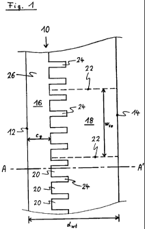
FIG 1 illustrates a schematic partial view of a wave choke system for
microwave oven door according to a preferred embodiment of the
present invention, and
FIG 2 illustrates a schematic sectional view of a part of the oven door
with the wave choke system according to the preferred embodi-
ment of the present invention.
FIG 1 illustrates a schematic partial view of a wave choke system for a mi-
crowave oven door according to a preferred embodiment of the present in-
vention. The wave choke system comprises a wave trap 10. The wave trap 10
is formed as a channel with a rectangular cross section. The wave trap 10
forms a frame or the part of the frame of an oven door of a microwave
oven. Thus, the wave trap 10 forms the outer portion of the microwave oven
door.
The wave trap 10 includes an outer circumferential side 12, an inner circum-
ferential side 14, an outer side 16 and an inner side 18. The outer side 16 is
a
part of the outer side of the oven door. In the same way the inner side 18 is
a part of the inner side of the oven door. The outer circumferential side 12
corresponds with a circumferential side of the oven door or with a part of
said circumferential side. The inner circumferential side 14 encloses at least
partially an inner portion of the oven door. Said inner portion may be a win-
dow, for example.
The inner side 18 comprises a plurality of lamellae 20. Said lamellae 20 ex-
tend into the direction of the outer circumferential side 12. The outer
circumferential side 12, the inner circumferential side 14 and the inner side
16 form a U-shaped profile. Said U-shaped profile is substantially symmetric.
The inner side 16 is smaller than the outer side 18. The inner edge of the
inner side 18 joins the inner edge of the inner circumferential side 14, so
that there is a gap between the inner edge of the outer circumferential side
12 and the outer edge of the inner circumferential side 14. In other words
CA 02690063 2009-12-07
WO 2009/030319 PCT/EP2008/006275
there is a gap 26 between the inner edge of the outer circumferential side 12
and the lamellae 20. In this example the width cg width of the gap 26 is
about between 10 mm and 14 mm. The gap 26 and the slots between the la-
mellae 20 define the open portion of the wave trap 10.
5
The wave trap 10 is subdivided into a plurality of open cells 24 by separating
elements 22. The separating elements 22 are formed as rectangular sheets
made of a conductive material. For example, the separating element 22 may
be a metal sheet. Further, the separating element 22 may be a web made of
metal wire. In this example the distance ws, between two neighbouring sepa-
rating elements 22 is about between 30 mm and 120 mm. The distance ws,
between two neighbouring separating elements 22 must be more than a half
of the =wavclcngt1-1 of iiie inicrowave.
The open cells 24 between the separating elements 22 allow that the deep-
ness d,,t of the wave trap 10 is independent of the wavelength of the micro-
wave. Thus, the deepness d, of the inventive wave trap 10 may be greater
than the deepness of a wave trap according to the prior art. The greater
deepness d,,t of the inventive wave trap 10 effects that the wave choke sys-
tem is more robust against mechanical tolerances of the oven cavity wall.
This results in a reduced leakage of the oven cavity.
FIG 2 illustrates a sectional view of the inventive wave trap 10 along the
line
A-A' in FIG 1. The outer circumferential side 12, the inner circumferential
side 14 and the outer side 16 form the U-shaped profile. In the preferred
embodiment the outer edges of the separating elements 22 are flush with the
edges of the lamellae 20. In general, the depth ds, of the separating elements
22 is arbitrary. The height hw, of the wave trap 10 corresponds with the
height of the separating elements 22.
The space between two neighbouring separating elements 22 forms the open
cell 24. Preferably, the distances ws, between the neighbouring separating
CA 02690063 2009-12-07
WO 2009/030319 PCT/EP2008/006275
6
elements 22 are uniform. However, different distances w5e between the
neighbouring separating elements 22 are also possible.
The inner space of the wave trap 10 may be filled by air or an arbitrary di-
electric material.
The wave choke system according to the present invention allows a reduced
leakage and can be manufactured in a simple way.
Although illustrative embodiments of the present invention have been de-
scribed herein with reference to the accompanying drawing, it is to be un-
derstood that the present invention is not limited to those precise embodi-
.:.ents antu LllaC various other changes and modifications may be affected
therein by one skilled in the art without departing from the scope or spirit
of
the invention. All such changes and modifications are intended to be in-
cluded within the scope of the invention as defined by the appended claims.
CA 02690063 2009-12-07
WO 2009/030319 PCT/EP2008/006275
7
List of reference numerals
wave trap
12 outer circumferential side
5 14 inner circumferential side
16 outer side
18 inner side
lamella
22 separating element
10 24 open cell
26 gap
cg width of the gap
wse distance between separating element
dw, deepness of the wave trap
15 ds, deepness of the separating element
hwt height of the wave trap