Note: Descriptions are shown in the official language in which they were submitted.
CA 02690094 2009-12-04
WO 2008/149125 PCT/GB2008/001982
TITLE
A method for analysing the structure of an electrically conductive object.
FIELD OF THE INVENTION
Embodiments of the present invention relate to a method for analysing the
structure of an electrically conductive object.
BACKGROUND TO THE: INVENTION
Electrical impedance tomography (EIT) is a known imaging technique,
particularly used in medical and other applications for the detection of
underlying morphology. Typically, a plurality of electrodes is attached to an
object to be imaged. Either input voltages are applied across a subset of
'input' electrodes and output electric currents are measured at `output'
electrodes, or input electric currents are applied between a subset of 'input'
electrodes and output voltages are measured at `output' electrodes or
between pairs of output electrodes. For example, when a very small
alternating electric current is applied between a subset of `input'
electrodes,
the potential difference between output electrodes or between pairs of
'output'
electrodes is measured. The current is then applied between a different
subset of 'input' electrodes and the potential difference between the output
electrodes or between pairs of `output' electrodes is measured. An electrical
impedance image based on variations in electrical impedance can then be
constructed using an appropriate image reconstruction technique.
However, the variations of electrical impedance between regions of different
morphology may be too small to be discernible.
One approach to this problem has been to perform EIT over a broad range of
frequencies. Different morphologies that have an insignificant impedance
CONFIRMATION COPY
CA 02690094 2009-12-04
WO 2008/149125 PCT/GB2008/001982
2
difference at one frequency may have a more significant difference at a
different frequency. However, even using different frequencies the variations
of electrical impedance between portions of different morphology may be too
small to be discernible.
It is therefore desirable to be able to better differentiate between different
morphologies using EIT.
BRIEF DESCRIPTION OF THE INVENTION
According to one embodiment of the invention there is provided a method for
analysing the structure of an electrically conductive object, the method
comprising the steps of:
(i) obtaining electrical impedance data for the object;
(ii) analysing the obtained electrical impedance data using a transfer
function of an assumed electrical model to determine a plurality of
electrical impedance properties for the object; and
(iii) imaging one or more of the determined electrical impedance
properties.
Electrical impedance properties, which are related to the measured electrical
impedance data, can be derived from the measured electrical impedance
data, and these electrical impedance properties can be used to analyze the
structure of the object. However, the amount of variation of the individual
electrical impedance properties may be insufficient to enable accurate
analysis.
According to one embodiment of the invention there is provided a method for
analysing the structure of an electrically conductive object, the method
comprising the steps of:
CONFIRMATION COPY
CA 02690094 2009-12-04
WO 2008/149125 PCT/GB2008/001982
3
(i) obtaining electrical impedance data for the object over a range of
frequencies;
(ii) analysing the obtained electrical impedance data using a transfer
function of an assumed electrical model to determine a plurality of
electrical impedance properties for the object;
(iii) constructively. combining seiected ones of the determined plurality of
electrical impedance properties to provide at least one parametric
impedance value for the object; and
(iii) imaging one or more of the determined parametric impedance values.
According to one embodiment of the invention there is provided a method for
analysing the structure of an electrically conductive object, the method
comprising the steps of:
(i) obtaining electrical impedance data for the object
(ii) analysing the obtained electrical impedance data to determine a
plurality of electrical impedance properties for the object;
(iii) constructively combining selected electrical impedance properties from
said plurality of electrical impedance properties to provide parametric
impedance values for the object.
The electrical impedance data for the object may be collected with a
frequency bandwidth of between 0 and 100MHz for biological materials and
up to 100GHz for non-biological conducting materials.
The method may comprise the further step of:
(iv) displaying the parametric impedance values as part of an image from a
region of interest (RIO).
Step (iii) may comprise combining predetermined electrical impedance
properties according to an impedance emphasising algorithm.
CONFIRMATION COPY
CA 02690094 2009-12-04
WO 2008/149125 PCT/GB2008/001982
4
Step (i) may comprise obtaining electrical impedance data for the object at a
plurality of frequencies that depend on the object (bio or non-bio materials).
For biological materials it should transfer function is given by the Cole-Cole
formula [Cole,1920; Cole, 1924] over the frequency range 0-100MHz.
The method may be used to analyse an electrically conductive object having a
cellular structure or cell-like structure, and step (ii) may comprise the use
of
an equivalent electrical impedance circuit to model the structure, such as
Cole-Cole model [Cole, 1920; Cole, 1924]
The equivalent electrical impedance circuit may in the limiting case comprise
a cell membrane capacitance (C), an intracellular resistance (Ri), and an
extracellular resistance (Re).
The electrical impedance properties may be selected from the group
consisting of R; (cell/Group intra resistance), Re (Cell/Group extra
resistance),
C (Cell/Group capacitance), fr (cell/group relaxation frequency) and a
(cell/group relaxation factor).
Step (iii) may comprise combining fr (relaxation frequency) and C (cell/group
capacitance) by multiplication which may provide parametric impedance
values.
BRIEF DESCRIPTION OF THE DRAWINGS
For a better understanding of the present invention reference will now be
made by way of example only to the accompanying drawings in which:
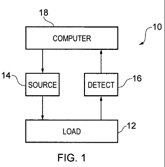
Fig. 1 is a diagrammatic illustration of electrical impedance tomography
apparatus;
Figs. 2A and 2B show graphs of measured electrical impedance as a function
of frequency with single or multiple dispersion;
CONFIRMATION COPY
CA 02690094 2009-12-04
WO 2008/149125 PCT/GB2008/001982
Fig. 3 shows an example electrical impedance circuit model of an object
having a cellular or cellular-like structure at the "micro-scale"; and
Fig. 4 shows a generic electrical impedance circuit model of an object having
a cellular or cellular-like structure at a "macro-scale".
5
DETAILED DESCRIPTION OF EMBODIMENTS OF THE INVENTION
Fig. 1 illustrates diagrammatically electrical impedance measurement or
electrical impedance tomography (EIT) apparatus 10 for measuring
impedance data for a load 12. The load 12 comprises an electrically
conductive object to which are attached a plurality of electrodes. The term
`electrically conductive' means that the object is capable of conducting an
electric current but it does not necessarily need to conduct current very
well.
The apparatus 10 further comprises a signal source 14, a signal detector 16
and a computer 18. In one embodiment, the signal source provides, as an
input signal, an electric current and the signal detector detects, as an
output
signal, voltage. In another embodiment, the signal source provides, as an
input signal, a voltage and the signal detector detects, as an output signal,
electric current.
The computer typically comprises at least a processor and a memory. The
memory stores a computer program which when loaded into the processor
controls the computer.
The input signal is applied using the source 14 to the object via electrodes
and the resulting output signals present at same or other electrodes are
measured using the detector 16. This process is repeated for different
frequencies of input signal. For example, the electric signal may be applied
by
the signal source 14 at a number of frequencies between 0 Hz (direct current)
and 100 MHz, to enable frequency dependent electrical impedance data to be
obtained for the object.
CONFIRMATION COPY
CA 02690094 2009-12-04
WO 2008/149125 PCT/GB2008/001982
6
The separation of the electrodes used for the impedance measurements
determines the resolution or scale at which the object is analysed. The
electrical impedance measurements may be obtained at an expected scale of
interest (e.g. micro-meter or millimeter range). As an example of the scale of
interest, for a biological object, we may be interested in the single cell or
in the
group cell level or at tissue or histology level, such as lobule or duct in
breast
tissue. Subsequently the obtained electrical impedance data will be analysed
using a transfer function of an assumed electrical model to determine a
plurality of electrical impedance properties for the object. The electrical
model
used may depend upon the resolution/scale of the impedance measurements.
Referring to Figs. 2A and 2B, the electrical impedance data obtained using
the above method can be plotted as a function of frequency. This plot 22
represents the impedance changes vs frequencies or transfer function for the
object. The computer 18 is operable to execute an appropriate algorithm to
analyse the obtained impedance transfer function or frequency dependent
impedance properties and thereby determine a plurality of electrical
impedance properties for the object. The electrical impedance properties
typically include one or more of:
a) the impedance at the limit w -> 0 (lower limit)
b) the impedance at the limit w->- (upper limit)
c) (i) the relaxation frequency at which there is a change in the
impedance
(ii) the impedance at that change frequency
(iii) the gradient of the change of impedance, particularly at the
relaxation frequencies;
For example, if there are N dispersions including the Alpha, Beta and Gamma
dispersions of biological materials [Cole K S, Permeability and impermeability
of cell membranes for ions. Cold Spring Harbor Symp. Quant. Biol. 8 pp110-
22, 1940] within the frequency range used, where N>1, then the dispersion
CONFIRMATION COPY
CA 02690094 2009-12-04
WO 2008/149125 PCT/GB2008/001982
7
frequencies w1, w2, ...WN_1, WN, are identified and the electrical impedance
properties for a particular dispersion m would typically include one or more
of:
a) For m=1, the impedance at the lower (global) limit w -> 0
For m>1, the impedance at the lower (local) limit w -> wm- a, where a<(
Wm - Wm_1) and may possibly be'/( wm - wm_1)
b) For m=N, the impedance at the upper (global) limit w->-
For m<N, the impedance at the upper (local) limit w-> wm + b, where b<(
Wm+1 - Wm) and may possibly be b - '/z( Wm+1 - wm)
c) (i) the relaxation frequency wm (f,) at which there is a change in the
impedance
(ii) the impedance at that change frequency
(iii) the gradient of the change
The amount of variation of one or more of these impedance properties can be
used to analyse the structure of the object due to the intra/extra cellular or
intra/extra cellular-like related changes.
In some embodiments, the object under analysis is modeled using an
equivalent electrical impedance circuit. The object may be modeled using an
equivalent electrical impedance circuit 20 illustrated in Fig. 3. Objects
which
may be modeled using the equivalent electrical impedance circuit 20 may, in a
non-limiting example, include human or animal tissue, and porous or other
cellular or cellular-like materials.
In the illustrated embodiment, the equivalent electrical impedance circuit 20
comprises a cell portion 21 in parallel with an extra-cell portion 23. The
cell
portion 21 has a capacitance C and a resistance Ri in series. The resistance
C is associated with the cell membrane/boundary and the resistance R;, is
associated with the interior of the cell. The extra-cell portion 23 has a
resistance Re . The resistance Re is associated with the structure outside the
cell. The resistance Re is connected in parallel with the series connected
capacitance C and resistance Ri.
CONFIRMATION COPY
CA 02690094 2009-12-04
WO 2008/149125 PCT/GB2008/001982
8
A non-limiting example of a single dispersion impedance transfer function for
this circuit is:
Z(w) __ Re (1 + j.cv.C.Ri )
1+ j.cv.C.(Re+Ri)
In the limit w-> 0, Z-> Re
In the limit w->-o, Z-> R;// Re i.e. R; Re/( R;+Re)
There is a change (dispersion) at frequency fr and an impedance Zr that has a
gradient a.
The transfer model for multiple dispersion in biological tissue can be modeled
by the Cole-Cole equation (Cole K S 1940, Cole K S 1941, McAdams E T et
al, 1995) as follows:
Z=ROc +(RO-ROc)/(1 +(jf/fr))(1-a)
Usually this equation can be rewritten as the equation below if a three-
element electrical equivalent circuit is used for a simple modeling cell
suspensions (Fricke and Morse, 1925) or tissues:
Z=Re= Ri/(Re+Ri)+(Re-Re= Ri/(Re-f'Ri))/(1 + (jf/ fr) )(1-a)
Where Roc is the result of paralleling Re and Ri.
There are changes (dispersion) at frequency f~; and impedance Z,; that has a
gradient a;.
CONFIRMATION COPY
CA 02690094 2009-12-04
WO 2008/149125 PCT/GB2008/001982
9
.As indicated above, the computer 18 is operable to execute an appropriate
algorithm to analyse the measured impedance data and extract a plurality of
electrical impedance properties for the object under analysis. For example,
based on the measured impedance data, the algorithm may be operable to
plot impedance data points as a function of frequency and produce a best fit
line 22 using the model to form the transfer function illustrated in Fig. 2.
From
this transfer function, the computer 18 is capable of determining a plurality
of
individual impedance properties for the object. These impedance properties
may include:
a) the impedance at the limit w -> 0, which gives Re
b) the impedance at the limit w->-, which gives R; Re/( Ri+ Re)
c) (i) the relaxation frequency fr at which there is a change in the
impedance
(ii) the impedance Zr of the transfer function at that change frequency
(iii) the gradient a of the change which gives the relaxation factor.
The impedance properties may be used to determine further impedance
properties using the model.
For example, if both Re and R; Re/( Ri + R.) are known then Ri can be
determined.
The impedance Zr of the transfer function at the change (dispersion)
frequency fr, is where the capacitor dominates the transfer characteristic as
with each small increases in frequency it conducts significantly better
reducing
the impedance. The impedance Zr at the change (dispersion) frequency fr,
can be modelled as 1/0.2;r f,.C). Therefore C can be determined as 1/(j.2,v
fr.
Zr).
CONFIRMATION COPY
CA 02690094 2009-12-04
WO 2008/149125 PCT/GB2008/001982
Variations of the individual impedance properties (Re, Ri, fr, Zr, a, C) may
be
used to analyse the structure of an object. For example, in the case of human
tissue, variations in the individual impedance properties may be indicative of
the presence of an abnormality as this gives rise to electrical
characteristics
5 which are different to those exhibited by normal, healthy tissue.
However, the amount of variation of the individual impedance properties may
be insufficient to enable accurate analysis of the structure. For example, the
amount of variation of cell membrane capacitance (C) or relaxation frequency
10 (fr) may be insufficient to be readily detectable, for example in images of
the
object constructed based on those individual impedance properties.
In embodiments of the invention, selected predetermined impedance
properties are `constructively' combined to provide a parametric impedance
value for the object. Constructive combination of the impedance properties in
this way to provide parametric impedance value emphasises the variation of
the individual electrical impedance properties. This enables the structure of
the object to be more accurately analyzed. The parametric impedance value
at a particular position may be represented as a pixel value at a
corresponding position in an image of the object.
Taking a simple example, if there is a 10% increase in one of the electrical
impedance properties, such as cell membrane capacitance (C) from an initial
value C, to 1.1 CI, and a 10% increase in another of the electrical impedance
properties, such as relaxation frequency (fr) from an initial value frl to
1.1frJ,
these individual 10% increases may be insufficient to be readily detectable,
for example discernable in images based on these individual electrical
impedarice properties. However, combination of these individual electrical
impedance properties by multiplication to provide a parametric impedance
value will result in a larger increase of 21% (1.21 fr,C,), which is more
readily
detectable, for example discernible in an image based on the parametric
impedance value.
CONFIRMATION COPY
CA 02690094 2009-12-04
WO 2008/149125 PCT/GB2008/001982
11
An impedance property may have a positive, neutral or negative correlation
with a particular morphology. A positive correlation means its increases,
although perhaps not significantly, when the morphology is present. A
negative correlation means its decreases, although perhaps not significantly,
when the morphology is present. A neutral correlation means it does not
change when the morphology is present. An impedance property with a
positive correlation can be converted to one with a negative correlation (and
visa versa) by taking the inverse.
Constructive combination of impedance properties for detecting a particular
morphology means that impedance properties that are correlated in the same
sense for that morphology are combined by multiplication (or weighted
addition) to create the parametric impedance value and impedance properties
that are correlated in the opposite sense for that morphology are combined by
division (or weighted subtraction).
Any of the determined impedance properties may be constructively combined
in any desired manner to provide a parametric impedance value that has a
greater sensitivity to morphological changes that any of the constituent
impedance properties. This can be, for example, imaged non-invasively by
EIT.
Non-limiting examples of the combinations of impedance properties at the
limiting level described in Figure 3:
Combinational parametric measurements/2D/3D imaging
(Combined intra/extra/membrane impedance/conductivity)
a) Membrane impedance/conductivity and related quantities:
Membrane impedance: Zm=1/ 2,x*fr*C
Membrane conductivity: 6m=27c*Fr*C
CONFIRMATION COPY
CA 02690094 2009-12-04
WO 2008/149125 PCT/GB2008/001982
12
b) Combined Intracellular impedance/conductivity:
Product: Ri * Zm
Or: 6i*6m
Difference / normalised difference:
a*Ri - b*Zm
Or: c*6i-d*am
Where coefficients a, b, c and d are constant (-oo - +oo) to be used for
match the quantity to be used;
Differential / normalised differential:
(a*Ri - b*Zm) / Zm
Or: (a*Ri - b*Zm) / Ri
Alternatively: (c*si-d*6m)/ 6m
Or: (c*(Yi-d*sm)/ ai
Where coefficients a, b, c and d are constant (-oo -+oo) to be used for
match the quantity to be used;
Intra-cellular time constant: Ri*C
Or: Intra-cellular frequency constant 1/Ri*C
c) Combined extra-cellular impedance/conductivity:
Product: Re * Zm
Or: 6x*am
Difference / normalised difference:
a*Re - b*Zm
Or: c*ax-d*6m
Where coefficients a, b, c and d are constant (-oo -+oo) to be used for
match the quantity to be used;
CONFIRMATION COPY
CA 02690094 2009-12-04
WO 2008/149125 PCT/GB2008/001982
13
Differential / normalised differential:
(a*Re - b*Zm) / Zm
Or: (a*Re - b*Zm) / Re
Alternatively: (c*6x-d*am)/ 6m
Or: (c*ax-d*crm)/ ax
Where coefficients a, b, c and d are constant (-co -+Oo) to be used for match
the quantity to be used;
Extra-cellular time constant: Re*C
Or: Extra-cellular frequency constant 1/Re*C
d) Combined extra-to-intra cellular impedance/conductivity:
Product: Re * Ri
Or: ax*si
Difference / normalised difference:
a*Re - b*Ri
Or: c*6x-d*6i
Where coefficients a, b, c and d are constant (-oo -+oo) to be used for
match the quantity to be used;
Differential / normalised differential:
(a*Re - b*Ri / Ri
Or: (a*Re - b*Ri) / Re
Alternatively: (c*6x-d*si)/ 6i
Or: (c*ax-d*6i)/ 6x
Where coefficients a, b, c and d are constant (-oo -+oo) to be used for match
the quantity to be used;
CONFIRMATION COPY
CA 02690094 2009-12-04
WO 2008/149125 PCT/GB2008/001982
14
Combinational integrated cellular parametric measurements/2D/3D imaging
with deviant dispersion characteristic (aZ
For heterogeneous cell groups with mixed with abnormal or other cells, the
impedance would demonstrate "flatter" gradient at the dispersion frequency
point, a smaller Alpha value. Therefore Alpha has shown the "deviant" or
"heterogeneous property" of the tissue or group of cells;
a) "Deviant" membrane impedance/conductivity and related quantities:
"Deviant" membrane impedance:
a*Zm
Or: a/Zm
"Deviant" membrane conductivity:
a*am
Or: - a/6m
b) Combined "deviant" Intra-cellular impedance/conductivity:
Product: a*Ri * Zm
Or: ai*am
Difference / normalised difference:
a* (a*Ri - b*Zm)
Or: a*(c*6i-d*6m)
Where coefficients a, b, c and d are constant (-oo -+oo) to be used for
match the quantity to be used;
Differential / normalised differential:
a* (a*Ri - b*Zm) / Zm
Or: a* (a*Ri - b*Zm) / Ri
Alternatively: a* (c*ai-d*am)/ am
Or: a* (c*6i-d*6m)/ 6i
CONFIRMATION COPY
CA 02690094 2009-12-04
WO 2008/149125 PCT/GB2008/001982
Where coefficients a, b, c and d are constant (-oo -+Oo) to be used for
match the quantity to be used;
Intra-cellular time constant: a* (Ri*C)
5 Or: Intra-cellular frequency constant a*(1/Ri*C)
c) Combined extra-cellular impedance/conductivity:
Product: a*Re * Zm
Or: a*6x*am
Difference / normalised difference:
a* (a*Re - b*Zm)
Or: a*(c*ax-d*am)
Where coefficients a, b, c and d are constant (-oo -+Oo) to be used for
match the quantity to be used;
Differential / normalised differential:
a* (a*Re - b*Zm) / Zm
Or: a* (a*Re - b*Zm) / Re
Alternatively: a* (c*6x-d*am)/ am
Or: a* (c*6x-d*6m)/ ax
Where coefficients a, b, c and d are constant (-oo -+oo) to be used for
match the quantity to be used;
Extra-cellular time constant: a*Re*C
Or: Extra-cellular frequency constant a*(1/Re*C)
d) Combined extra-to-intra cellular impedance/conductivity:
Product: a*Re * Ri
Or: a*6x*6i
Difference / normalised difference:
CONFIRMATION COPY
CA 02690094 2009-12-04
WO 2008/149125 PCT/GB2008/001982
16
a*(a*Re - b*Ri)
Or: a*(c*ax-d*6i)
Where coefficients a, b, c and d are constant (-Oo -+oo) to be used for
match the quantity to be used;
Differential / normalised differential:
a* (a*Re - b*Ri) / Ri
Or: a* (a*Re - b*Ri) / Re
Alternatively: a* (c*ax-d*si)/ si
Or: a* (c*ax-d*ui)/ ax
Where coefficients a, b, c and d are constant (-oo -+oo) to be used for match
the quantity to be used;
A suitable impedance emphasising algorithm may be implemented by the
computer 18 to select the optimum electrical impedance properties for
combination and their manner of combination to maximise the variation of the
resultant parametric impedance values.
After the parametric impedance value has been obtained for the object, in
some embodiments the parametric impedance value is displayed as part of a
parametric image of the structure of the object, and abnormalities in the
structure of the object are thus emphasised and more readily discernible in
the image. The structure of the object can therefore be more readily
determined by analysis of the image.
Fig. 4 illustrates a more generic model of the object under analysis. In the
illustrated embodiment, the equivalent electrical impedance circuit 30
comprises an inclusion portion 31 in parallel with an inter-inclusion portion
33.
The inclusion portion 31 has impedance Z1 and impedance Z2 in series. The
CONFIRMATION COPY
CA 02690094 2009-12-04
WO 2008/149125 PCT/GB2008/001982
17
impedance Z1 may be associated with the inclusion boundary (may be
representative of the membrane related components of a group of cells) and
the impedance Z2 may associated with the interior of the inclusion (may be
representative of the intra-cellular related components of a group of cells).
The inter-inclusion portion 33 has impedance Z3. The impedance Z3 is
associated with the structure outside the inclusion (may be representative of
extracellular components of a group of cells). The impedance Z3 is connected
in parallel with the series connected impedance Z1 and Z2.
The impedance transfer function for this circuit is:
= Z 1. Z2.Z3
Z~~~ Z1.Z2 + Z1.Z3 + Z2.Z3
Non-limiting examples of the combinations of impedance properties at the
level described in Figure 4:
Combinational parametric measurements/2D/3D imaging
a) Inclusion boundary impedance/conductivity and related quantities:
Inclusion boundary impedance: Zm=1/ 2n*fr*Z2
Inclusion boundary conductivity: (ym=27r*Fr*Z2
b) Combined Intra-inclusion impedance/conductivity:
Product: Z1 * Zm
Or: 61 *6m
Difference / normalised difference:
a*Z1 - b*Zm
Or: c*61-d*6m
CONFIRMATION COPY
CA 02690094 2009-12-04
WO 2008/149125 PCT/GB2008/001982
18
Where coefficients a, b, c and d are constant (-oo - +oo) to be used for
match the quantity to be used;
Differential / normalised differential:
(a*Z1 - b*Zm) / Zm
Or: (a*Z1 - b*Zm) / Z1
Alternatively: (c*61-d*6m)/ am
Or: (c*61-d*sm)/ a 1
Where coefficients a, b, c and d are constant (-oo - +oo) to be used for
match the quantity to be used;
Intra-inclusion time constant: Z1*Z2
Or: Intra-inclusion frequency constant1/Z1*Z2
c) Combined inter-inclusion impedance/conductivity:
Product: Z3 * Zm
Or: a3*am
Difference / normalised difference:
a*Z3 - b*Zm
Or: c*63-d*6m
Where coefficients a, b, c and d are constant (-oo - +oo) to be used for
match the quantity to be used;
d) Combined inter-to-intra inclusion impedance/conductivity:
Product: Re * Ri
Or: 6x*ai
Difference / normalised difference:
a*Re - b*Ri
Or: c*6x-d*ai
Where coefficients a, b, c and d are constant (-Oo -+Oo) to be used for
match the quantity to be used;
CONFIRMATION COPY
CA 02690094 2009-12-04
WO 2008/149125 PCT/GB2008/001982
19
Differential / normalised differential:
(a*Re - b*Ri / Ri
Or: (a*Re - b*Ri) I Re
Alternatively: (c*6x-d*6i)/ 6i
Or: (c*6x-d*ai)/ ax
Where coefficients a, b, c and d are constant (-oo -+Oo) to be used for match
the quantity to be used;
Differential / normalised differential:
(a*Z3 - b*Zm) I Zm
Or: (a*Z3 - b*Zm) / Z3
Alternatively: (c*a3-d*6m)/ am
Or: (c*63-d*6m)/ a3
Where coefficients a, b, c and d are constant (-no -+oo) to be used for match
the quantity to be used;
Inter-inclusion time constant: Z3*Z2
Or: Inter-inclusion frequency constant1/Z3*Z2
Combinational integrated parametric measurements/2D/3D imaging with
deviant dispersion characteristic (aZ
For heterogeneous groups with mixed inclusions, the impedance would
demonstrate "flatter" gradient at the dispersion frequencies, a smaller Alpha
value. Therefore Alpha has shown the "deviant" or "heterogeneous property"
of the macro-scale object;
a) "Deviant" inclusion boundary impedance/conductivity and related
quantities:
CONFIRMATION COPY
CA 02690094 2009-12-04
WO 2008/149125 PCT/GB2008/001982
"Deviant" inclusion boundary impedance:
a*Zm
Or: (x/Zm
"Deviant" inclusion boundary conductivity:
5 a*sm
Or: a/6m
b) Combined "deviant" Intra-inclusion impedance/conductivity:
Product: a*Z1 * Zm
10 Or: a1 *sm
Difference / normalised difference:
a* (a*Z1 - b*Zm)
Or: a*(c*61-d*am)
15 Where coefficients a, b, c and d are constant (-oo -+oo) to be used for
match the quantity to be used;
Differential / normalised differential:
a* (a*Z1 - b*Zm) / Zm
20 Or: a* (a*Z1 - b*Zm) / Z1
Alternatively: a* (c*a1-d*sm)/ 6m
Or: a* (c*(Y1-d*6m)/ 61
Where coefficients a, b, c and d are constant (-oo -+oo) to be used for
match the quantity to be used;
Intra-inclusion time constant: a* (Z1*Z2)
Or: Intra-inclusion frequency constant a*(1/Z1*Z2)
c) Combined inter-inclusion impedance/conductivity:
Product: a*Z3 * Zm
CONFIRMATION COPY
CA 02690094 2009-12-04
WO 2008/149125 PCT/GB2008/001982
21
Or: 63*6m
Difference / normalised difference:
a* (a*Z3 - b*Zm)
Or: a*(c*63-d*am)
Where coefficients a, b, c and d are constant (-oo -+Oo) to be used for
match the quantity to be used;
Differential / normalised differential:
a* (a*Z3 - b*Zm) / Zm
Or: a* (a*Z3 - b*Zm) / Z3
Alternatively: a* (c*63-d*am)/ 6m
Or: a* (c*63-d*6m)/ 63
Where coefficients a, b, c and d are constant (-oo -+Oo) to be used for
match the quantity to be used;
Inter-inclusion time constant: (X*Z3*Z2
Or: Inter-inclusion frequency constant a*(1/Z3*Z2)
d) Combined inter-to-intra inclusion impedance/conductivity:
Product: a*Re * Ri
Or: a*6x*ai
Difference / normalised difference:
a*(a*Re - b*Ri)
Or: a*(c*6x-d*6i)
Where coefficients a, b, c and d are constant (-Oo - +oo) to be used for
match the quantity to be used;
Differential / normalised differential:
a* (a*Re - b*Ri) / Ri
CONFIRMATION COPY
CA 02690094 2009-12-04
WO 2008/149125 PCT/GB2008/001982
22
Or: a* (a*Re - b*Ri) / Re
Alternatively: a* (c*ax-d*6i)/ ai
Or: a* (c*ax-d*ai)/ ax
Where coefficients a, b, c and d are constant (-oo - +oo) to be used for match
the quantity to be used;
This model is a fractal model as previously described in US6856824. Each of
the impedances ZI, Z2, Z3 may be represented using either the circuit 30 or
at the limiting level where Z1 is equivalent to Ri, Z2 is equivalent to C and
Z3
in equivalent to Re. The term `fractal' is used to express the fact that at
whatever level of dimension one looks at the structure the model is the same.
Although embodiments of the present invention have been described in the
preceding paragraphs with reference to various -non-limiting examples, it
should be appreciated that modifications to the examples given can be made
without departing from the scope of the invention as claimed. As an example,
the method may be used in the food industry to check the quality of food,
particularly meat.
Whilst endeavoring in the foregoing specification to draw attention to those
features of the invention believed to be of particular importance it should be
understood that the Applicant claims protection in respect of any patentable
feature or combination of features hereinbefore referred to and/or shown in
the drawings whether or not particular emphasis has been placed thereon.
CONFIRMATION COPY