Note: Descriptions are shown in the official language in which they were submitted.
CA 02690237 2010-02-05
HIGH RELIABILITY OTP MEMORY
FIELD OF THE INVENTION
[0001] The present invention relates generally to one time programmable (OTP)
memory. More particularly, the present invention relates to programming and
reading one
time programmable memory.
BACKGROUND OF THE INVENTION
[0002] Over the past 30 years, anti-fuse technology has attracted significant
attention
of many inventors, IC designers and manufacturers. An anti-fuse is a structure
alterable to a
conductive state, or in other words, an electronic device that changes state
from not
conducting to conducting. Equivalently, the binary states can be either one of
high resistance
and low resistance in response to electric stress, such as a programming
voltage or current.
There have been many attempts to develop and apply anti-fuses in the
microelectronic
industry, where many anti-fuse applications to date can be seen in FGPA
devices
manufactured by Actel and Quicklogic, and redundancy or option programming
used in
DRAM devices by Micron.
[0003] An anti-fuse memory is one type of one-time programmable (OTP) memory
in
which the device can be permanently programmed (electrically) with data once.
This data is
programmed by an end user for a particular application. There are several
types of OTP
memory cells which can be used. OTP memories provide users with a level
flexibility since
any data can be programmed.
[0004] Figure 1 is a circuit diagram of a known anti-fuse memory cell, while
Figures 2
and 3 show the planar and cross-sectional views respectively of the anti-fuse
memory cell
shown in Figure 1. The anti-fuse memory cell of Figure 1 includes a pass, or
access
transistor 10 for coupling a bitline BL to a bottom plate of anti-fuse device
12. Anti-fuse
device 12 is considered a gate dielectric breakdown based anti-fuse device. A
wordline WL is
coupled to the gate of access transistor 10 to turn it on, and a cell plate
voltage Vcp is
coupled to the top plate of anti-fuse device 12 for programming anti-fuse
device 12.
[0005] It can be seen from Figures 2 and 3 that the layout of access
transistor 10 and
anti-fuse device 12 is very straight-forward and simple. The gate 14 of access
transistor 10
and the top plate 16 of anti-fuse device 12 are constructed with the same
layer of polysilicon,
-1-
CA 02690237 2010-02-05
which extend across active area 18. In the active area 18 underneath each
polysilicon layer,
is formed a thin gate oxide 20, also known as a gate dielectric, for
electrically isolating the
polysilicon from the active area underneath. On either side of gate 14 are
diffusion regions
22 and 24, where diffusion region 24 is coupled to a bitline. Although not
shown, those of skill
in the art will understand that standard CMOS processing, such as sidewall
spacer formation,
lightly doped diffusions (LDD) and diffusion and gate silicidation, can be
applied. While the
classical single transistor and capacitor cell configuration is widely used, a
transistor-only
anti-fuse cell is further desirable due to the semiconductor array area
savings that can be
obtained for high-density applications. Such transistor-only anti-fuses should
be reliable while
simple to manufacture with a low cost CMOS process.
[0006] Because of its low manufacturing cost, anti-fuse memory can be utilized
in all
one-time programmable applications, from low cost RF-ID tag applications to
automotive and
security applications. RF-ID tagging applications are gaining more acceptance
in the
industry, particularly in sales, security, transport, logistics, and military
applications for
example. The simplicity and full CMOS compatibility anti-fuse memory allows
for application
of the RF-ID tag concept to integrated circuit manufacturing and testing
processes.
Therefore, IC manufacturing productivity can be increased by utilizing anti-
fuse memory in
combination with an RF communication interface on every wafer and/or every die
on the
wafer allowing for contact-less programming and reading chip specific or wafer
specific
information during IC manufacturing and packaging, as well as during printed
circuit board
assembly.
[0007] A significant advantage of OTP memory is that the end user, and not the
OTP
memory manufacturer, has the ability to program the data for a particular
application.
Therefore cost savings through economies of scale for the manufacturer are
realized, while
the end user can program any data to the OTP memory. This may be important for
some end
users, since they may be programming codes or other data that should not be
released to
others.
[0008] In known OTP memory such as the prior art anti-fuse memory cell of
Figures 1
to 3, one bit of data is stored in one memory cell, and the one memory cell is
accessed
during a read operation to read out the bit of data stored therein. This is
referred to as a
single-ended read mode. Storage of the data in anti-fuse memory cells is done
through
programming, which as previously mentioned is typically done by the end-user.
The
successful programming of an anti-fuse memory cell depends on parameters such
as
-2-
CA 02690237 2010-02-05
programming voltage, temperature, and other conditions, which are ideally held
at an
optimum level. Unfortunately, the end user typically does not have control
over such
parameters. Hence there is the probability that data may not be programmed to
the cells,
resulting in failure to program the data. In such a situation, the OTP memory
has failed and
the anti-fuse memory device is discarded with a renewed attempt to program the
data to a
new device. In a more problematic scenario, the data may not be properly
programmed to
the cells because the cell is "weak" or "slow", meaning that a cell thought to
have been
programmed with one logic state could be read out to have the opposite logic
state. This can
cause malfunction of the system relying on the stored data.
[0009] Even before delivery to end users, the manufacturer of the memory may
encounter defects that render the memory device useless because too many cells
cannot be
used. This will reduce manufacturing yield, and increase costs. Therefore,
there is a need to
improve the reliability of anti-fuse memories.
SUMMARY OF THE INVENTION
[0010] It is an object of the present invention to obviate or mitigate at
least one
disadvantage of previous anti-fuse memories.
[0011] In a first aspect, there is provided a method for programming one time
programmable (OTP) memory cells. The method includes i) programming input data
with first
programming parameters; ii) identifying bits of the input data which failed
programming with
the first programming parameters as failed bits; iii) reprogramming the failed
bits with second
programming parameters different from the first programming parameters; and,
iv) repeating
the method at step ii) if at least one bit is identified as failing the
reprogramming. In a present
embodiment, identifying includes inhibiting bits of the input data which
passed programming
from further programming. In another embodiment, the first programming
parameters include
a first programming voltage level and a first duration of time, and
programming includes
driving a selected wordline with the first programming voltage level for the
first duration of
time. The second programming parameters can include a second programming
voltage level
and a second duration of time, and reprogramming can include driving the
selected wordline
with the second programming voltage level for the second duration of time. The
first
programming voltage level and the second programming voltage level can be the
same, or
the first programming voltage level can be less than the second programming
voltage level,
or the first duration of time can be less than the second duration of time.
-3-
CA 02690237 2010-02-05
[0012] In yet another embodiment of the first aspect, identifying includes
read
verifying programmed data programmed in i) by driving a selected wordline with
a first read
voltage, and repeating includes read verifying the reprogrammed data
reprogrammed in iii)
by driving the selected wordline with a second read voltage. In the present
embodiment, the
first read voltage is less than the second read voltage, and the second read
voltage is the
same or lower than a read voltage used during normal read operations. In a
variation of the
present embodiment, a read operation is executed after all bits of the input
data have been
successfully programmed by selecting at least four memory cells concurrently
in a
differential-redundant read mode to read one bit of data from every four OTP
memory cells.
Selecting can include driving at least four wordlines concurrently with a
third read voltage for
accessing the at least four memory cells, the third read voltage being lower
than the second
read voltage. Alternately, selecting includes driving at least four wordlines
concurrently for
accessing the at least four memory cells connected to different bitlines, and
operating a
sense amplifier to compare levels corresponding to combinations of the
different bitlines to
each other. Alternately, selecting includes driving one wordline for accessing
the at least four
memory cells connected to different bitlines, and operating a sense amplifier
to compare
levels of the different bitlines to each other. In another variation of the
present embodiment,
repeating further includes comparing the reprogrammed data to the input data,
the at least
one bit being identified as failing the reprogramming if at least one bit of
reprogrammed data
fails to correspond with at least one bit of the input data.
[0013] In yet another embodiment of the first aspect, a read operation is
executed
after all bits of the input data have been successfully programmed by
selecting at least two
memory cells concurrently in one of a redundant read mode and a differential
read mode to
read one bit of data from every two OTP memory cells. In this embodiment,
selecting
includes driving at least two wordlines concurrently with a third read voltage
for accessing the
at least two memory cells, the third read voltage being lower than the second
read voltage.
Alternately, selecting includes driving at least two wordlines concurrently
for accessing the at
least two memory cells connected to one bitline, and operating a sense
amplifier to compare
a bitline level corresponding to the one bitline to a reference voltage.
Alternately, selecting
includes driving at least two wordlines concurrently for accessing the at
least two memory
cells connected to different bitlines, and operating a sense amplifier to
compare bitline levels
corresponding to the different bitlines to each other. Alternately, selecting
includes driving
one wordline for accessing the at least two memory cells connected to
different bitlines,
-4-
CA 02690237 2010-02-05
coupling the different bitlines to complementary inputs of a sense amplifier,
and operating the
sense amplifier to compare levels of the different bitlines to each other. In
a variant of the
present embodiment, selecting includes coupling the different bitlines to one
input of a sense
amplifier, and operating the sense amplifier to compare a level corresponding
to a
combination of the different bitlines to a reference level, where the level
and the reference
level is a voltage or a current.
[0014] In a second aspect, there is provided a one time programmable memory
system. The system includes a memory array, a select circuit and a mode
selector. The
memory array has one time programmable (OTP) cells connected to bitlines and
wordlines.
The select circuit is configurable to couple a variable number of OTP cells to
a sense
amplifier at the same time in response to an address and a selected read mode
of operation.
The mode selector selects the read mode of operation to control the select
circuit, to access
one OTP cell per bit of data in a single-ended mode during a program or verify
operation,
and to control the select circuit to concurrently access at least two OTP
cells per bit of data
for sensing during a read operation. In an embodiment of the second aspect,
the system
further includes control logic for configuring the mode selector to operate in
the single-ended
mode during the program operation, where the control logic executes a
programming
operation. In another embodiment, the system further includes a voltage
circuit for providing
a programming voltage during initial programming of the OTP cells. In this
embodiment, the
voltage circuit provides a first read voltage during a first read verify
operation and a second
read voltage during a second read verify operation.
[0015] In yet another embodiment, the select circuit includes configurable row
circuits
and the memory array includes a first wordline connected to a first OTP cell,
a second
wordline connected to a second OTP cell, a third wordline connected to a third
OTP cell, a
fourth wordline connected to a fourth OTP cell, a first bitline connected to
the first OTP cell
and the third OTP cell, a second bitline connected to the second OTP cell and
the fourth
OTP cell, and a sense amplifier for sensing a difference between the first
bitline level and the
second bitline level. The configurable row circuits can concurrently drive one
pair of
wordlines including the first wordline and the third wordline or the second
wordline and the
fourth wordline in a redundant read mode. Alternately, the configurable row
circuits can
concurrently drive one pair of wordlines including the first wordline and the
second wordline
or the third wordline and the fourth wordline in a differential read mode. In
another
-5-
CA 02690237 2010-02-05
configuration, the configurable row circuits concurrently drive the first
wordline, the second
wordline, the third wordline and the fourth wordline in a differential-
redundant read mode.
[0016] In a further embodiment, the select circuit includes configurable
column
circuits and the memory array includes a first bitline connected to a first
OTP cell, a second
bitline connected to a second OTP cell, a third bitline connected to a third
OTP cell, a fourth
bitline connected to a fourth OTP cell, a first sense line selectively coupled
to the first and
second bitline, a second sense line selectively coupled to the third and forth
bitline, and a
sense amplifier for sensing a difference between the first sense line level
and the second
sense line level.
[0017] Other aspects and features of the present invention will become
apparent to
those ordinarily skilled in the art upon review of the following description
of specific
embodiments of the invention in conjunction with the accompanying figures.
BRIEF DESCRIPTION OF THE DRAWINGS
[0018] Embodiments of the present invention will now be described, by way of
example only, with reference to the attached Figures, wherein:
Fig. 1 is a circuit diagram of a DRAM-type anti-fuse cell;
Fig. 2 is a planar layout of the DRAM-type anti-fuse cell of Figure 1;
Fig. 3 is a cross-sectional view of the DRAM-type anti-fuse cell of Figure 2
along line A-A;
Fig. 4A is a planar layout of a variable thickness gate oxide anti-fuse
transistor;
Fig. 4B is a cross-sectional view of the variable thickness gate oxide anti-
fuse
transistor of Figure 4A;
Fig. 4C is a transistor symbol representing the variable thick gate oxide anti-
fuse transistor of Figures 4A and 4B;
Fig. 5A is a schematic of the anti-fuse transistor of Figure 4A under
programming conditions;
Fig. 5B is a schematic of a programmed anti-fuse transistor of Figure 4A;
Fig. 5C is a schematic of a programmed anti-fuse transistor of Figure 4A
under read conditions;
Fig. 6A is an illustration of a single-ended read mode according to a present
embodiment;
-6-
CA 02690237 2010-02-05
Fig. 6B is an illustration of a redundant read mode according to a present
embodiment;
Fig. 6C is an illustration of a differential read mode according to a present
embodiment;
Fig. 6D is an illustration of a differential-redundant read mode according to
a
present embodiment;
Fig. 6E is an illustration of an alternate single-ended read mode according to
according to a present embodiment;
Fig. 6F is an illustration of an alternate redundant read mode according to a
present embodiment;
Fig. 6G is an illustration of an alternate differential read mode according to
a
present embodiment;
Fig. 6H is an illustration of an alternate differential-redundant read mode
according to a present embodiment;
Fig. 7 is a block diagram of an OTP memory system, according to a present
embodiment;
Fig. 8 is a flow chart showing a programming method, according to a present
embodiment; and
Fig. 9 is a flow chart showing an alternate programming method, according to
a present embodiment.
DETAILED DESCRIPTION
[0019] Generally, the present invention provides a method and system for
improving
reliability of OTP memories, and in particular anti-fuse memories, by storing
one bit of data in
at least two OTP memory cells. These are referred to as multi-cell per bit
memories.
Therefore each bit of data is read out by accessing the at least two OTP
memory cells at the
same time in a multi-cell per bit mode. By storing one bit of data in at least
two OTP memory
cells, defective cells or weakly programmable cells can be compensated for
since the
additional cell or cells provide inherent redundancy. Program reliability is
ensured by
programming the data one bit at a time, and verifying all programmed bits in a
single-ended
read mode, prior to normal operation where the data is read out in the multi-
cell per bit mode.
Programming and verification is achieved at high speed and with minimal power
consumption using a novel program/verify algorithm for anti-fuse memory. In
addition to
-7-
CA 02690237 2010-11-03
improved reliability, read margin and read speed are improved over single cell
per bit
memories.
[0020] The following embodiments of the present invention will be described
with
reference to a single transistor anti-fuse memory cell. A description of the
structure of this
anti-fuse memory cell, how a bit of data is programmed, and how a bit of data
is read will
now be described with reference to Figures 4A, 4B and 4C.
[0021] Figure 4B shows a cross-sectional view of an anti-fuse transistor taken
along
line B-B of the anti-fuse transistor show in Figure 4A that can be
manufactured with any
standard CMOS process. This anti-fuse transistor and its variants are
disclosed in commonly
owned U.S. Patent No. 7,402,855 issued on July 22, 2008, and commonly owned
U.S.
Patent Publication No. 20070257331 Al published on November 8, 2007. In the
presently
shown example, the anti-fuse transistor is almost identical to a simple thick
gate oxide, or
input/output MOS transistor with one floating diffusion terminal. The
disclosed anti-fuse
transistor, also termed a split-channel capacitor or a half-transistor, can be
reliably
programmed such that the fuse link between the polysilicon gate and the
substrate can be
predictably localized to a particular region of the device. The cross-section
view of Figure 4B
is taken along the channel length of the device. The channel is generally
understood to be
the area underneath an overlying polysilicon gate, having a length defined by
edges of the
polysilicon gate adjacent respective diffusion regions. Expressed in the
alternative, the
channel is underlying the polysilicon gate.
[0022] Anti-fuse cell 30 includes a variable thickness gate oxide formed on
the
substrate channel region 34, a polysilicon gate 36, sidewall spacers 38, a
field oxide region
40, a diffusion region 42, and an LDD region 44 in the diffusion region 42. A
bitline contact 46
is shown to be in electrical contact with diffusion region 42. The variable
thickness gate oxide
consists of a thick gate oxide 32 and a thin gate oxide 33 such that a portion
of the channel
length is covered by the thick gate oxide and the remaining portion of the
channel length is
covered by the thin gate oxide. Generally, the thin gate oxide is a region
where oxide
breakdown can occur. The thick gate oxide edge meeting diffusion region 42 on
the other
hand, defines an access edge where gate oxide breakdown is prevented and
current
between the gate 36 and diffusion region 42 is to flow for a programmed anti-
fuse transistor.
While the distance that the thick oxide portion extends into the channel
region depends on
the mask grade, the thick oxide portion is preferably formed to be at least as
long as the
minimum length of a high voltage transistor formed on the same chip.
-8-
CA 02690237 2010-11-03
[0023] In this example, the diffusion region 42 is connected to a bitline
through a
bitline contact 46, or other line for sensing a current from the polysilicon
gate 36, and can be
doped to accommodate programming voltages or currents. This diffusion region
42 is formed
proximate to the thick oxide portion of the variable thickness gate oxide. To
further protect
the edge of anti-fuse cell 30 from high voltage damage, or current leakage, a
resistor
protection oxide (RPO), also known as a salicide protect oxide, can be
introduced during the
fabrication process to further space metal particles from the edge of sidewall
spacer 38. This
RPO is preferably used during the salicidiation process for preventing only a
portion of
diffusion region 42 and a portion of polysilicon gate 36 from being salicided.
It is well known
that salicided transistors are known to have higher leakage and therefore
lower breakdown
voltage. Thus having a non-salicided diffusion region 42 will reduce leakage.
Diffusion region
42 can be doped for low voltage transistors or high voltage transistors or a
combination of
the two resulting in same or different diffusion profiles.
[0024] A simplified plan view of the anti-fuse cell 30 is shown in Figure 4A.
Bitline
contact 46 can be used as a visual reference point to orient the plan view
with the
corresponding cross-sectional view of Figure 4B. The active area 48 is the
region of the
device where the channel region 34 and diffusion region 42 is formed, which is
defined by an
OD mask during the fabrication process. The dashed outline 50 defines the
areas in which
the thick gate oxide is to be formed via an OD2 mask during the fabrication
process. More
specifically, the area enclosed by the dashed outline 50 designates the
regions where thick
oxide is to be formed. OD simply refers to an oxide definition mask that is
used during the
CMOS process for defining the regions on the substrate where the oxide is to
be formed, and
OD2 refers to a second oxide definition mask different than the first.
According to an
embodiment of the present invention, the thin gate oxide area bounded by edges
of the
active area 48 and the rightmost edge of the OD2 mask, is minimized. In the
presently shown
embodiment, this area can be minimized by shifting the rightmost OD2 mask edge
towards
the parallel edge of active area 48. Figure 4C is a schematic showing a
transistor symbol
representing the anti-fuse cell 30 shown in Figures 4B and 4A. As can be seen
in Figure 4C,
anti-fuse cell 30 has its gate connected to a wordline and its diffusion
region 42 connected to
a bitline. Commonly owned U.S. Patent Application No. 20070257331 Al published
on
November 8, 2007, describes alternate single transistor anti-fuse memory cells
which can be
used in a non volatile memory array.
-9-
CA 02690237 2010-02-05
[0025] The programming speed of an anti-fuse memory array consisting of anti-
fuse
cells 30 of Figures 4A to 4C is relatively slow in comparison to volatile
memory such as
SRAM or DRAM. Each programming cycle will attempt to program a certain number
of bits at
the same time. Following each programming step is a program verify step to
ensure that the
data bits were successfully programmed. Any bits that do not pass the program
verify step
are subjected to a reprogramming step. This process iterates until all the
memory cell states
have been successfully programmed, or if a maximum number of iterations are
reached.
[0026] Figure 5A shows how an unprogrammed anti-fuse memory cell, such as anti-
fuse memory cell 30, is programmed. Anti-fuse memory cell 30 has its gate
terminal
connected to a wordline WL and its single diffusion region connected to a
bitline BL.
Programming is effected by biasing the bitline to VSS and driving the wordline
to a high
voltage level VPP. VPP is selected based on the process technology and
thickness of the
thin gate oxide that is sufficient for forming a conductive link between the
polysilicon gate and
the channel region.
[0027] A successfully programmed anti-fuse memory cell 30 is shown in Figure
5B,
where a conductive link 60 is formed between the polysilicon gate and the
channel region.
Conductive link 60 is schematically represented as a resistive connection
between the
wordline and the channel region under the thin gate oxide region of anti-fuse
memory cell 30.
Therefore a programmed anti-fuse transistor having a conductive link stores
one logic state
of one bit of data. Accordingly, an unprogrammed anti-fuse transistor will by
default store the
other logic state of one bit of data. To prevent programming of the anti-fuse
memory cell 30,
the bitline is biased to a positive voltage such as VDD while the wordline is
driven to VPP.
This will be sufficient for inhibiting the conductive link from forming.
[0028] Reading the anti-fuse transistor is achieved by driving the wordline to
a read
voltage VREAD, and by precharging the bitline to VSS, as shown in Figure 5C.
If the anti-
fuse memory cell 30 has a conductive link 60, then the wordline will pull the
bitline towards
the VREAD voltage level via the conductive link 60 and the positive gate
voltage of the anti-
fuse transistor. This bitline voltage can be sensed and amplified by sense
amplifier circuits.
On the other hand, if the anti-fuse memory cell 30 is not programmed, ie. does
not have a
conductive link 60, then the bitline will remain at approximately VSS.
According to the
present embodiments, VREAD can be VDD or any positive voltage sufficiently
high to turn on
the anti-fuse memory call and charge its bitline to a positive voltage through
the conductive
link.
-10-
CA 02690237 2010-02-05
[0029] The above described anti-fuse memory cell 30 is one example of an OTP
memory cell that can be used with the embodiments of the present invention.
Those skilled in
the art should understand that other types of anti-fuse memory cells, such as
two-transistor
anti-fuse memory cells and other OTP memory cells can be used with the
embodiments of
the present invention. From this point forward, it is assumed that any
reference to memory
cells or OTP memory cells in the embodiments, refers to anti-fuse memory cell
30.
[0030] According to a presently described embodiment, an OTP memory can be
operated in one of four different read modes. A first mode is a default mode
referred to as a
single-ended read mode. The next three modes are generally referred to as
multi-cell or high
reliability modes of operation, in which at least two OTP memory cells store
one bit of data.
This is referred as multi-cell per bit storage. The single-ended read mode is
described first
with reference to Figure 6A.
[0031] Figure 6A is a simplified schematic of an OTP memory array having
bitlines
BL1 and BL2 connected to a bitline sense amplifier 100 having a pair of
complementary
inputs, four wordlines WL1, WL2, WL3 and WL4, two reference wordlines WL1 and
WL2,
reference cells 102 and 103, and anti-fuse memory cells 104, 106, 108 and 110.
An
additional reference cell is connected to BL2, but not shown to simplify the
schematic.
Alternately, a circuit for providing a reference level can be used for
applying the reference
level onto either BL1 or BL2 instead. Each of the OTP memory cells has its
gate terminal
connected to a respective wordline, and has its single diffusion region
connected to a
respective bitline. It is first assumed that BL1 and BL2 are first precharged
to VSS, followed
by driving WL1 to a positive read voltage VREAD. Reference wordline RWL1
connected to
reference cell 102 is driven such that the reference cell 102 provides a
reference level onto
BL1. If cell 104 is programmed, BL2 will have a bitline level that is greater
than the reference
level of BL1. Alternately, if cell 104 is not programmed, BL2 will have a
bitline level that is
less than the reference level of BL1. Sense amplifier 100 can detect both
conditions to
provide an output DATA corresponding to a logic "1" or "0" state, depending on
the
programmed state of cell 104.
[0032] It is noted that the presently described OTP memory array can be
configured
for voltage sensing or current sensing, by using the appropriate type of
circuit for sense
amplifier 100 and later for sense amplifier 120. In voltage sensing, the
aforementioned bitline
level is a voltage level that charges towards VREAD, while the reference level
is set to some
mid-point voltage level. In current sensing, the aforementioned bitline level
is a current level
-11-
CA 02690237 2010-02-05
determined largely by VREAD and the presence or absence of a conductive link
in cell 104,
while the reference level is set to a reference current level. Such a
reference current level
can be determined by setting geometric parameters of the reference cells 102
and 103,
and/or by adjusting the voltage level of RWL1 and RWL2 for example. From this
point on, it
is assumed that voltage sensing is used in the following embodiments.
[0033] A problem with single cell per bit storage is the potential for cell
104 to be a
weakly programmed cell. It is possible that the cell does not charge BL2
sufficiently high
during the sensing period to enable sense amplifier 100 to detect the voltage
difference
against the reference voltage of BL1. Therefore the incorrect state of cell
104 may be
sensed. In order to compensate for this possible scenario, any one of the high
reliability
modes of operation can be used.
[0034] The first high reliability mode of operation is illustrated in Figure
6B. This is
referred to as a redundant read mode where one data bit is stored using two
memory cells.
In particular, two cells 104 and 108 connected to the same bitline BL2 store
the same bit of
data. For example, both cells 104 and 108 are programmed to store one logic
state, or both
cells 104 and 108 remain in the default unprogrammed state to store the
opposite logic state.
During the read operation, wordlines WL1 and WL3 are simultaneously driven to
VREAD
while a reference voltage is applied to BL1 via reference cell 102 by driving
RWL1. The
method of reading data is no different than for the single-ended read mode.
The advantage
of the redundant read mode is that the two cells are OR'd together, so if one
cell is weakly
programmed and is slow to charge BL1 to VREAD, its companion cell will
compensate by
providing an additional source for charging BL1 to VREAD. Hence a larger
signal margin is
provided by the redundant read mode relative to the single-ended read mode.
[0035] Any two cells connected to the same bitline can be activated at the
same time
for the redundant read mode. In an alternate embodiment, any number of cells
connected to
the same bitline can be activated at the same time for the redundant read
mode.
[0036] The second high reliability mode of operation is illustrated in Figure
6C. This is
referred to as a differential read mode where one data bit is stored using two
memory cells.
In particular, one cell such as cell 104 connected to one bitline BL2 stores
the true logical
value of the data, while a second cell such as cell 106 connected the other
bitline BL1 stores
the complement of the true logical value of the data. In the differential read
mode, one of the
two cells is always programmed. For example, if cell 104 stores a logic "1"
value, then cell
106 stores a logic "0" value. In the differential read mode, no reference
voltage is required for
-12-
CA 02690237 2010-02-05
bitlines BL1 or BL2, hence reference cells 102 and 103, or any reference
circuit is not used.
During the read operation, wordlines WL1 and WL2 are simultaneously driven to
VREAD.
Since BL1 and BL2 are precharged to VSS in this example, the unprogrammed cell
does not
substantially change the voltage of its respective bitline. However, the
programmed cell
charges its respective bitline towards VREAD. Therefore the sense amplifier
100 compares
cells 104 and 106 against each other to provide a determination of the true
logic state of the
data stored in cell 104. Accordingly, the read margin provided by the
differential read mode is
significantly improved over the single-ended read mode. Therefore, even a
weakly
programmed cell can be sensed by sense amplifier 100 since the bitline it is
connected to is
compared to a bitline precharged to VSS.
[0037] An advantage of the differential read mode is that the power signature
is the
same independent of the data that is read, because one of the two cells will
always be
programmed. A power signature could enable one to help determine the contents
of the word
being read. This is because the amount of current being consumed during the
read operation
depends on the stored states of data in the cells being read. However, when
data is stored
and read in the differential or the differential redundant mode, it is not
possible to determine if
there are more'l's or'0's in the word since the current signature from the
array will always
be the same. Therefore the data is effectively "masked" when stored and read
in the
differential or differential redundant mode.
[0038] The third high reliability mode of operation is illustrated in Figure
6D. This is
referred to as a differential-redundant read mode where one data bit is stored
using four
memory cells. The differential-redundant read mode combines the techniques of
the
redundant read mode and the differential read mode. In particular, two cells
such as cells
104 and 108 connected to one bitline BL2 each stores the true logical value of
the data, while
two cells such as cells 106 and 110 connected the other bitline BL1 each
stores the
complement of the true logical value of the data. During the read operation,
wordlines WL1,
WL2, WL3 and WL4 are simultaneously driven to VREAD. If it assumed that cells
104 and
108 are programmed with a logic "1", then cells 106 and 110 remain at the
unprogrammed
"0" logic state. Since BL1 and BL2 are precharged to VSS in this example, the
unprogrammed cells 106 and 110 do not substantially change the voltage of
bitline BL1.
However, both cells 104 and 108 will drive BL2 towards VREAD, even if one or
both of the
cells are weakly programmed. The sense amplifier 100 will be able to sense the
voltage
differential between BL1 and BL2. Therefore, the differential-redundant read
mode provides
-13-
CA 02690237 2010-02-05
the inherent redundancy of the redundant read mode and the additional margin
provided by
the differential read mode. As with the differential mode, there is no power
signature for any
read operation.
[0039] Following is a discussion of a wordline addressing scheme for all four
modes
of operation in an example memory array. It is assumed that the example memory
array has
64 wordlines, logically divided into 16 groups of wordlines where each of the
16 wordline
groups includes 4 wordlines. To access one memory cell in the single-ended
read mode, one
wordline of the 64 wordlines is driven with a read voltage. Accordingly, a row
address
consisting of 6 bits is required. To access two memory cells at the same time
in the
redundant read mode, two wordlines of the 64 wordlines are concurrently driven
with a read
voltage. In this example, the two wordlines should be within one of the 16
logical groups.
Therefore, 4 of the 6 address bits are used to select one of the 16 logical
groups, thereby
leaving the remaining 2 address bits to select any one of the four wordlines
in the group. To
select any two wordlines at the same time within the group, one of the
remaining 2 address
bits is masked or disabled, thereby allowing concurrent selection of two
wordlines. This same
addressing principle applies to the differential read mode. To access four
memory cells at the
same time in the differential-redundant read mode, 4 of the 6 address bits are
used to select
one of the 16 logical groups and the remaining 2 address bits are masked or
disabled. Logic
circuits can be arranged to enable and disable the addressing bits in the
above described
manner in response to control signals that are provided based on the selected
read mode.
[0040] Figures 6B to 6D shows embodiments where the 2 cells or 4 cells are
clustered together via a physical grouping of four adjacent wordlines. In an
alternative
embodiment, the 2 cells or 4 cells can be dispersed and spread out along the
bitline
direction. For example, a first wordline and a last wordline of the memory
array can be
simultaneously driven in the differential or redundant read modes.
[0041] Figures 6B to 6D illustrate embodiments where the high reliability
modes of
operation are enabled by selectively driving 2 or 4 wordlines at the same time
to access
multiple cells connected to one bitline or a pair of bitlines. Hence the high
reliability modes of
operation shown in Figures 6B to 6D are row controlled and the specific mode
of operation is
set by controlling the wordlines. According to an alternate embodiment, the
high reliability
modes of operation are column controlled, meaning that the specific mode of
operation is set
by controlling which bitlines to access. Figure 6E shows an alternate single-
ended read
-14-
CA 02690237 2010-02-05
mode, while Figures 6F to 6H show alternate embodiments of the high
reliability modes of
operation shown in Figures 6B to 6D.
[0042] Figure 6E is a simplified schematic of an OTP memory array having four
bitlines BL1, BL2, BL3 and BL4 connected to a bitline sense amplifier 120, a
wordline WL1,
reference cells 122 and 124, and anti-fuse memory cells 126, 128, 130 and 132.
All four cells
126, 128, 130 and 132 have their gate terminals connected to WL1, while a
first reference
wordline RWL1 has its gate terminal connected to reference cell 122 and a
second reference
wordline RWL2 has its gate terminal connected to reference cell 122.
Alternately, a circuit for
providing a reference charge can be used for applying a reference charge or
voltage onto
any of bitlines BL1, BL2, BL3 and BL4 instead. Bitlines BL1, BL2, BL3 and BL4
are
selectively coupled to sense lines of bitline sense amplifier 120 through
column select
devices 134, 136, 138 and 140, which in the present embodiment are n-channel
transistors.
Each of the column select devices 134, 136, 138 and 140 is controlled by a
respective
column select signal SEL1, SEL2, SEL3 and SEL4. In the present alternate
memory array
configuration, each of the OTP memory cells has its gate terminal connected to
the same
wordline WL1, and has its single diffusion region connected to a respective
bitline. In the
presently shown example arrangement, bitlines BL1 and BL2 can be selectively
connected to
a first sense line of sense amplifier 120, while bitlines BL3 and BL4 can be
selectively
connected to a second sense line of sense amplifier 120.
[0043] It is assumed in the presently described example that cell 126 is to be
read in
the single-ended mode. It is first assumed that BL1, BL2, BL3 and BL4 are
first precharged
to VSS while all the column select devices 134, 136, 138 and 140 are turned
off. Then WL1
is driven to a positive read voltage VREAD. Reference wordline RWL2 connected
to
reference cell 124 is driven concurrently with WL1 being driven. Subsequently,
column select
signal SEL1 is driven to turn on column select device 134, thereby connecting
BL1 to sense
amplifier 120. Accordingly, sense amplifier 120 compares the charge on BL1 to
the charge
on the sense line connected to reference cell 124. If cell 126 is programmed,
BL1 will charge
towards VREAD and exceed the reference voltage of the sense line connected to
reference
cell 124. Alternately, if cell 126 is not programmed, BL1 will remain
substantially at the
precharged VSS level that is less than the reference voltage of the sense line
connected to
reference cell 124. Sense amplifier 120 can detect both conditions to provide
an output
DATA corresponding to a logic "1" or "0" state, depending on the programmed
state of cell
126.
-15-
CA 02690237 2010-02-05
[0044] The single wordline redundant read mode is illustrated in Figure 6F.
Here one
data bit is stored using two memory cells. In this example, two cells 126 and
128 connected
to the bitlines BL1 and BL2 store the same bit of data. For example, both
cells 126 and 128
are programmed to store one logic state, or both cells 126 and 128 remain in
the default
unprogrammed state to store the opposite logic state. During the read
operation, wordline
WL1 is driven to VREAD while a reference voltage is applied to the sense line
connected to
reference cell 124. Then both column select devices 134 and 136 are turned on,
thereby
connecting both cells 126 and 128 to the same input of sense amplifier 120.
Hence the
charges of BL1 and BL2 are added together. The method of reading data is no
different than
for the single-ended read mode shown in Figure 6E. The advantage of the
redundant read
mode is that the two cells are OR'd together, so if one cell is weakly
programmed and is slow
to charge BL1 to VREAD, its companion cell will compensate by providing an
additional
source for charging BL2 to VREAD.. Hence a larger signal margin is provided by
the
redundant read mode relative to the single-ended read mode. Alternately, both
cells 130 and
132 can be selected by turning on or enabling column select devices 138 and
140, and
driving RWL1 instead of RWL2.
[0045] The single wordline differential read mode is illustrated in Figure 6G,
where
one data bit is stored using two memory cells. In particular, one cell such as
cell 126
connected to one bitline BL1 stores the true logical value of the data, while
a second cell
such as cell 130 connected another bitline BL3 stores the complement of the
true logical
value of the data. In the differential read mode, one of the two cells is
always programmed.
For example, if cell 126 stores a logic "1" value, then cell 130 stores a
logic "0" value. In the
differential read mode, no reference voltage is required, hence reference
cells 122, 124 or
any reference circuit is not used. During the read operation, wordline WL1 is
driven to
VREAD. Since BL1 to BL4 are precharged to VSS in this example, the
unprogrammed cell
does not substantially change the voltage of its respective bitline. However,
the programmed
cell charges its respective bitline towards VREAD. Then column select devices
134 and 140
are turned on to electrically couple bitlines BL1 and BL3 to sense amplifier
120. Therefore
the sense amplifier 120 compares cells 126 and 130 against each other to
provide a
determination of the true logic state of the data stored in cell 126.
Accordingly, the read
margin provided by the differential read mode is significantly improved over
the single-ended
read mode. Therefore, even a weakly programmed cell can be sensed by sense
amplifier
120 since the bitline it is connected to is compared to a bitline precharged
to VSS. An
-16-
CA 02690237 2010-02-05
advantage of the differential read mode is that the power signature is the
same independent
of the data that is read, because one of the two cells will always be
programmed.
[0046] The third high reliability mode of operation is illustrated in Figure
6H. This is
referred to as a differential-redundant read mode where one data bit is stored
using four
memory cells. The differential-redundant read mode combines the techniques of
the
redundant read mode and the differential read mode. In particular, two cells
such as cells
126 and 128 connected to bitlines BL1 and BL2 each stores the true logical
value of the data,
while two cells such as cells 130 and 132 connected bitlines BL3 and BL4 each
stores the
complement of the true logical value of the data. During the read operation,
wordline WL1 is
driven to VREAD. If it assumed that cells 126 and 128 are programmed with a
logic "1 ", then
cells 130 and 132 remain at the unprogrammed "0" logic state. Since all four
bitlines BL1 to
BL4 are precharged to VSS in this example, the unprogrammed cells 130 and 132
do not
substantially change the voltage of bitlines BL3 and BL4. However, both cells
126 and 128
will drive bitlines BL1 and BL2 towards VREAD, even if one or both of the
cells are weakly
programmed. Then all column select devices 134, 136, 138 and 140 are turned on
to couple
bitlines BL1 and BL2 to one input of sense amplifier 120, and bitlines BL3 and
BL4 to the
other input of sense amplifier 120. Hence the charges of BL1 and BL2 are added
together,
while the charges of BL3 and BL4 are added together. The sense amplifier 120
will be able
to sense the voltage differential between BL1 and BL2. Therefore, the
differential-redundant
read mode provides the inherent redundancy of the redundant read mode and the
additional
margin provided by the differential read mode. As with the differential mode,
there is no
power signature for any read operation.
[0047] In the previously shown embodiments of Figures 6F to 6H, memory cells
are
connected to 2 bitlines for improving reliability. In further alternate
embodiments, memory
cells connected to more than two bitlines can be multiplexed onto each input
of the sense
amplifier 120. The column select signals SEL1 to SEL4 in the above described
embodiments
can be dynamically decoded using the same techniques described for decoding
the
wordlines to be activated for the different high reliability modes.
[0048] In summary, the embodiments of Figures 6B to 6D and the embodiments of
Figures 6F to 6H use a select circuit which is configurable to couple a
variable number of
anti-fuse memory cells to a sense amplifier at the same time, in response to
an address and
a selected read mode of operation. In the embodiments of Figures 6B to 6D, the
select circuit
includes at least row decoding circuits that receive a row address. In the
embodiments of
-17-
CA 02690237 2010-02-05
Figures 6F to 6H, the select circuit includes at least column decoding
circuits that receive a
column address. Row decoding and column decoding is discussed later with
reference to
Figure 7.
[0049] Therefore in the present embodiments, all the high reliability modes of
operation can be dynamically selectable in an OTP memory array. Use of the
high reliability
modes will increase voltage and temperature operating margins, operating speed
and
improve data security for end users, while increasing manufacturing yield.
Furthermore, the
memory can be configured such that different parts of the memory array operate
with
different read modes. For the row controlled high reliability modes by
example, this can be
achieved by setting row address ranges where the different read modes are to
be used. For
the column controlled high reliability modes by example, this can be achieved
by setting
column address ranges where the different read modes are to be used. Figure 7
is a block
diagram of an OTP memory array according to the present embodiment.
[0050] The memory system 200 of Figure 7 includes a memory array 202 having
bitlines and wordlines connected to OTP cells, row circuits 204 coupled to the
wordlines, and
column circuits 206 coupled to the bitlines. The row circuits 204 include row
decoders that
receive a row address RADDR, and wordline drivers for driving wordlines
selected by the row
decoders during read and program operations. Row decoding circuits and
wordline driver
circuits are well known in the art. The column circuits include input/output
data path circuits
such as sense amplifiers for outputting read data and data registers for
receiving input data,
column decoders, and optionally, program verification logic for determining if
the data was
programmed successfully or not. The row circuits 204 can be configured for
dynamic
selection of more than one wordline to enable any of the row controlled high
reliability modes
of operation. Similarly, the column circuits 206 can be configured for dynamic
selection of
more than one bitline to enable any of the column controlled high reliability
modes of
operation. The row circuits 204 and the column circuits 206 may include
additional logic that
is not described here, but should be understood by those of skill in the art
as being present
for proper operation of the memory array.
[0051] The memory system 200 further includes voltage circuits 208, mode
selector
210 and control logic 212. The voltage circuits 208 provides at least one read
voltage and at
least one programming voltage. In one embodiment, the at least one read
voltage is provided
to the wordline drivers of the row circuits 204, that pass the at least one
read voltage to
selected wordlines during read operations. The programming voltage is provided
to the
-18-
CA 02690237 2010-02-05
wordline drivers of the row circuits 204 that pass the programming voltage to
selected
wordlines during programming operations. Wordline driver circuit
configurations for
selectively providing different voltages are well known in the art.
[0052] The mode selector 210 includes logic that decodes a read mode signal
MODE
received from the end-user, and provides one or more corresponding control
signals to the
row decoders of row circuits 204. These control signals disable decoding of
specific row
addresses to enable multiple wordlines to be selected at the same time. For
example, 2 or 4
wordlines can be selected at the same time for read operations as previously
described.
Configurable decoding logic for performing this function is known in the art.
While not shown
in Figure 7, mode selector 210 can provide control signal to the column
circuits 206 for
controlling column address decoding to enable the column controlled high
reliability modes of
operation by selecting how many and which bitlines are to be coupled to the
inputs of the
sense amplifier.
[0053] The control logic 212 can include a state machine which executes a
programming operation that includes program and verify steps for OTP memory,
and in
particular, for anti-fuse memory. This programming operation is discussed in
further detail
later. The control logic 212 controls the row circuits 204, the voltage
circuits 208 and the
mode selector 210 during the programming operation. More specifically, the
single-ended
read mode over-rides the user selected mode of operation via MODE during
programming
operations. There are many logic techniques for implementing this function. As
will be
described later, data is programmed one bit at a time and verified using the
single-ended
read mode. Once the programming operation is completed, the control logic 212
releases
the mode selector 210 from the single-ended mode of operation, and allows the
MODE
signal to set the selected read mode. The voltage circuits 208 are controlled
by the
programming logic 208 to provide the programming voltage level and different
read voltages
at different stages of the programming operation. These voltages are asserted
onto the
selected wordlines during the programming operation by the wordline drivers of
the row
circuits 204.
[0054] In one embodiment, the column circuits 206 can include a data register
with
integrated program verify logic similar to the data register disclosed in PCT
Publication WO
2008/077237. These circuits can be controlled by the control logic 212 to
perform different
types of verification after programming, and to determine which bits have been
successfully
programmed. The control logic 212 controls the row circuits 204, the voltage
circuits 208 and
-19-
CA 02690237 2010-02-05
the mode selector 210 to execute the above-described operations in the proper
sequence
during the programming operation.
[0055] Following is a description of the programming operation, according to a
present embodiment. Figure 8 is a flow chart illustrating the sequence of the
different phases
or steps of the programming operation, which can be executed by the control
logic 212 of
Figure 7. All bits are programmed in the single-ended mode, meaning that cells
connected to
one wordline or row are programmed at the same time in one programming cycle
or
operation. Therefore based on the desired high reliability read mode for a bit
of data, one or
more supplementary bits are pre-prepared for programming the cells connected
to another
wordline. Taking for example the differential read mode of Figure 6C, input
data of logic "1" is
received in the data register and a first programming cycle programs cell 104
connected to
WL1. For a second programming cycle, supplementary input data of logic "0" is
received in
the same data register and programmed to cell 106 connected to WL2. In the
present
embodiments, an input data of logic "0" means that no programming is effected
in the cell.
The flow chart of Figure 8 presents the sequence for a single iteration of the
programming
cycle.
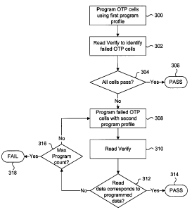
[0056] The programming cycle begins at step 300 where the cells are programmed
with default programming parameters. These parameters can include parameters
such as a
particular VPP voltage level and/or duration of the applied VPP voltage on the
selected
wordline, the duration being referred to as tPP1 (time of applied VPP). In the
present
embodiment, the selected wordline is driven to a default VPP level for a
relatively short
duration of time, such as about 50 microseconds for example. A short
programming time
minimizes power consumption, and power consumption can be further reduced if a
voltage
less than VPP is used at step 300. This reduced VPP voltage can be selected as
the lowest
VPP level for a known process technology that enables formation of a
conductive link in the
anti-fuse memory cell. Those skilled in the art understand that modeling
techniques can be
used to determine his level since the fabrication process and geometry of
memory cells is
known. Since there is no guarantee that all the cells were successfully
programmed at step
300, a program verification algorithm is executed, starting with a first read
verify operation at
step 302. This read verification step uses an aggressive first read voltage to
identify weakly
programmed cells or cells that failed to program. The first read voltage can
be a voltage
appearing on the selected wordline that is weaker than the nominal read
voltage used during
normal read operations. Use of a lower read voltage will reduce power
consumption as well.
-20-
I
CA 02690237 2010-02-05
[0057] For example, this first read voltage can be less than the nominal
positive read
voltage. Any cells that read out the expected data under this condition will
certainly read out
properly with the higher nominal read voltage. Thus, any weakly programmed
cells and failed
cells are identified at step 302 are considered cells that failed to program.
At step 302, the
cells that have properly read out are inhibited from further programming. For
example, the
anti-fuse memory cell shown in Figure 5A requires its bitline to be biased to
VSS to enable
formation of its conductive link for programming. Therefore, the bitlines for
the cells that have
properly read out are biased to VDD or some other positive voltage level to
inhibit
reprogramming. If a data register is used for storing the bits of the input
data to be
programmed, one technique to inhibit successfully programmed cells from
further
programming is to invert the input data bit stored in the data register stage
associated with
the bit, using integrated comparison logic. Another technique is to read out
the data during
step 302 and re-enter the input data with adjustments to ensure that only the
failed bits are
reprogrammed.
[0058] Returning to step 304, program verify logic in the column circuits 206
or
circuits external to the memory device determine if all the cells subjected to
programming
were successfully programmed. If all have been programmed successfully, then
the program
operation ends at step 306. Otherwise, there is at least one cell that did not
successfully
program. Proceeding to step 308, only the cells identified in step 302 as
failing to program
are programmed again with second programming parameters. For anti-fuse memory
cells,
this is also referred to as program soaking to form the conductive link or
improve the
conductive characteristics of an existing link. Ideally, all cells should be
successfully
programmed after step 308, therefore the second programming parameters can
increase the
VPP voltage level used at step 300 and/or increase the duration of application
of VPP at step
300. If a reduced VPP voltage level was used at step 300, then a default or
maximum VPP
voltage can be used at step 308. Cumulative programming should eventually
result in a
sufficiently programmed cell. In the present example, if a duration of applied
VPP time
different than tPP1 is used, then a second and different VPP application time
referred to as
tPP2 (time of applied VPP) is used. For example, tPP2 can be set to be about
500
microseconds. At step 310, a second read verify is executed to read out the
data in the
single-ended mode, but using a second read voltage greater than the first read
voltage used
at step 302.
-21-
CA 02690237 2010-02-05
[0059] It is noted that this second read voltage can be less than the nominal
read
voltage, or it can be at the nominal read voltage used during normal read
operations if an
acceptable margin is provided through timing or setting of a particular
reference voltage level
for sensing during the single-ended read mode. Furthermore, if the target read
mode is either
the differential or differential-redundant read mode, then the nominal read
voltage used
during normal read operations can be less than the second read voltage used in
the single
ended read mode verify step.
[0060] A determination is made at step 312 to see if all the bits read from
step 310
correspond to the input data. This determination can use the same techniques
previously
described for step 302. If they all the read out bits correspond to their
respective input data
bits, then the method ends at step 314 as all cells have been programmed.
Because a
nominal read voltage resulted in successful reading of all the programmed
bits, the cells
should read properly during normal single-ended read operations. Therefore the
programmed bits will read properly during any of the high reliability read
modes, as they
provide redundancy and improved read margins over the single-ended mode.
Returning to
step 312, if there is at least one cell that is read out with a logic state
that does not
correspond to its respective input bit, then the cell failed to program. In
the present
embodiment, there is no need to identify the specific cells which have failed
programming at
step 310 or step 312. The method has finished one iteration of the program
cycle, where the
number of iterations can be tracked by a counter. The method proceeds to step
316 where
the total number of iterations is compared to a predetermined maximum count.
If the total
number of iterations matches the maximum count, then it is likely that the
cell or cells that are
being repeatedly programmed are defective and unprogrammable. It is then
determined that
the program operation has failed at step 318. Otherwise, the method loops back
to step 302
for another iteration.
[0061] It is noted that cells reprogrammed at step 308 which are read properly
under
the second read voltage at step 310 may not read properly under the lower
first read voltage
of 302. Conversely, there may be cells that are sufficiently or strongly
programmed after step
308. Hence an advantage of repeating the cycle at step 302 is that these
strongly
programmed cells are inhibited from further programming, thereby reducing
power
consumption at subsequent program step 308 as there would be less cells to
reprogram.
[0062] The method then iterates until either all cells pass at step 306 or
step 314, or
until the maximum number of iterations is reached. Optionally, after the pass
status is
-22-
CA 02690237 2010-02-05
obtained at step 306 or step 314, a final read verify using the target high
reliability mode can
be executed to finally confirm that the input data has been properly
programmed. This final
read verify operation can be executed with the worst case voltage and time
parameters, for
example where a low read voltage is asserted on the selected wordlines and the
sense
amplifiers are activated in a short period of time after the selected
wordlines are driven to the
low read voltage. If the data is read out successfully under the worst case
parameters, then
the memory device has been finally validated to store the data with high
reliably.
[0063] Figure 9 is a flow chart illustrating an alternate programming
operation using
the same steps as shown in the flow chart of Figure 8, according to a present
embodiment.
Accordingly, the same reference numbers of Figure 8 are used in Figure 9 as
the same steps
are followed. In the alternate embodiment of Figure 9 the method loops back
from step 312
to step 308, as opposed to looping back to step 302 in the embodiment of
Figure 8.
Therefore the current method omits the read verify step 302 to shorten the
overall time
required for the programming operation.
[0064] The programming operations of Figures 8 or 9 are executed for each word
to
be programmed until the maximum number of iterations is reached, where a word
includes
bits of data to be programmed to the anti-fuse memory cells connected to one
wordline. The
method of Figure 8 has the advantage of identifying weakly programmed cells by
inhibiting
strongly programmed cells from further programming. Such weakly programmed
cells are
subjected to reprogramming under different programming parameters to ensure
that they are
properly programmed. The novel programming scheme combined with the high
reliability
modes of operation can further reduce erroneous reads, especially when the
memory is
operating under non-ideal temperature and voltage conditions. Alternatively, a
simplified
programming operation that does not identify weakly programmed cells could be
used to
shorten the programming time per word. In such a situation, the high
reliability modes of
operation will compensate for any programming deficiencies by reading out the
data with
high reliability. The method of Figure 9 compromises by executing only one
iteration of
identifying weakly programmed cells to shorten the programming time per word.
[0065] The presently described programming method can be used to improve
manufacturing yield if other post fabrication testing indicates that
potentially defective cells
are present. In such a case, the manufacturer can instruct end users that a
one of the high
reliability read modes should be used for the memory device. Alternately, the
manufacturer
can hardwire the read mode of the memory device with any suitable means.
-23-
CA 02690237 2010-02-05
[0066] In the preceding description, for purposes of explanation, numerous
details
are set forth in order to provide a thorough understanding of the embodiments
of the
invention. However, it will be apparent to one skilled in the art that these
specific details are
not required in order to practice the invention. In other instances, well-
known electrical
structures and circuits are shown in block diagram form in order not to
obscure the invention.
For example, specific details are not provided as to whether the embodiments
of the
invention described herein are implemented as a software routine, hardware
circuit,
firmware, or a combination thereof.
[0067] Embodiments of the invention can be represented as a software product
stored in a machine-readable medium (also referred to as a computer-readable
medium, a
processor-readable medium, or a computer usable medium having a computer-
readable
program code embodied therein). The machine-readable medium can be any
suitable
tangible medium, including magnetic, optical, or electrical storage medium
including a
diskette, compact disk read only memory (CD-ROM), memory device (volatile or
non-
volatile), or similar storage mechanism. The machine-readable medium can
contain various
sets of instructions, code sequences, configuration information, or other
data, which, when
executed, cause a processor to perform steps in a method according to an
embodiment of
the invention. Those of ordinary skill in the art will appreciate that other
instructions and
operations necessary to implement the described invention can also be stored
on the
machine-readable medium. Software running from the machine-readable medium can
interface with circuitry to perform the described tasks.
[0068] The above-described embodiments of the invention are intended to be
examples only. Alterations, modifications and variations can be effected to
the particular
embodiments by those of skill in the art without departing from the scope of
the invention,
which is defined solely by the claims appended hereto.
-24-