Note: Descriptions are shown in the official language in which they were submitted.
CA 02690795 2010-01-22
08-0913 (24691-248)
METAL BONDED NANOTUBE ARRAY
BACKGROUND OF THE INVENTION
[0001] The field of the invention relates generally to the transfer of
thermal energy away from the source of that energy, and more specifically, to
a metal
bonded nanotube array.
[0002] When the surfaces of a heat sink, such as a copper heat sink
or a graphite based chip strap, and a heat source, such as a microprocessor,
RADAR
array, or MMIC chip, are placed together to create a thermal path, there are
microscopic gaps formed by surface roughness between the heat source and the
heat
sink. Therefore, it is possible that the actual contact area between the two
surfaces is
very small and little heat may be transferred between the heat source and the
heat
sink. Current methods to address this problem include a polymer or thermal
grease
with low thermal conductivity that is placed between the two surfaces to act
as a
thermal interface material (TIM) that aids thermal transport. The flexible
filler
creates a much larger contact area between the heat source and heat sink.
However
this method generally places a low thermal conductivity material (the polymer
or
thermal grease) between the two high thermal conductivity devices (the heat
source
and the heat sink)
[0003] The above described arrangement results in a thermal
bottleneck which can be improved. For example, it would be highly advantageous
to
use a high thermal conductivity material as the thermal interface material.
However,
the only high thermal conductivity thermal interface material currently used
is solder.
When solder is utilized to join a heat source and heat sink the results are
not
advantageous because the heat sink and heat source must have very similar
coefficients of thermal expansion in order to avoid cracking of one or more of
the
solder interface, the heat source, or the heat sink.
[0004] Carbon nanotubes (CNTs) have extremely high thermal
conductivities and can act as a thermal interface material that transports
heat between
-1-
CA 02690795 2010-01-22
08-0913 (24691-248)
a heat sink and a heat source. More specifically, the individual nanotubes are
flexible
and can bend to accommodate the roughness on the opposing surfaces. In
addition,
the interface is dry and there is no concern about the TIM flowing out of the
gap
between the heat source and heat sink as there is with greases and other TIMs.
Lastly,
when the CNTs are aligned substantially adjacent one another, similar to the
strands
of a hairbrush, the CNTs are aligned perpendicularly to the substrate and
therefore can
accommodate differences in thermal expansion by bending perpendicular to the
direction along the tubes.
[0005] The use of CNTs as a thermal interface material is well
known. However, attachment of CNTs to a heat source or heat sink still
presents
certain issues. For example, there are some cases where CNTs may be grown
directly
on a heat source or heat sink. However, these cases are few due to the high
nanotube
growth temperatures of >600 C that will destroy integrated circuits or damage
heat
sinks. In all other cases, the CNTs must be grown on a growth substrate and
transferred to a heat source or heat sink post fabrication.
BRIEF DESCRIPTION OF THE INVENTION
[0006] In one aspect, a method for bonding nano-elements to a
surface is described. The method includes applying a layer of a first metal to
a first
end of a plurality of substantially aligned nano-elements, positioning a layer
of a
second metal adjacent to the layer of the first metal, positioning a substrate
adjacent to
the layer of the second metal, placing a compressive force across the nano-
elements,
the metal layers, and the substrate, and elevating the temperature of the nano-
elements, the metal layers, and the substrate such that the metal layers form
at least
one of a eutectic bond, a metal solid solution, and an alloy bond between the
nano-
elements and the substrate.
[0007] In another aspect, a thermal interface is provided. The
thermal interface includes a plurality of substantially aligned nano-elements
each
having a first end and a second end, a first metal layer bonded to the first
ends of the
nano-elements, and a second metal layer adjacent the first metal layer and
having at
-2-
CA 02690795 2010-01-22
08-0913 (24691-248)
least one of a eutectic bond, a metal solid solution, and an alloy bond
therebetween
that is operable for transferring heat between a heat source and the
substantially
aligned nano-elements.
[0008] In still another embodiment, a structure is provided. The
structure includes a plurality of substantially aligned nano-elements each
having a
first end and a second end, a first metal layer bonded to the first ends of
said nano-
elements, a second metal layer adjacent said first metal layer, and a
substrate. At least
one of a eutectic bond, a metal solid solution, and an alloy bond is formed
between
the nano-elements and the substrate through a compressive force and an
elevated
temperature across the nano-elements, the metal layers, and the substrate.
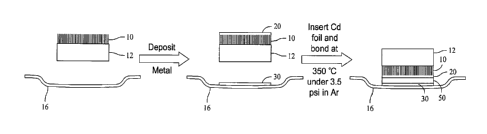
BRIEF DESCRIPTION OF THE DRAWINGS
[0009] Figure 1 is an illustration of a carbon nanotube array formed
on a silicon substrate and a thermal strap to which the nanotube array is to
be bonded.
[0010] Figure 2 illustrates deposition of copper and gold onto both
the nanotube array and the thermal strap.
[0011] Figure 3 illustrates a bonding between the nanotube array and
the thermal strap, a cadmium foil placed between the two respective
copper/gold
layers.
[0012] Figure 4 illustrates a eutectic bonding between the nanotube
array and a heat sink where the copper/gold layer is deposited on the nanotube
array
and a layer of indium is deposited on the heat sink.
[0013] Figure 5 illustrates the thermal and mechanical attachment of
a Gallium Nitrogen device to an aluminum plate.
[0014] Figure 6 is a flowchart illustrating a eutectic bonding process.
-3-
CA 02690795 2010-01-22
08-0913 (24691-248)
DETAILED DESCRIPTION OF THE INVENTION
[0015] As utilized herein, a metal eutectic bonded nanotube array is
an array of carbon nanotubes (CNTs) that are bonded to a heat source or heat
sink
using a metal eutectic bond in order to uses nanotubes as a thermal interface
material
for thermal control of a heat source. Processes that utilize metal solid
solution
bonding are also considered. As used herein, a eutectic bond describes a
melting
point of two metals that is less than the metal point of both of the metals.
In a metal
solid solution bond, the melting point of the two metals is less than the
melting point
of one of the two metals. While described herein in the context of a eutectic
bond, the
described embodiments are also operable through metal solid solution bonding.
[0016] The process associated with the eutectic bonding processs
differs from prior bonding processes in that a eutectic of two or more metals
is formed
to bond to the tips of a vertically aligned array of CNTs onto a surface that
can be the
die of a microprocessor/communication chip, a heat sink, or a graphite strap
that
attaches to a microprocessor. The eutectic bond allows the bonding of
nanotubes to
another surface to occur at a much lower pressure than the diffusion bonding
processes that are currently used.
[0017] The use of a eutectic bond between two or more metals
allows an attachment between a nanotube array and another substrate to occur
at a low
pressure. As further described herein, low pressure attachment is desirable
because
excess (or high) pressure attachment methods may result in a permanently
deformed
nanotube array. A deformed nanotube array generally will not conform to
surface
roughness between a heat source and a heat sink. It is also desirable to avoid
higher
bonding pressures because they may damage a device or heat sink.
[0018] Also disclosed herein is the use of a foil in the eutectic bond
of one of the two metals and the vacuum deposition of the other metal on one
or both
of the nanotubes and the new attachment surface (such as the side of a heat
sink). The
foil can conform to any roughness in the gap between the two surfaces to be
bonded
-4-
CA 02690795 2010-01-22
08-0913 (24691-248)
while also providing a mechanical bond to both the nanotubes and the
attachment
surface by being eutectically bonded to both opposing faces.
[0019] In order to use carbon nanotubes as a thermal interface
material, they must be placed in the interface between a heat source and a
heat sink.
One option is to form nanotubes into a thermal gasket that goes in the
interface and
the other is to attach the nanotubes to a heat source or a heat sink and have
the
nanotubes bridge the gap. In both cases, and as shown in Figure 1, the
nanotubes 10
are grown on a silicon wafer 12 and must be transferred to another surface,
such as
thermal strap 16 and subsequently bonded to this surface.
[0020] More specifically, in order to bond nanotube array 10 to
another surface, the array 10 is first grown on a silicon wafer 12 that has an
aluminum
blocking layer and a thin iron or nickel catalyst layer deposited on it (these
layers are
not shown in the figures). This substrate (silicon wafer 12) is heated under
hydrogen
to first form catalyst nanoparticles from the iron or nickel, and then the
nanotubes of
the array 10 are grown under flowing organic material (such as ethylene,
acetylene, or
toluene) and hydrogen. When the gas mixture comes into contact with iron or
nickel
nanoparticles on the surface of the wafer, carbon nanotubes form. At the end
of the
growth run a vertically aligned array 10 of nanotubes has been formed on the
wafer
12. The array 10 is then transferred onto another substrate that is a heat
sink or a heat
source.
[0021] Metals are highly useful for attaching nanotubes, and
therefore nanotube arrays, to another surface. These metals provide a high
thermal
conductivity bond and may be deposited on a nanotube array and/or the opposing
surface through sputtering, evaporation, electrodeposition, chemical vapor
deposition
(CVD), or metal organic chemical vapor deposition (MOCVD). Figure 2
illustrates a
first copper/gold layer 20 that has been deposited onto the carbon nanotube
array 10,
and a second copper/gold layer 30 that has been deposited onto the thermal
strap 16.
As further described below, a first layer of a less expensive metal (e.g.,
copper) may
be applied to the nanotube array 10, to immobilize the ends of the individual
nano-
-5-
CA 02690795 2010-01-22
08-0913 (24691-248)
elements, prior to the application of the metal used to make the eutectic bond
(e.g.,
gold). In the illustrated embodiment, a layer of copper is applied to the
nanotube
array 10 before the layer of gold is applied.
[0022] Metal layers may be attached to one another through a
diffusion bond, a solid solution bond, or a eutectic bond. Diffusion bonding
bonds
two identical metals together by heating the metals near or above the melting
point of
each of the metals and the atoms from both metals diffuse into one another.
One
problem associated with diffusion bonding is that it requires high pressure to
form the
bond. However, eutectic bonding matches two or more metals together where the
melting point of the mixture of the combination is lower than a melting
temperature of
either metal. In solid solution bonding, the melting point of the mixture of
the
combination is lower than a melting temperature of one of the two metals.
[0023] Thus when two metals are pressed together and heated below
the melting point of either metal, but above the melting point of the
eutectic, they melt
together at the interface. This process forms a bond that accommodates any
surface
roughness between the two surfaces and firmly bonds them together. Another
advantage of the eutectic bond is that the local melting where the eutectic is
formed
requires very low pressures for attachment of opposing faces. A eutectic
mixture of
two metals has a melting point that is dependant on the composition of the
mixture of
metals. If a eutectic bond that was made at the minimum melting temperature
composition is heated, diffusion of the component metals can occur which will
raise
the melting point of the bond and render it more temperature stable.
[0024] The method by which the metals, for example the above
described copper/gold combination, are placed on the nanotube array 10
controls if
attachment is successful. For example, if a thin metal foil is placed between
the
nanotube array 10 and the opposing surface of thermal strap 16, or if a thin
metal
layer is deposited on the opposing surface but not onto the nanotube array 10,
when
the sandwich of nanotubes, metal foil, and the other surface is heated, the
metal may
melt but may not infiltrate into the nanotube array 10. Thus no bond will be
created.
-6-
CA 02690795 2010-01-22
08-0913 (24691-248)
A bond will only be formed if a metal layer, such as copper/gold layer 20, is
first
deposited onto the nanotube array 10 which operates to immobilize the tips of
the
individual nanotubes. Next this metal layer is bonded onto an opposing surface
that
contains a metal that will form a eutectic with the metal coated array of
nanotubes.
As described herein, the opposing surface is generally a heat source, a heat
sink, or
another metalized nanotube array. In all the described embodiments, the metal
bonding is performed through creation of a metal-metal eutectic.
[0025] A foil is not always used. One embodiment is formed by
depositing one metal on top of the nanotubes array 10 and depositing a
different metal
that will form the eutectic is deposited on top of the opposing surface
(thermal strap
16) that will be bonded to the nanotubes array. Then the bond is created by
heating
the nanotube array 10 held against the opposing surface (thermal strap 16)
above the
eutectic melting temperature. In one specific embodiment, the opposing surface
is a
pyrolytic graphite thermal strap.
[0026] In another embodiment, the bond is formed by depositing one
metal on top of the nanotube array 10 and placing a foil of another metal that
will
form the eutectic (and wets the opposing surface) between the nanotubes and
the
opposing surface. Then the bond is created by heating the nanotube array 10
and
holding it against the opposing surface with the foil between the two, with
the heating
bringing the combination above the eutectic melting temperature.
[0027] Yet another embodiment is created by depositing one metal
onto the nanotube array 10 and also onto the opposing surface (thermal strap
16) that
will be bonded to the nanotube array 10. This embodiment is shown in Figure 3.
A
foil 50 of a second metal, in the illustrated embodiment cadmium, that will
form the
eutectic is placed between the coated nanotube array 10 and the coated thermal
strap
16 (the opposing surface). Then the eutectic bond is created by heating the
assembly
while holding the nanotube array against the opposing surface, the foil 50 in
between,
to a temperature that is above the eutectic melting temperature. though not
shown,
after the bond is made, the silicon wafer 12 may be removed.
-7-
CA 02690795 2010-01-22
08-0913 (24691-248)
[0028] A foil is not always used as illustrated in Figure 4. Figure 4
illustrates a eutectic bonding between the nanotube array 10 and a heat sink
60 where
the copper/gold layer 20 is deposited on the nanotube array 10 and a layer of
indium
62 is deposited on the heat sink 60. More generally, one metal is deposited on
top of
the nanotube array 10 and a different metal that will form the eutectic is
deposited on
top of the opposing surface, such as the heat sink 60, that is to be bonded to
the
nanotube array 10. As shown, the bond is subsequently created by holding 70
the
nanotube array 10 against the opposing surface (heat sink 60) and applying 72
heat at
a temperature that is at or slightly above the eutectic melting temperature.
In one
embodiment the bond is created in an argon environment, with a pressure of
about 6.1
psi used. For the particular metals described with respect to Figure 4, the
temperature
is about 160 degrees Celsius. After the bonding is complete, and the eutectic
74 is
formed, the silicon substrate 12 may be removed.
[0029] In a further example, illustrated in Figure 5, a Gallium
Nitrogen device is attached thermally and mechanically to an aluminum plate
that is a
substitute for an aluminum electronics housing. As in the prior Figures, four
microns
of copper and then one micron of gold (e.g., layer 20) was deposited onto the
top of
the carbon nanotube array 10 which was fabricated on the silicon wafer 12. The
carbon nanotube array 10 was separated from the silicon wafer 12, for example
with a
razor blade, and the array 10 was flipped over so that the uncoated ends of
the
nanotube array 10 were exposed. Four microns of copper and then one micron of
gold was deposited onto the carbon nanotube array 10 to form layer 80.
[0030] The aluminum plate (heat sink 82) was coated with 20
nanometers of titanium as an adhesion layer, then four microns of copper and
then
one micron of gold. A fifty micron think indium foil 84 was placed between the
nanotube metalized gasket and the aluminum plate and 6.1 psi was applied. The
stack
was heated to 180 C, while under the pressure to melt the indium. The indium
formed a solid solution (eutectic 86) with the gold deposited on the nanotubes
10 and
on the heat sink 82. Then a second fifty micron thick Indium foil 90 was
placed
between the Gallium Nitrogen device 92 and the carbon nanotube array
10/heatsink
-8-
CA 02690795 2010-01-22
08-0913 (24691-248)
82 assembly and 3.5 psi was applied and the entire assembly was heated to 180
C to
form eutectic bond 96.
[0031] Figure 6 is a flowchart 100 that further illustrates at a high
level the methods by which the above described thermal interfaces and below
described examples are fabricated. Specifically, flowchart 100 illustrates a
method
for bonding nano-elements to a surface. The method includes applying 102 a
layer of
a first metal for the eutectic bond to a first end of substantially aligned
nano-elements.
A layer of a second metal for the eutectic bond is positioned 104 adjacent to
the layer
of the first metal. The substance, sometimes referred to as a substrate, to
which the
nano-elements are to be bonded is positioned 106 adjacent to the other side of
the
layer of the second metal. A compressive force is then placed 108 across the
nano-
elements, the metal layers, and the substrate which are collectively referred
to as the
components. The temperature of the components is then elevated 110 such that
the
first metal and the second metal layers form a eutectic bond between the nano-
elements and the substance.
[0032] A couple of examples further illustrate the above described
eutectic bonding embodiments. In the first example, a 100 micron tall, one
square
centimeter carbon nanotube array and a pyrolytic graphite thermal strap for
holding a
microprocessor and transporting heat out of it are both first coated with four
microns
copper and then one micron of gold. A 0.001" cadmium foil 50 is placed between
the
metalized nanotube tips and the metalized graphite thermal strap. Three and
one-half
pounds per square inch of pressure is applied and the assembly was heated to
350 C
in an Argon atmosphere for about 45 minutes. The sample was cooled and the
nanotubes were found to be well bonded to the graphite stack. Subsequently,
the
silicon wafer was easily removed from the other side of the nanotube array. In
the
embodiment first embodiment, the melting point of Au is in excess of 1000 C,
the
melting point of Cadmium is 321 C, and the minimum melting point of a Cd-Au
eutectic is about 308 C. The bottom copper layer is deposited because it is
inert and
is more cost effective than depositing five microns of gold.
-9-
CA 02690795 2010-01-22
08-0913 (24691-248)
[0033] Another attempt at eutectic bonding was made were the
carbon nanotube array was pressed into the graphite thermal strap with only
with a
gold foil, and a cadmium foil in between. The foils created a eutectic but the
carbon
nanotube array was not infiltrated by the metals and no bonding occurred.
[0034] In the another example, a 100 micron tall, one square
centimeter carbon nanotube array and a copper plate that is a substitute for a
copper
heat sink are both coated, first with first five microns of copper and then
with five
microns of indium. A 0.001" Cadmium foil is placed between the metalized
nanotube
tips and the metal (indium) coated copper. 3.5 psi was applied and the
assembly was
heated to 120 C in an Argon atmosphere for about 45 minutes. The melting
point of
Indium is about 157 C, the melting point of Cadmium is about 321 C, and the
minimum melting point of a Cadmium-Indium eutectic is about 78 C. Once this
sample was cooled, the nanotubes were found to be well bonded to the copper
while
the silicon wafer was easily removed from the other side of the nanotube
array.
[0035] The result of this example illustrates the advantage of using
eutectic bonds due to the low required pressures and temperatures as compared
to
diffusion bonds. In comparison, a 100 micron tall, one square centimeter
carbon
nanotube array and a copper plate that is a substitute for a copper heat sink
are both
coated first with five microns of copper and then five microns of indium. To
bond the
indium faces together the array required heating to 160 C in an Argon
atmosphere for
45 minutes but with a pressure of 26 psi. The higher pressure resulted in
delaminating
of the two metalized faces. In addition, the high pressure applied for bonding
made it
difficult to remove the silicon nanotube growth substrate from the other end
of the
array as the nanotubes were compressed into a shiny black surface. Such
compression
makes it difficult for the nanotubes to conform to surface roughness as a
thermal
interface material.
[0036] In a third example, a 100 micron tall, one square centimeter
carbon nanotube array was first coated with five microns of copper and then
with five
microns of indium. A 0.001 inch Cadmium foil was placed between the metalized
-10-
CA 02690795 2010-01-22
08-0913 (24691-248)
nanotube tips and a piece of uncoated copper plate. 3.5 psi was applied and
the stack
was heated to 120 C in an Argon atmosphere for 45 minutes. The melting point
of
indium is 157 C, the melting point of cadmium is 321 C, and the minimum
melting
point of a cadmium-indium eutectic is 78 C. After the sample was cooled, the
nanotubes were found to be well bonded to the copper, and the silicon wafer
was
easily removed from the other side of the nanotube array.
[0037] In yet another example, an indium/gold solid solution (which
is similar to a eutectic, but having a variable composition, was used to
attach carbon
nanotubes to a pyrolytic graphite thermal chip cooling strap, within an argon
environment. Four microns of copper and then one micron of gold was deposited
onto the top of the carbon nanotube array. A fifty micron thick indium foil
was
placed between the array and the thermal strap. To make the bond 6.1 psi was
applied, the stack was heated to 180 C, while under the pressure to melt the
indium.
The indium formed a solid solution with the gold deposited on the nanotubes
and also
wetted the thermal strap. The liquid metal bond was cooled and the silicon
wafer base
was eventually removed from the nanotubes.
[0038] In a final example, a self soldering foil was used to attach
carbon nanotubes to the thermal strap. This example was processed in an argon
environment, but argon is not required and the process can be performed in an
air
environment. In this example, five microns of copper and then five microns of
indium are deposited onto the top of a carbon nanotube array and also onto on
the
thermal strap. A self-soldering foil is placed between the metal coated carbon
nanotube array and the metal coated thermal strap. In one preferred
embodiment, the
foil is a forty micron thick foil, such as is provided by Reactive
NanoTechnologies.
To make the bond, the silicon-carbon nanotube-foil stack is held together with
two
binder clips, and the foil is liquified with an electric pulse from a nine
volt battery.
The silicon wafer base is then removed from the carbon nanotubes. No eutectic
is
formed, however, the example illustrates another bonding method that can be
utilized
to form a low temperature, low pressure bond.
-11-
CA 02690795 2010-01-22
08-0913 (24691-248)
[0039] It is important to understand that while the described
embodiments refer to the bonding of carbon nanotubes to surfaces through
eutectic
bonds, the disclosure should not be considered to be limited to only carbon
nanotubes.
Instead the embodiments are also applicable to boron nitride nanotubes, boron
nanotubes or nanofibers, silicon nanorods, and aluminum nitride nanotubes or
nanofibers. Additional possible eutectic mixtures or metals for bonding
include
silver/bismuth, silver/cadmium, silver/indium, gold/bismuth, gold/cadmium,
gold/germanium, gold/indium, gold/tin, indium/tin, copper/tin,
bismuth/cadmium,
bismuth/indium, cadmium/copper, and indium/zinc.
[0040] The above described embodiments refer to the use of metal
foils to produce a low temperature bond between a carrier substrate and an
array of
nanotubes, for example, carbon nanotubes. In one specific embodiment, the
nanotubes have a vapor deposition of a first metal thereon at one end to
enable a
eutectic bond to a second metal placed between the nanotubes and a carrier
substrate.
Depending on the material selection, the bonding of the nanotubes with the
carrier
substrate may be improved if a layer of the first metal is first deposited
onto the
carrier substrate.
[0041] The use of the metal foils enables a bond between the
nanotubes (CNT) and the substrate to create a highly efficient thermal
interface that is
produced utilizing relatively low processing temperatures. Current methods,
such as
diffusion bonding require direct carbon nanotube growth to the substrate at
high
temperatures (>600 C). The exposure to such temperatures causes damage to
sensitive parts and/or provides an inferior solution. The described processes
allows
for processing at lower temperatures (<100 C) and results in an improved heat
transfer, for example, from a die processing chip. Such embodiments likely
have
application, for example, in electronics applications where heat removal is
required.
[0042] Heat removal limits processing power in various applications,
such as missiles and satellites, however there are many other applications
where heat
removal remains a problem that impacts over all performance. The use of
improved
-12-
CA 02690795 2010-01-22
08-0913 (24691-248)
thermal interface materials enables greater processing capabilities and longer
product
lifetimes by reducing system temperature in these products. Finally, the
described
embodiments enable increased heat removal from power electronics and
electronics
boxes in both vehicles and non-mobile devices.
[0043] This written description uses examples to disclose the
invention, including the best mode, and also to enable any person skilled in
the art to
practice the invention, including making and using any devices or systems and
performing any incorporated methods. The patentable scope of the invention is
defined by the claims, and may include other examples that occur to those
skilled in
the art. Such other examples are intended to be within the scope of the claims
if they
have structural elements that do not differ from the literal language of the
claims, or if
they include equivalent structural elements with insubstantial differences
from the
literal languages of the claims.
-13-