Note: Descriptions are shown in the official language in which they were submitted.
CA 02690823 2009-12-14
WO 2008/157550 PCT/US2008/067231
MATRIX ASSISTED INK TRANSPORT
RELATED APPLICATIONS
This application claims priority to US provisional serial no. 60/945,164 filed
June 20, 2007, and also to US provisional serial no. 60/929,314 filed June 21,
2007,
and also to US provisional serial no. 61/047,642 filed Apri124, 2008, all of
which are
hereby incorporated by reference in their entireties.
STATEMENT ON FEDERAL FUNDING
The present invention was developed with use of federal funding from NSF-
NSEC, Grant No. EEC 0118025; and DARPA-ARD, Grant No. DAAD 19-03-1-
0065; and NSF Grant No. EEC0647560; and ASAF/AFOSR FA9550-08-1-0124. The
federal government reserves rights in the invention.
BACKGROUND
Nanoscience focuses on elucidating the unique chemical and physical
properties of nanoscale materials that analogous bulk structures do not
possess (37,
38). Bottom-up and top-down approaches have been used to synthesize and
fabricate
such nanoscale materials that are metallic (1, 4, 5, 11), magnetic (6,7), semi-
conducting (8,9), silica-based (18), and carbon-based, such as fullerenes, and
carbon
nanotubes, (3, 73) with fine control over particle size and shape (74, 36). In
the last
decade, nanoscale materials have been studied and characterized using a
variety of
methods and are becoming better understood.
Nanoscale materials are beginning to be utilized in a growing number of novel
applications including applications, that rely mainly on the ability to
arrange nano
building blocks (NBBs) into deliberate patterns with controlled feature sizes
on
surfaces, such as nanocircuit integration (75), biological micro- and nano-
array
fabrication (76) , and nanoscale sensing (77, 78). Current methods for
patterning
nano building blocks into desired locations usually include the following two
steps: 1)
a surface pattern-generation step and 2) a nanoparticle self-assembly step.
The first
step creates pre-patterns on a surface using photolithography, electron beam
-1-
CA 02690823 2009-12-14
WO 2008/157550 PCT/US2008/067231
lithography (EBL), or focused ion beam (FIB) lithography (79), while in the
second
step, nanoparticles are exposed to and further assembled along the pre-
pattemed areas
on the surface (39). Unfortunately, such surface patterning methods can
require
expensive instrumentation and may be complicated and time-consuming. For
example, avoiding non-specific binding of nanoparticles to unwanted areas
during the
second step may be often a very difficult, if not impossible task. Such
problem can be
especially prominent at the sub-100 nm size regime.
Dip-pen nanolithography (DPN) is a single-step direct writing and reading
lithography tool utilized for patterning soft inks, such as small organic
molecules,
DNA, and proteins (60), in some cases, at the millimeter and centimeter scale
(61,62).
In some cases, it may be more difficult to directly write hard inks, such as
nanoparticles, fullerenes, or crystallized conducting polymers, using DPN due
to
problems with obtaining an even coating of such hard inks on an AFM tip and
controlling the ink's transport rate. As the result, the nanoparticle patterns
may
become inconsistent and have uncontrollable feature sizes. In addition, hard
inks may
in some cases have a tendency to dry quickly and agglomerate during the DPN
process, which makes extended writing times unachievable (63-68).
Thus, a need exists to develop a single step method for direct patterning of
hard inks on a surface that will provide a control over the patterned feature
size and
will allow for longer writing times. In particular, development of direct
patterning
methods for protein-based nanostructures is important for researchers working
in the
areas of proteomics and theranostics. Such methods would allow generating
multi-
component biological nanostructures of proteins, oligonucleotides and viruses.
US Patent No. 7,005,378 describes patterning of metallic precursors including
use of polyethylene oxide to facilitate patterning.
The paper "On-Wire Lithography" (Qin et al., Science, vol. 309, July 1, 2005,
113-115) describes preparation of gap structures and filling the gap with a
mixture of
a conductive polymer and polyethylene oxide.
US Patent Publication 2003/0162004 (Mirkin et al., Northwestern University)
describes patterning of sol-gel mixtures comprising block copolymers.
-2-
CA 02690823 2009-12-14
WO 2008/157550 PCT/US2008/067231
US Patent Publication 2004/0142106 (Mirkin et al., Northwestern University)
describes patterning of precursor magnetic materials.
US Patent Publication 2002/0122873 (Mirkin et al., Northwestern University)
describes patterning of magnetic nanoparticles using magnetic driving forces.
US Patent Publication 2004/0026007 (Hubert et al., MIT) describes deposition
of nanoparticles.
SUMMARY
The present application describes among other things methods of making,
articles, devices, compositions, and methods of using.
One embodiment provides a method comprising: providing a tip, providing an
ink disposed at the end of the tip, wherein the ink comprises at least one
matrix and at
least one nanomaterial different from the matrix, providing a substrate
surface, and
transporting the ink from the tip to the substrate surface to form a structure
on the
surface comprising both the matrix and the nanomaterial.
In another example, provided is a method comprising: providing a tip,
providing an ink disposed at the end of the tip, wherein the ink comprises at
least one
polymer and at least one nanomaterial, providing a substrate surface, and
transporting
the ink from the tip to the substrate surface to form a structure on the
surface
comprising both the polymer and the nanomaterial.
One advantage for at least one embodiment is that it allows forming patterns
of inks that may be difficult to pattern. Another advantage for at least one
embodiment is that it does not require chemical or physical modification of
the tip or
stamp. In addition, this in many cases does not require chemical or physical
modification of the substrate surface and allows transporting ink molecules to
the
surface in a fashion that is independent of the substrate surface's material.
In many
embodiments, the method allows sub-micron and sub 100-nm patterns of hard inks
such as nanomaterials and biomolecules such as proteins or peptides in a
direct write
high-throughput manner.
-3-
CA 02690823 2009-12-14
WO 2008/157550 PCT/US2008/067231
BRIEF DESCRIPTION OF THE DRAWINGS
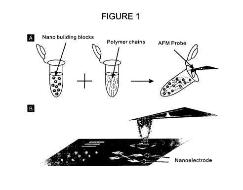
FIGURE 1 schematically illustrates patterning of nanomaterials using matrix
assisted
Dip-Pen nanolithography (DPN).
FIGURES 2 (A)-(F) present DPN generated patterns of various polymers on a
variety
of substrates as well as selected height profiles. (A) is a topographic atomic
force
microscopy (AFM) image of a pattern of polyethylene glycol (PEG) with
molecular
weight (MW) 8,000 on an Au substrate at writing speed of 0.16 m/s. (B) is an
AFM
image of a pattern of PEG (MW 8,000) on a GaAs substrate at writing speed of
0.022
m/s. (C) is an AFM image of a pattern of polyethylene oxide (PEO) with MW
100,000 on a SiOX substrate at writing speed of 0.05 m/s. (D) is an AFM image
of a
pattern of PEO (MW 100,000) on an Au substrate at writing speed of 0.05 m/s.
(E)
is an AFM image of a pattern of polyethylene imine (PEI) with MW 10,000 on
InAs
at 0.6 and 0.3 m/s. (F) is an AFM image of a pattern of a mixture of PEI (MW
10,000) and 2 nm Au nanoparticles on InAs at 0.6 and 0.3 m/s.
FIGURES 3 (A) and 3 (B) present height profiles of line patterns of: (A) PEI
only;
(corresponding topographic AFM image n FIG. 2E) and (B) a mixture of 2 nm Au
nanoparticles and PEI on InAs substrate (corresponding topographic AFM image
in
FIG. 2F). FIGURE 3(C) is a height profile of PEO only line patterns on Au
(corresponding AFM topographic image was shown in FIG. 2D).
FIGURES 4 (A)-(D) present images DPN generated arrays. (A) is a topographic
AFM image of PEO arrays at contact time of 64, 32, and 16 seconds from top to
bottom, respectively. (B) shows a topographic AFM image of dot arrays
deposited
using a mixture 2 nm Au nanoparticles and PEO, tip substrate contact time is
64, 32
and 16 seconds from top to bottom respectively. (C) is a topographic AFM image
of
dot arrays using deposited using a mixture of 5 nm Au nanoparticles and PEO,
tip-
substrate contact times 64, 32, 16, and 8 from top to bottom respectively, the
inset
-4-
CA 02690823 2009-12-14
WO 2008/157550 PCT/US2008/067231
shows a Transmission Electron Microscopy (TEM) image of the dot created by DPN
on a TEM grid. (D) shows a topographic AFM image of dot arrays deposited using
a
mixture 13 nm Au nanoparticles and PEO, tip substrate contact time is 64, 32
and 16
seconds from top to bottom respectively.
FIGURES 5 (A)-(D) present images of patterns generated by DPN using a mixture
of
4.7 nm magnetic nanoparticle and PEO. (A) is an AFM image of dot arrays, tip
substrate contact time is 64, 32 and 16 seconds from top to bottom
respectively. (B)
is an AFM image of diamond shape line arrays, writing speed 0.05 m/s. (C) is
a
magnetic force microscopy (MFM) image of larger scale dot arrays. The inset
shows
a single dot scan (G) is a MFM image of an array of diamond shaped lines
created by
DPN. The inset shows a single diamond shape line scan.
FIGURES 6 (A)-(D) relate to arrays generated by DPN using a mixture of
fullerene
and PEO. (A) is an AFM image of dot arrays at contact times of 16, 8 and 4
seconds
from top to bottom respectively. (B) is a height profile of the dot arrays of
(A). (B)
presents line arrays at writing speed of 0.05, 0.1 and 0.2 m/s respectively.
(C) is a 3-
dimensional AFM image of DPN generated lines crossing through the 500 nm gap
nanoelectrode. (F) shows I-V curves of the lines of (E).
FIGURES 7 (A) and (B) are respectively a topographic AFM image (A) and a
height
profile (B) of fullerene/PEO dot patterns on Au substrate generated by DPN.
Contact
times are 64, 32, and 16 sec from top to bottom of FIG. 7A, respectively.
FIGURE 7
(C) is a height profile of fullerene/PEO line patterns on Au substrate
generated by
DPN at writing speeds of 0.05, 0.1, and 0.2 m/s from left to right,
respectively. The
corresponding AFM topography image was shown in FIG. 6B.
FIGURE 8 schematically illustrates generating of protein arrays.
FIGURES 9 (A) and (B) present AFM images of anti-chicken IgG AF 488 nanoarrays
on Au (A) and silicon (B) surfaces generated by matrix assisted (MA) -DPN.
-5-
CA 02690823 2009-12-14
WO 2008/157550 PCT/US2008/067231
FIGURE 10 shows fluorescence microscopy images of anti-chicken IgG AF 488
nanoarrays generated by MA-DPN on silicon substrates.
Figure 11. (A) Plots showing the relationship of the DPN-generated dot sizes
with tip-
substrate contact time of selected ink materials, the slopes of the plot
reflect the
according ink's diffusion constant. (B) Charts showing the change of the ink
(anti-
ubiquitin) diffusion rate with the adding of PEO at different ratios. (C)
Comparison of
the diffusion rate of BSA/PEO and anti-ubiquitin/PEO at ratio of 1:5, the
chart shows
very close diffusion rate. (D) Charts showing that the ink diffusion rate of
IgG and (3-
galactosidase can be tuned to be very close at the ink/PEG ratio of 1:5 and
1:7.5,
respectively.
Figure 12. (A) Fluorescent image of DPN generated dot arrays. The AFM tips
were
coated one after another with BSA/PEG (green) and anti-ubiquitin/PEG (red),
respectively, both at ratio of 1:5, and both inks were simultaneously
patterned using
passive one dimensional A-26 AFM tip array. (B) Zoomed-in image of the area
within
the rectangular in (A), which shows sharp fluorescent signal contrast. (C) and
(E),
AFM images of DPN generated nanoarrays containing IgG/PEG (1:5) and (3-
galactosidase/PEG (1:7.5), respectively. (D) and (F), fluorescent images of
the
nanoarrays in (C) and (E) after incubating with according fluorescent labeled
antibodies.
Figure 13. (A) Overview and (B) zoomed-in area of the inkwell that used for
alternative two ink (BSA/PEG and anti-ubiquitin/PEG) coating. (C) Optical and
(D)
fluorescent microscopy images of the AFM tip array (A-26) used for multiple-
ink
patterning by DPN. (E) Overview and (F) zoomed-in area of the inkwell that
used for
IgG/PEG and R-galactosidase/PEG coating. Inkwell and tip arrays available from
Nanolnk, Inc. (Skokie, IL).
-6-
CA 02690823 2009-12-14
WO 2008/157550 PCT/US2008/067231
DETAILED DESCRIPTION
INTRODUCTION
Priority US provisional serial no. 60/945,164 filed June 20, 2007, and
priority
US provisional serial no. 60/929,314 filed June 21, 2007, and also priority US
provisional serial no. 61/047,642 filed Apri124, 2008, are all hereby
incorporated by
reference in their entireties, including working examples, figures, claims,
and
description of various embodiments.
Copending application serial no. filed on same day as this
application, "Patterning with Compositions Comprising Lipids," to Mirkin et
al., is
hereby incorporated by reference in its entirety including figures, claims,
working
examples, and description of other embodiments.
Copending application serial no. filed on same day as this
application, "Universal Matrix," to Mirkin et al., is hereby incorporated by
reference
in its entirety including figures, claims, working examples, and description
of other
embodiments.
Nanolithography instruments and accessories, including ink wells and pen
arrays, for direct-write printing can be obtained from Nanolnk, Inc., Chicago,
IL. DIP
PEN NANOLITHOGRAPHY and DPN are registered Nanolnk, Inc. trademarks.
The following patents and co-pending applications relate to direct-write
printing with use of for example cantilevers, tips, and patterning compounds
are
hereby incorporated by reference in their entirety:
U.S. patent No.6,635,311 issued October 21, 2003 ("Methods Utilizing
Scanning Probe Microscope Tips and Products Therefor or Produced Thereby") to
Mirkin et al., which describes fundamental aspects of DPN printing including
inks,
tips, substrates, and other instrumentation parameters and patterning methods;
U.S. patent No. 6,827,979 issued December 7, 2004 ("Methods Utilizing
Scanning Probe Microscope Tips and Products Therefor or Produced Thereby") to
Mirkin et al., which further describes fundamental aspects of DPN printing
including
software control, etching procedures, nanoplotters, and arrays formation.
-7-
CA 02690823 2009-12-14
WO 2008/157550 PCT/US2008/067231
U.S. patent publication number 2002/0122873 Al published September 5,
2002 ("Nanolithography Methods and Products Produced Therefor and Produced
Thereby"), which describes aperture embodiments and driving force embodiments
of
DPN printing.
U.S. patent publication 2003/0185967 to Eby et al., published October 2, 2003
("Methods and Apparatus for Aligning Patterns on a Substrate"), which
describes
alignment methods for DPN printing.
U.S. patent No. 7,060,977 to Dupeyrat et al., issued June 13, 2006
("Nanolithographic Calibration Methods"), which describes calibration methods
for
DPN printing.
U.S. Patent Publication 2003/0068446, published April 10, 2003 to Mirkin et
al. ("Protein and Peptide Nanoarrays"), which describes nanoarrays of proteins
and
peptides;
U.S. Regular Patent Application, Ser. No. 10/307,515 filed Dec. 2, 2002 to
Mirkin et al. ("Direct-Write Nanolithographic Deposition of Nucleic Acids from
Nanoscopic Tips"), which describes nucleic acid patterning.
U.S. Patent Publication 2003/0162004 to Mirkin et al. published August 28,
2003 ("Patterning of Solid State Features by Direct-Write Nanolithographic
Printing"), which describes reactive patterning and sol gel inks.
U.S. Patent No. 6,642,129, issued November 4, 2003, to Liu et al. ("Parallel,
Individually Addressible Probes for Nanolithography").
U.S. Patent No. 6,737,646, issued May 18, 2004, to Schwartz ("Enhanced
Scanning Probe Microscope and Nanolithographic Methods Using Same").
U.S. Patent No. 6,674,074 issued January 6, 2004, to Schwartz ("Enhanced
Scanning
Probe Microscope").
U.S. Patent No. 7,098,058 issued August 29, 2006.
U.S. Patent publication 2004/0026681 published February 12, 2004.
U.S. Patent No. 7,005,378 issued February 28, 2006.
U.S. Patent Publication 2004/0175631 published September 9, 2004.
U.S. Patent No. 7,034,854 issued Apri125, 2006.
U.S. Patent Publication 2005/0009206 published January 13, 2005.
-8-
CA 02690823 2009-12-14
WO 2008/157550 PCT/US2008/067231
U.S. Patent Publication 2005/0272885 published December 8, 2005.
U.S. Patent Publication 2005/0255237 published November 17, 2005.
U.S. Patent Publication 2005/0235869 published October 27, 2005.
U.S. Patent publication 2006/0040057 to Sheehan et al. (Thermal Control of
Deposition in Dip Pen Nanolithography).
Two dimensional arrays are described in US Patent publication no.
2008/0105042 to Mirkin et al., filed March 23, 2007, which is hereby
incorporated by
reference in its entirety including figures, claims, working examples, and
other
descriptive embodiments.
In some embodiments, the direct-write nanolithography methods described
herein can be particularly of interest for use in preparing bioarrays,
nanoarrays, and
microarrays based on peptides, proteins, nucleic acids, DNA, RNA, viruses, and
the
like. See, for example, US Patent No. 6,787,313 for mass fabrication of chips
and
libraries; 5,443,791 for automated molecular biology laboratory with pipette
tips;
5,981,733 for apparatus for the automated synthesis of molecular arrays in
pharmaceutical applications;
Direct write methods, including DPN printing, are described in for example
Direct- Write Technologies, Sensors, Electronics, and Integrated Power
Sources,
Pique and Chrisey (Eds), 2002.
Scanning probe microscopy is reviewed in Bottomley, Anal. Chem., 1998, 70,
425R-475R. Scanning probe microscopes are known in the art including probe
exchange mechanisms as described in US Patent No. 5,705,814 (Digital
Instruments).
The inventors developed a method of patterning utilizing a mixture that
comprises a polymer and a nanomaterial. In an embodiment of the method, the
mixture is first disposed on a tip or stamp and then transported from the tip
or stamp
on a substrate surface to form a pattern on the surface that comprises the ink
of
choice. The method as applied for Dip Pen Nanolithography printing is
illustrated on
Figure 1.
-9-
CA 02690823 2009-12-14
WO 2008/157550 PCT/US2008/067231
INK
Ink can be transported to a surface whether from a tip or a stamp or some
other
transport originating surface. The ink can be a composite material and can
comprise
at least two components including at least one polymer and at least one
nanomaterial,
the nanomaterial being different than the polymer. The ink can be initially
formulated
with use of a solvent and may further comprise solvent or at least residual
solvent for
the polymer. In many cases, solvent is removed upon disposing the ink at the
end of a
tip or on a stamp surface. In other cases, the ink yet comprises solvent and
is used as
a liquid. For example, ink can be delivered by channels to the end of a tip.
A basic and novel feature can be that the ink consists essentially of the
polymer and the nanomaterial and is substantially free of components that
interfere
with transport of polymer and nanomaterial. In some cases, the ink comprises
at least
at least 70%, or at least 90% by weight polymer and nanomaterial. The ink can
comprises less than 30% by weight or less than 10% by weight material which is
not
polymer or nanomaterial.
POLYMER
The ink carrier matrix is usually chosen as any material that can be
relatively
easily patterned by DPN printing. If a specific feature size and particular
patterns are
desired, the polymer material of the ink carrier matrix can be any material
that can be
easily patterned by DPN in a well controlled manner as to provide the desired
feature
size and pattern when used by itself. Preferably, the polymer ink carrier
matrix is
selected to be such that it satisfies at least some of the following criteria:
1) the polymer ink carrier matrix does not chemically react with either the
molecules of the ink or the material of the tip or stamp;
2) a transport rate of the polymer ink carrier matrix is a higher than a
transport
rate of the ink mixed with the matrix;
3) the polymer ink carrier matrix does not interfere with inherent physical or
biological characteristics of the ink.
The ink carrier matrix can be, for example, a polymer matrix. The polymer
can be a non-biological polymer. The polymer can be a soluble polymer; it can
be a
-10-
CA 02690823 2009-12-14
WO 2008/157550 PCT/US2008/067231
linear polymer having a linear polymer backbone or only small amount of
branching.
The polymer can be a copolymer, a block copolymer, a random copolymer, a
terpolymer, or a branched polymer. A polymer can be functionalized for
crosslinking
although in many cases this is not desired, particularly if the polymer is to
removed by
solvent washing.
The polymer can be soluble in both water as well as organic solvent or non-
aqueous solvent.
A polymer forming the polymer matrix can be, for example, polyalkylene
oxide, polyalkylene glycol, or polyalkylene imine. In some embodiments,
polyalkylene oxide used as a polymer matrix can be a polyalkylene oxide having
a
molecular weight over 50,000. Yet, in some embodiments, a polyalkylene oxide
having a molecular weight of about 50,000 or less can be used.
In some embodiments, polyethylene oxide (PEO) having a molecular weight
(MW) of about 100,000 can be preferred as a material for the polymer matrix.
Such a
polymer has a low melting temperature and can be easily patterned by itself
using
DPN.
In general, PEO does not react with many hard inks or biomaterials and thus
does not effect their chemical, biological or physical characteristics. In
addition, PEO
is soluble in a variety of solvents including both hydrophilic and hydrophobic
solvents, both aqueous and organic solvents, both polar and non-polar
solvents. The
good solubility makes PEO compatible with a variety of inks. For example,
fullerenes or carbon nanotubes can be mixed with PEO using toluene as a common
solvent; magnetic nanoparticles can be mixed with PEO using dichloromethane as
a
common solvents; Au nanoparticles or water soluble conducting polymers, such
as
sulphonated polyaniline (SPAN) or doped polypyrrole, can be mixed with PEO
using
water as a common solvent; quantum dots can be mixed with PEO using hexane as
a
common solvent; biomolecules such as nucleic acids or proteins can be mixed
with
PEO utilizing an appropriate biological buffer as a common solvent. Moreover,
PEO
can be patterned on a variety of substrate surfaces including metal surfaces
such as Au
surface, semiconductor surfaces such as GaAs or InAs surface or oxide surface
such
-11-
CA 02690823 2009-12-14
WO 2008/157550 PCT/US2008/067231
as SiO,t surface. Lower molecular weight PEO, also sometimes called
polyethylene
glycol, can be used.
The polymer and substrate surface can be adapted so that the polymer does not
chemisorb to or covalently bond with the surface. Also, the polymer and the
nanomaterial can be adapted so that the polymer is not chemically reactive
with the
nanomaterial.
NANOMATERIAL
Nanomaterials can be particulate types of materials having at least one
lateral
dimension of at least about 100 nm or less, or about 50 nm or less, or about
25 nm or
less. The nanomaterial can be for example a spherical material, or a
substantially
spherical material, or an elongated material. For example, a fullerene for
purposes
here can be considered a substantially spherical material. This lateral
dimension can
be a statistical average for many distinct units or particles. It can be for
example an
average particle diameter for substantially spherical particles or an average
particle
length or width for elongated particles. The nanomaterial can be organic or
inorganic,
hard or soft, flexible or rigid. The nanomaterial can be a non-molecular
material. In
preferred embodiments, the nanomaterial can be for example a metal
nanoparticle, a
magnetic nanoparticle, or a fullerene nanoparticle.
While the methods described herein can be applied to delivery of a wide
variety of ink nanomaterials, in many cases, the ink nanomaterial can be a
material
that is difficult to pattern by itself, without a polymer as ink carrier
matrix, using DPN
printing for example. For example, the transport rate may be too slow or the
transporting too unreliable.
For instance, the ink of choice can be a hard ink including metal
nanoparticles
such as Au or Ag silver nanoparticles, semiconductor nanoparticles as quantum
dots,
oxide nanoparticles such as silica or alumina particles, magnetic particles,
carbon-
based particles such as fullerenes and carbon nanotubes, crystalline polymers
including crystalline conducting polymers.
The method is not limited to patterning hard inks and can be used also for
patterning soft inks including biomaterials, biomolecules, or biological
-12-
CA 02690823 2009-12-14
WO 2008/157550 PCT/US2008/067231
macromolecules such as nucleic acids, DNA, RNA, proteins, peptides,
polypeptides,
antibodies, and oligo- and polysaccharides. Crystallized conducting polymer
can be
used.
In an embodiment, the nanomaterial comprises a nanoparticle nanomaterial.
The nanomaterial can comprise a nanoparticle comprising an average particle
size of
about 2 nm to about 100 nm, or about 2 nm to about 25 nm.
In other embodiments, the nanomaterial can be a carbon nanotube, whether
single, double, or multi-walled. The nanomaterial can comprise a nanowire or a
nanorod. The nanomaterial can comprise a semiconductor-related material and be
for
example a quantum dot.
The nanomaterial and substrate surface can be adapted so that the
nanomaterial does not chemisorb to or covalently bond with the surface.
TIPS AND STAMPS
The tip embodiment will be further described. The stamp embodiment will
also be further described. Many of the parameters described herein such as the
selection of the patterning compound, surface, and contact conditions can be
used for
both tip and stamp embodiments. Tips and stamps are used in other technologies
besides DPN printing and microcontact printing.
Tips known in art of DPN printing can be used. Sharp tips can be used which
are characterized by a sharp, pointed end. The tip can be for example a
nanoscopic
tip. The tip can be for example a scanning probe microscope tip or an atomic
force
microscope tip.
Tips can be engineered to be useful for scanning probe or AFM measurements
if suitably adapted with for example cantilever and feedback mechanism. In
particular, the tip can be disposed at the end of a cantilever. The tip can be
a hollow
tip or a solid tip or a non-hollow tip. The tip can comprise a channel for
delivery of
the ink mixture. Tips including solid, non-hollow, and hollow tips are further
described in for example US Patent Nos. 6,635,311 and 6,827,979, as well as
2002/0122873, which are herein incorporated by reference in their entirety. WO
-13-
CA 02690823 2009-12-14
WO 2008/157550 PCT/US2008/067231
2005/115630 to Henderson et al, published December 8, 2005, also describes an
elongated beam with elongated aperture for deposition on surfaces. See also US
Patent Publication 2006/0096078 to Bergaud et al. for deposition based on slit
or
groove technology; see also, Espinosa et al., Small, 1, No. 6, 632-635, 2005
for
nanofountain probe writing; Lewis et al., Appl. Phys.Lett., 1999, 75, 2689-
2691; Taha
et al., Appl. Phys. Lett., 2003, 83, 1041-1043; Hong et al, Appl. Phys. Lett.,
2000, 77,
2604-2606; Meister et al., Microelectron. Eng., 2003, 67-68, 644-650; Deladi
et al.,
Appl. Phys. Lett., 85, 5361-5363.
Tips can comprise hard inorganic, ceramic materials, or softer organic
materials. Semiconductor materials can be used. Insulative and conductive
materials
can be used. Tips known in the art of AFM imaging, for example, can be used
including silicon or silicon nitride. For example, polymer or polymer-coated
tips can
be used. See, for example, US Patent Publication No. 2005/0255237 to Zhang et
al,
which is herein incorporated by reference in its entirety. Polymer tips and
cantilevers
are described in, for example, Mirkin and Liu, US Patent Publication No.
2004/0228962, related to scanning probe contact printing.
The tip disposed on the cantilever can be part of a larger structure
comprising
a plurality of tips disposed on a plurality of cantilevers. These can be
called multipen
structures or parallel pen structures. For example, the multipen structure can
have
over 20, or over 100, or over 1,000, or over 10,000, or over 100,000, or over
1,000,000 individual tips. The cantilevers and tips can be adapted for
individual
actuation, wherein one tip can be raised or lowered independently of another
tip.
Individual actuation is described in for example US Patent Nos. 6,867,443 and
6,642,129 to Liu et al, which are hereby incorporated by reference in their
entirety.
Electrostatic or thermal actuation can be used.
Tips can be thermally heated and activated for temperature control. In
particular, the tip can be heated to effect transport.
Tips can comprise an inorganic surface and tips can be used where they are
not modified after fabrication with an organic material or coating.
In one embodiment, a plurality of tips can be provided comprising ink
disposed at the end of the tip, and transporting ink from the tips to the
substrate
-14-
CA 02690823 2009-12-14
WO 2008/157550 PCT/US2008/067231
surface forms a plurality of structures on the surface comprising both the
polymer and
the nanomaterial.
In addition, stamps can be used including stamps for microcontact printing can
be used. See for example Xia and Whitesides, "Soft Lithography," Angew. Chem.
Int. Ed., 1998, 37, 550-575, and references cited therein, for description of
microcontact printing including stamps (pages 558-563). In general, stamps are
fabricated for massive parallel printing using Z direction motion rather than
serial
motions with fine XY motion. Stamps can comprise a single material or can be
formed by multilayering methods including surface treatments to improve
printing.
One surface layer can supported which has different properties than the
support, e.g.,
stiffer. The stamp can comprise a polymer including an elastomer or a
crosslinked
rubber, such as, for example, a hydrophobic polymer, such as a silicone
polymer or
siloxane polymer, which is adapted for accepting ink but also depositing ink.
The
stamp can be patterned to form lines, including straight and curvilinear
lines, or
circles or dots.
The stamp can be fabricated to have very small structures, which can be a tip.
In addition, surfaces can be used which provide relief structures. Here, some
areas of
the surface rise above other areas of the surface, and the ink primarily coats
the raised
up areas.
One of the advantages of the present method is that it does not require
chemical or physical modification of the tip or stamp. I.e. in some
embodiments, the
tip or stamp can be an unmodified tip or stamp, i.e. a tip or stamp not
exposed to
chemical or physical modification prior to having a mixture comprising an ink
and ink
carrying matrix being disposed on the tip or stamp.
The chemical or physical modification of the tip or stamp is usually used in
the prior art methods to promote or enhance ink coating to the tip or stamp,
to
promote or enhance ink adhesion to the tip or stamp and/or to promote or
enhance ink
transport from the tip or stamp to the substrate surface. Examples of chemical
or
physical modification of the tip or stamp include but not limited to base
treatment to
impart a charged surface of the silicon nitride tip, silinization with amino-
or
-15-
CA 02690823 2009-12-14
WO 2008/157550 PCT/US2008/067231
mercaptosilanizing agents, non-covalent modification with small molecules or
polymeric agents such as polyethyleneglycol (PEG).
SUBSTRATE SURFACE
The substrate surface can be a surface of any substrate although the surface
can be adapted to function with the ink, the polymer, the nanomaterial, and
the
application at hand. Smother substrates are generally preferred for providing
pattern's
higher resolution. For example, the substrate surface can be a surface of an
insulator
such as, for example, glass or a conductor such as, for example, metal,
including gold.
In addition, the substrate can be a metal, a semiconductor, a magnetic
material, a
polymer material, a polymer-coated substrate, or a superconductor material.
The
substrate can be previously treated with one or more adsorbates. Still
further,
examples of suitable substrates include but are not limited to, metals,
ceramics, metal
oxides, semiconductor materials, magnetic materials, polymers or polymer
coated
substrates, superconductor materials, polystyrene, and glass. Metals include,
but are
not limited to gold, silver, aluminum, copper, platinum and palladium. Other
substrates onto which compounds may be patterned include, but are not limited
to
silica, silicon oxide SiOX, GaAs, InP and InAs.
One of the advantages of the present method is that it does not require for a
substrate surface to be chemical or physical modified prior to transporting
the mixture
comprising the ink and the ink carrier matrix to the substrate surface.
Accordingly, in
some embodiments, the substrate surface can be an unmodified substrate
surface, i.e.
a substrate surface, which was not chemically or physically modified prior to
being
patterned.
The chemical or physical medication of the substrate surface is usually used
in
the prior art methods to promote ink transport from the tip or stamp to the
substrate
surface, to enhance ink adhesion to the substrate surface or to covalently
modify the
substrate surface. Examples of physical or chemical modification of the
substrate
surface include but not limited to base treatment of a charged surface of
silicon oxide,
silanization with amino or mercaptosilinizing agents or modification with
polymers
carrying chemically reactive groups.
-16-
CA 02690823 2009-12-14
WO 2008/157550 PCT/US2008/067231
Another advantage of the present method that it does not require prepatterning
of the substrate surface.
The substrate can be monolithic or comprise multiple materials including
multiple layers. In a preferred embodiment, the substrate surface is a
semiconductor
or metal substrate surface.
The substrate surface can present conductive portions, insulative portions, or
both. The conductive portions can be electrodes for example. The ink can be
transported onto or in between electrodes, establishing contact with
electrodes.
INK TRANSPORT
The mixture can be transported from a tip or stamp to a substrate surface in
several different ways and is not in particular limited. Known methods in DPN
printing and microcontact printing can be used. For instance, in scanning
probe and
AFM-related technology, different modes can be used to have tips interact with
surfaces, which include contact mode, non-contact mode and intermittent
contact
mode or tapping mode. Cantilevers can be oscillated. Known feedback methods
czn
be used for positioning and alignment the X, Y and Z directions.
The transporting of the mixture from the tip to the surface can be carried out
by moving the tip only in the Z direction up and down with respect to the XY
plane of
the substrate surface to engage with and disengage with the surface. A contact
time
can be used and if contact is what activates ink flow then ink flows during
the the
contact time. The mixture delivery can be performed without translating the
tip over
the substrate surface, without moving in the XY plane, and holding the tip
stationary.
Alternatively, the tip can be translated over the surface, moving in the XY
plane.
Either the tip can be moved and the surface held stationary, or the surface
can be
moved and the tip held stationary.
The transporting can be carried out under conditions such as humidity,
temperature, and gaseous atmosphere which provide for a water meniscus between
the
tip and surface. For example, relative humidity can be at least about 25%, or
at leact
about 40%, or at least about 50%, or at least about 70%. Conditions can be
controlled
with use of environmental chambers. The gaseous atmosphere can be air, an
inert
-17-
CA 02690823 2009-12-14
WO 2008/157550 PCT/US2008/067231
atmosphere, an atmosphere with controlled humidity, or with the presence of
other
volatile or gaseous compounds such as vapors of organic compounds or volatile
solvents such as alcohols like methanol or ethanol. Conditions can be selected
to not
favor a water meniscus including, for example, anhydrous conditions or
conditions
wherein all reagents and surfaces are selected to be free of water.
The transporting can be done manually or by instrument with computer
control. Software can be used which can facilitate pattern design,
calibration,
leveling, and alignment. Calibration methods are described in for example US
Patent
No. 7,060,977 to Cruchon-Dupeyrat et al., which is hereby incorporated by
reference.
Alignments methods are describe in for example 2003/0185967 to Eby et al.,
which is
hereby incorporated by reference.
The transporting can be done more than once, repetitively, in either the same
spot or at different locations.
The ink transport can be characterized by an ink transport rate characterized
from transport of mixtures of the polymer and the nanomaterial. The polymer
transport can be characterized by a polymer transport rate. The nanomaterial
transport can be characterized by a nanomaterial transport rate. The polymer
transport rate can be faster than the nanomaterial transport rate. Also, the
ink
transport rate can be more similar to the polymer transport rate than the
nanomaterial
transport rate.
In the present method, a transport rate of the mixture is dominated by a
transport rate of the ink carrier matrix's material, such as PEO. Accordingly,
a size
such as length, width, and/or height of the formed pattern(s) is determined by
the
transport rate of the ink carrier matrix's material, which can be controlled
either via
varying humidity as discussed above or by changing a contact time between the
tip
and the substrate surface. The ability to write patterns comprising the ink at
a rate
that can be finely tuned by controlling the transport rater of the ink carrier
matrix's
material, such as PEO, is one of the advantages of the present method.
-18-
CA 02690823 2009-12-14
WO 2008/157550 PCT/US2008/067231
OTHER LITHOGRAPHIES BESIDES DPN AND MICROCONTACT PRINTING
Soft lithographic methods including microcontact printing can be used. See
for example Xia and Whitesides, "Soft Lithography," Angew. Chem. Int. Ed.,
1998,
37, 550-575, which is hereby incorporated by reference in its entirety.
Methods using
a patterned elastomeric material as mask, stamp, or mold. Besides microcontact
printing, other methods include replica molding (REM), microtransfer molding
( TM), micromolding in capillaries (MIMIC), and solvent-assisted micromolding
(SANIM).
STRUCTURE
The structure formed as a result of the ink transport on the surface can be
used
as is or treated by additional methods such as heat, light, drying, vacuum, or
chemical
reaction. Such additional treatment can chemically modify the structure or dry
the
structure. For example, the polymer can be crosslinked or annealed and
morphologically altered.
The structure can be washed to remove the polymer, or at least substantially
most of the polymer.
The structure can be characterized by a lateral dimension such as length,
width, diameter such as for example 1 micron or less, or 500 nm or less, or
300 nm or
less, or 100 nm or less, or 50 nm or less.
The structure can be a dot or line, and line can be straight or curvilinear.
Arbitrary shapes can be formed including rings, squares, and triangles.
The structure can have a height which can be for example at least about 5 nm,
or at least about 10 nm, or at least about 15 nm, or at least about 20 nm, or
at least
about 25 nm. The range can be for example about 5 nm to about 100 mn, or about
1.0
nm to about 50 nm, or about 10 nm to about 25 nm.
Height can be used to detect the presence of nanomaterial. For example, the
structure can have a height which is at least two times, twice, or at least
three times, or
at least four times, the height compared to a structure substantially
identical prepared
except without the nanomaterial.
-19-
CA 02690823 2009-12-14
WO 2008/157550 PCT/US2008/067231
The structure can comprise polymer and the nanomaterial, as well as residual
solvent or moisture. The polymer and the nanomaterial can be substantially
evenly
distributed, or they can phase separate.
The methods can be repeated to provide a plurality of structures on the
surface
including for example array formation comprising at least two, at least 50, at
least
100, at least 500, at least 1,000, or at least 50,000 structures on a single
surface.
ARRAYS
The method can be particularly useful for the preparation of nanoarrays,
arrays
on the submicrometer scale having nanoscopic features when used with DIP PENTM
nanolithographic printing. Preferably, a plurality of dots or a plurality of
lines are
formed on a substrate. The plurality of dots can be a lattice of dots
including
hexagonal or square lattices as known in the art. The plurality of lines can
form a
grid, including perpendicular and parallel arrangements of the lines.
The lateral dimensions of the individual patterns including dot diameters and
the line widths can be, for example, about 2,000 or less, about 1,000 nm or
less, about
500 nm or less, about 300 nm or less, and more particularly about 100 nm or
less.
The range in dimension can be, for example, about 1 mn to about 750 nm, about
l Onm to about 2,000 nm, about 10 nm to about 500 nm, and more particularly
about
100nmtoabout350nm.
The number of patterns in the plurality of patterns is not particularly
limited.
It can be, for example, at least 10, at least 100, at least 1,000, at least
10,000, even at
least 100,000. Square arrangements are possible such as, for example, a 10 X
10
array. High density arrays can be preferred.
The distance between the individual patterns on the nanoarray can vary and is
not particularly limited. For example, the patterns can be separated by
distances of
less than one micron or more than one micron. The distance can be, for
example,
about 300 to about 1,500 microns, or about 500 microns to about 1,000 microns.
Distance between separated patterns can be measured from the center of the
pattern
such as the center of a dot or the middle of a line.
-20-
CA 02690823 2009-12-14
WO 2008/157550 PCT/US2008/067231
The methods described herein can be repeated to provide a plurality of
structures on the surface which are separated from each other by less than a
micron.
The method can be also applied for forming patterns of larger scales such as
micron scale, millimeter scale or centimeter scale. Such larger patterns can
be
prepared, for example, utilizing microcontact printing for transporting the
mixture
comprising the ink of choice and the ink carrier matrix from a microcontact
printing
stamp to the substrate surface.
ARRAYS OF NANO-BUILDING BLOCKS
The method can be applied for patterning hard inks including but not limited
to metal nanoparticles, such as Au or Ag silver nanoparticles; semiconductor
nanoparticles, such as quantum dots; oxide nanoparticles, such as silica or
alumina
particles; magnetic particles; carbon-based particles, such as fullerenes and
carbon
nanotubes, crystalline polymers including crystalline conducting polymers.
The method can be particularly useful for forming hard ink arrays. Such hard
ink
arrays comprise a substrate and a plurality of patterns that comprise a hard
ink of
choice and a ink carrier matrix. When the hard ink of choice comprises carbon
based
material such as fullerene, the hard ink array can serve as an electronic
device such as
a transistor.
BIOARRAYS
The method can applied for patterning biomaterials such as nucleic acids,
proteins or oligo or polysaccharides. In this case, the mixture comprises an
ink that is
a biomaterial of choice and an ink carrier matrix which can be a polymer such
as
polyalkylene oxide or polyalkylene imine.
In some embodiments, the biomolecule can comprise various kinds of
chemical structures comprising peptide bonds. These include peptides,
proteins,
oligopeptides, and polypeptides, be they simple or complex. The peptide unit
can be
in combination with non-peptide units. The protein or peptide can contain a
single
polypeptide chain or multiple polypeptide chains. Higher molecular weight
peptides
are preferred in general although lower molecular weight peptides including
-21-
CA 02690823 2009-12-14
WO 2008/157550 PCT/US2008/067231
oligopeptides can be used. The number of peptide bonds in the peptide can be,
for
example, at least three, ten or less, at least 100, about 100 to about 300, or
at least
500.
Proteins are particularly preferred. The protein can be simple or conjugated.
Examples of conjugated proteins include, but are not limited to,
nucleoproteins,
lipoproteins, phosphoproteins, metalloproteins and glycoproteins.
Proteins can be functional when they coexist in a complex with other proteins,
polypeptides or peptides. The protein can be a virus, which can be complexes
of
proteins and nucleic acids, be they of the DNA or RNA types. The protein can
be a
shell to larger structures such as spheres and rod structures.
Proteins can be globular or fibrous in conformation. The latter are generally
tough materials that are typically insoluble in water. They can comprise a
polypeptide
chain or chains arranged in parallel as in, for example, a fiber. Examples
include
collagen and elastin. Globular proteins are polypeptides that are tightly
folded into
spherical or globular shapes and are mostly soluble in aqueous systems. Many
enzymes, for instance, are globular proteins, as are antibodies, some hormones
and
transport proteins, like serum albumin and hemoglobin.
Proteins can be used which have both fibrous and globular properties, like
myosin and fibrinogen, which are tough, rod-like structures but are soluble.
The
proteins can possess more than one polypeptide chain, and can be oligomeric
proteins,
their individual components being called protomers. The oligomeric proteins
usually
contain an even number of polypeptide chains, not normally covalently linked
to one
another. Hemoglobin is an example of an oligomeric protein.
Types of proteins that can be incorporated into a nanoarray of the present
invention
include, but are not limited to, enzymes, storage proteins, transport
proteins,
contractile proteins, protective proteins, toxins, hormones and structural
proteins.
Examples of enzymes include, but are not limited to ribonucleases, cytochrome
c,
lysozymes, proteases, kinases, polymerases, exonucleases and endonucleases.
Enzymes and their binding mechanisms are disclosed, for example, in E me
Structure and Mechanism, 2"d Ed., by Alan Fersht, 1977 including in Chapter 15
the
-22-
CA 02690823 2009-12-14
WO 2008/157550 PCT/US2008/067231
following enzyme types: dehydrogenases, proteases, ribonucleases, staphyloccal
nucleases, lysozymes, carbonic anhydrases, and triosephosphate isomerase.
Examples of storage proteins include, but are not limited to ovalbumin,
casein,
ferritin, gliadin, and zein.
Examples of transport proteins include, but are not limited to hemoglobin,
hemocyanin, myoglobin, serum albumin, (31-lipoprotein, iron-binding globulin,
ceruloplasmin.
Examples of contractile proteins include, but are not limited to myosin,
actin,
dynein.
Examples of protective proteins include, but are not limited to antibodies,
complement proteins, fibrinogen and thrombin.
Examples of toxins include, but are not limited to, Clostridium botulinum
toxin, diptheria toxin, snake venoms and ricin.
Examples of hormones include, but are not limited to, insulin,
adrenocorticotrophic hormone and insulin-like growth hormone, and growth
hormone.
Examples of structural proteins include, but are not limited to, viral-coat
proteins,
glycoproteins, membrane-structure proteins, a-keratin, sclerotin, fibroin,
collagen,
elastin and mucoproteins.
Natural or synthetic peptides and proteins can be used. Proteins can be used,
for example, which are prepared by recombinant methods.
Examples of preferred proteins include immunoglobulins, IgG (rabbit, human,
mouse,
and the like), Protein A/G, fibrinogen, fibronectin, lysozymes, streptavidin,
avdin,
ferritin, lectin (Con. A), and BSA. Rabbit IgG and rabbit anti-IgG, bound in
sandwhich configuration to IgG are useful examples.
Spliceosomes and ribozomes and the like can be used.
A wide variety of proteins are known to those of skill in the art and can be
used. See, for instance, Chapter 3, "Proteins and their Biological Functions:
A
Survey," at pages 55-66 of BIocxEMIsTRY by A. L. Lehninger, 1970, which is
incorporated herein by reference.
One of the advantages of the method is that it does not require prepatteming
of
the substrate surface with a patterning compound prior to transporting a
mixture
-23-
CA 02690823 2009-12-14
WO 2008/157550 PCT/US2008/067231
comprising the protein from the tip to the surface when forming submicron size
patterns, i.e. patterns with features having a lateral dimension of less than
about 1
micron, or sub 100 nm patterns, i.e. patterns having a lateral dimension of
less than
about 100 nm.
Patterning compounds were used by the prior art methods to improve stability
of protein containing submicron or sub 100 nm features. Examples of patterning
compounds include a sulfur-containing compound such as, for example, a thiol,
polythiol, sulfide, cyclic disulfide, a sulfur-containing compound having a
sulfur
group at one end and a terminal reactive group at the other end, such as an
alkane
thiol with a carboxylic acid end group. Additional patterning compounds are
disclosed in US patent publication 2003/0068446 published April 10, 2003, to
Mirkin
et. al.
Non-specific binding of proteins to the regions of the substrate surface, can
be
prevented by covering, or "passivating," those regions of the substrate
surface that
were not exposed to the mixture comprising the biomolecule and the ink carrier
matrix with one or more passivating compounds. Known passivating compounds can
be used and the invention is not particularly limited by this feature to the
extent that
non-specific adsorption does not occur. A variety of passivating compounds can
be
used including, for example, surfactants such as alkylene glycols which are
functionalized to adsorb to the substrate. An example of a compound useful for
passivating is 11-mercaptoundecyl-tri(ethylene glycol). Proteins can have a
relatively
weak affinity for surfaces coated with 11 -mercaptoundecyl-tri(ethylene
glycol) and
therefore do not bind to such surfaces. See, for instance, Browning-Kelley et
al.,
Langmuir 13, 343, 1997; Waud-Mesthrige et al., Langmuir 15, 8580, 1999; Waud-
Mesthrige et al., Biophys. J. 80 1891, 2001; Kenseth et al., Langmuir 17,
4105, 2001;
Prime & Whitesides, Science 252, 1164, 1991; and Lopez et al., J.Am.Chem.Soc.
115,
10774, 1993, which are hereby incorporated by reference. However, other
chemicals
and compounds, such as bovine serum albumin (BSA) and powdered milk, that can
be
used to cover a surface in similar fashion to prevent non-specific binding of
proteins
to the substrate surface. BSA, however, can provide less performance than 11-
-24-
CA 02690823 2009-12-14
WO 2008/157550 PCT/US2008/067231
mercaptoundecyl-tri(ethylene glycol). After passivation, the resultant array
can be
called a passivated array of proteins or peptides.
After passivation, the matrix can be washed away from the patterned regions
on the surface. The use of polyalkylene oxide as the matrix allows retaining
the
biological activity of the biomaterial in the patterned regions upon washing
away the
matrix.
One embodiment of making protein array according to the method is
illustrated in Figure 8.
APPLICATIONS
Biological, diagnostic, assays, sensors, semiconductor, electronic, photomask
repair, transistor fabrication and repair, including field effect transistors,
flat panel
display fabrication and repair, and magnetic applications can be benefited
with use of
the various embodiments described herein.
Many applications of DPN printing are described in Ginger, Zhang, and
Mirkin, "The Evolution of Dip Pen Nanolithography," Angew. Chem. Int. Ed.,
2004,
43, 30-45, which is hereby incorporated by reference in its entirety.
Applications for microcontact printing are described in for example Xia and
Whitesides, "Soft Lithography," Angew. Chem. Int. Ed., 1998, 37, 550-575, and
references cited therein, which is hereby incorporated by reference in its
entirety..
Biological applications include assays, diagnostics, sensor, protein
microarrays,
nucleic acid and DNA microarrays, nanoarrays, cell adhesion and growth, and
the
like. Biodiagnostic applications are described in for example Rose & Mirkin,
"Nanostructures in Biodiagnostics," Chem. Rev., 2005, 105, 1547-1562, which is
hereby incorporated by reference in its entirety. DNA microarrays are
described in
DNA Microarrays, A Practical Approach, Ed. Schena, 1999, Oxford University
Press.
Applications for protein and peptide nanoarrays are described in for example
US
Patent Publication No. 2003/0068446 to Mirkin et al., which is hereby
incorporated
by reference in its entirety. For example, surfaces can be patterned with
compounds
adapted for capturing a variety of proteins and peptide structures.
-25-
CA 02690823 2009-12-14
WO 2008/157550 PCT/US2008/067231
Further assays can be developed including for example testing for diseases
such as
HIV. See for example Lee et al, "Nano-Immunoassays for Ultrahigh
Sensitive/Selective Detection of HIV," NanoLett. 2004, 4, 1869-1872, which is
hereby incorporated by reference in its entirety. This describes patterning of
MHA,which is then deprotonated so features are negatively charged. Monoclonal
antibodies to the HIV-1 p24 antigen are then immobilized on the MHA and then
exposed to plasma samples taken from infected patients. Nanoparticle probes
can be
used to detect and amplify the signal.
In these and other biological applications, surfaces can be passivated to
prevent non-specific binding including non-specific protein binding. See also
US
Patent Publication No. 2005/0009206 to Mirkin et al, which is hereby
incorporated by
reference in its entirety.
In field effect transistor applications, sources, drains, gates, electrodes,
and
channels can be fabricated by methods known in the arts.
The invention is further illustrated by, though in no way limited to, the
following working examples.
WORKING EXAMPLES
1. Materials and Instrumentation
Polyethylene oxide (PEO, MW = 100,000), polyethylene glycol (PEG, MW =
8,000), and polyethyleneimine (PEI, MW = 2,000) were purchased from Sigma-
Aldrich (Milwaukee, WI). Au nanoparticles (AuNP) solutions were obtained from
Ted Pella (Redding, CA). Magnetic nanoparticles (MNP) were synthesized.
Fullerene was purchased from Mer Corporation (Tucson, AZ). Acetonitrile,
dichloromethane, toluene were purchased from Fisher Scientific (Fairlawn, NJ).
All
chemicals were used as received.
Si/SiOX wafer with 500 nm oxide coating layer were purchased from
WaferNet, Inc. (San Jose, CA). Gold substrates were obtained by thermal
evaporation
of a gold thin film (30 nm) on a Si/SiOX substrate pre-coated with a Ti
adhesion layer
(7 nm). GaAs and InAs wafers were purchased from Wafer World Inc. (West Palm
Beach, FL).
-26-
CA 02690823 2009-12-14
WO 2008/157550 PCT/US2008/067231
All DPN experiments were performed on a ThermoMicroscopes CP AFM
(Veeco Instruments Inc., CA), which was enclosed in a humidity-controlled
chamber
and driven by commercially available DPN software (Nanolnk Inc., Chicago, IL).
The humidity was controlled at 70% for all PEO related experiments, and 50%
for
PEI experiments. AFM probes (S-1 or S-2) were purchased from Nanolnk Inc.,
with
spring constants of 0.041 N/m and 0.1 N/m, respectively. MFM data were
obtained
with a DI multimode SPM (Veeco Instruments Inc., CA), using a pre-magnetized
AFM probe.
Preparation of Inks
For all DPN experiments, PEO and PEG solutions (16 mg/mL) were made by
dissolving PEO in acetonitrile, dichloromethane, water, or toluene. To prepare
the
AuNP/PEO ink, PEO (16 mg/mL) in acetonitrile was mixed with a AuNP solution at
a volume ratio of 1: 1(2 nm AuNP), 2:1 (5 nm AuNP), and 4:1 (13 nm AuNP). To
prepare the 4.7 nm MNP/PEO solution, PEO (16 mg/mL) in dichloromethane was
mixed with a MNP solution at a volume ratio of 2:1. To prepare the
fullerene/PEO
ink, PEO (16 mg/ml) in toluene was mixed with a saturated fullerene solution
in
toluene at a volume ratio of 1:2. To prepare the 2 nm AuNP/PEI ink, a 5%
diluted
PEI water solution was mixed with a 2 nm AuNP solution at the volume ratio of
1:1.
2. Matrix-Assisted DPN of nanobuilding blocks
A. Polymer only controls
FIG. 2 shows control patterns of polyethylene glycol (PEG, MW 8,000),
polyethylene oxide (PEO, MW 100,000), and polyethylene imine (PEI, MW 2000)
created using DPN on several types of substrates. In particular, FIG. 2A and
FIG. 2B
present topographic AFM images of DPN-generated PEG patterns on Au (writing
speed of 0.16 m/s) and GaAs (writing speed of 0.022 m/s), respectively. FIG.
2C
and FIG. 2D show DPN-generated PEO patterns on SiOa and Au respectively with
writing speed of 0.05 m/s for both. FIG. 2E demonstrates direct patterning of
PEI
with writing speeds of 0.6 and 0.3 m/s on an InAs substrate. The
corresponding
height profile in FIG. 3A shows that different writing speeds result in
different pattern
-27-
CA 02690823 2009-12-14
WO 2008/157550 PCT/US2008/067231
heights. The faster writing speed (0.6 m/s) produces smaller height (1.75
nm), while
the slower writing speed (0.3 m/s) produces bigger height (2.75 nm).
FIG 2F demonstrates the ability of PEI to act as a carrier matrix by
presenting
DPN patterns of a mixture of PEI and 2 nm Au nanoparticles on an InAs
substrate
produced with writing speeds of 0.1 and 0.05 m/s. The corresponding height
profiles in FIG 3B demonstrate that 0.1 m/s writing speed produces pattern
having
height of 12 nm, while 0.05 m/s writing speed produces pattern having height
of 14
nm. Comparison of the height profiles demonstrates that the pattern of the
mixture
containing 2 nm Au nanoparticles is distinctly greater than that of PEI only.
This
indicates the presence of Au nanoparticles in the patterns prepared from the
mixture
containing Au nanoparticles.
B. Au nanoparticles
The capability of these polymers to act as a carrier matrices was demonstrated
for common nanomaterials. Specifically, FIG. 4 shows arrays of Au
nanoparticles
(AuNP) generated using direct single-step patterning process. As a control,
FIG. 4A
shows a topographic AFM image of dot arrays produced using PEO only, with tip-
substrate contact times of 64, 32, and 16 seconds from top to bottom
respectively.
The feature heights of the obtained dot arrays are 8.5, 3.3, and 1.7 nm for
contact
times of 64, 32, and 16 seconds respectively, see TABLE 1. FIG. 4A, FIG. 4B
nad
and FIG. 4C are topographic AFM images of DPN generated dot arrays of 2, 5,
and
13 nm Au nanoparticless mixed with PEO respectively. TABLE 1 lists the heights
of
these structures. Clearly, all of the nanoscale features containing Au
nanoparticles are
much greater in height than those of only PEO. The height increase is larger
for
patterns containing nanoparticles of bigger diameters. In a similar manner, a
mixture
of 5 nm Au nanoparticles and PEO was patterned on a Transmission Electron
Microscope (TEM) grid. The inset of Fig. 3E, which is a TEM image of a DPN
generated dot on the TEM grid, demonstrates clusters of Au nanoparticles,
which
proves the presence of Au nanoparticles in these patterns.
Table 1
Contact Heights of DPN generated dot features, nm
-28-
CA 02690823 2009-12-14
WO 2008/157550 PCT/US2008/067231
time, s PEO MNP/PEO AuNP/PEO AuNP/PEO AuNP/PEO C60/PEO
only 2 nm 5 nm 13 nm
64 8.5 27.4 20.8 25.8 32.3 21.8
32 3.3 23.1 13.8 16.1 23.5 14.6
16 1.7 18.3 8.6 10.6 18.5 9.8
C. Magnetic nanoparticles
Patterns of magnetic nanoparticles (MNP) were also created using a matrix-
assisted
DPN. FIG. 5 features the patterns containing 4.7 nm magnetic nanoparticles
(MNP)
prepared using PEO as a carrier matrix. FIG. 5A and FIG. 5B are topography AFM
images of DPN-generated dot arrays with tip substrate contact of 64, 32, and
16 sec
from top to bottom, and diamond-shape line patterns at writing speed of 0.05
m/s,
respectively. Again, an obvious height difference was observed when comparing
the
heights of these patterns with those of pure PEO, see TABLE 1. The increased
height
for patterns prepared from mixtures containing MNPs indicates the MNPs are
embedded in these patterns.
To further prove the presence of the MNPs inside patterns prepared from a
mixture containing MNPs, the patterns were further characterized using
Magnetic
Force Microscopy (MFM), a technique which shows clear contrast based on the
magnetism of the sample. In the MFM images in FIG. 5C and FIG. 5D, the
pattern. d
features containing MNPs can be undoubtedly distinguished from the non-
magnetic
bare SiOX substrate. This strong contrast even is observed for a single
feature , see
insets in FIG. 5C and FIG. 5D indicating that magnetic particles were evenly
distributed throughout the entire patterned feature. The MFM image of a single
line
pattern, see inset in FIG. 5D shows magnetic clusters inside the pattern.
These kinds
of clusters are not observed in patterns of pure PEO. This observation
indicates that
these clusters are pockets of MNPs. The large area patterns presented in FIG.
4 (C)-
(D) also demonstrate that the matrix assisted DPN can provide extended writing
times
as well as smooth and well-controlled ink transfer rate.
-29-
CA 02690823 2009-12-14
WO 2008/157550 PCT/US2008/067231
D. Fullerenes
In addition to Au nanoparticles and magnetic nanoparticles, DPN patterns of
carbon-based nanomaterials (fullerenes) were also generated using PEO as a
carrier.
The ability to pattern fullerenes is particularly important due to their
potential
application in nanoelectronics (71).
FIG. 6 shows DPN-generated nanoarrays of a mixture of fullerene and PEO.
FIG. 6A shows a dot array with tip-substrate contact times of 16, 8, and 4 s
(top to
bottom). 80 nanometer feature sizes were easily created at the 4 second
contact time
(FIG. 6A), proving that sub-100 nm features can be obtained easily using this
technique. With contact times of 64, 32, and 16 s, features of 21.8, 14.6 and
9.8 nm in
height were produced, see TABLE 1 and a topography AFM image and
corresponding height profile in FIG. 7A and FIG. 7B. Again, these heights are
greatly
increased compared to those of the corresponding pure PEO pattens, indicative
of the
presence of fullerenes in the DPN dot arrays generated from the mixture
containing
fullerenes. These same trends regarding height increases, see FIG. 7C, were
observed
for continuous lines produced using the mixture of fullerene and PEO (writing
speeds
= 0.05, 0.1, and 0.2 m/s), see FIG. 6B.
As a proof-of-concept, as well as to further confirm that fullerene molecules
indeed are patterned in these DPN-generated features, the first fullerene-
based
transistor was built via DPN. Lines of the fullerene/PEO ink were generated
across
an EBL-generated nanoelectrode with a gap size of 500 nm. The 3D topographic
AFM image in FIG. 6C clearly shows two crossed, continuous lines wired across
these gaps. Current-voltage (I-V) measurements monitoring the output current
of this
device at voltages ranging from - 0.7 V to 0.85 V are shown in FIG. 6D. The
black
line is a plot of the I-V response of the transistor measured in a dark
environment,
while the red (gray) line shows the current obtained under illumination with a
Xe
lamp (150 W). The observed increase in current (- 6 times more, - 0.015 pA at
0.85
V vs. - 0.10 pA at 0.85 V) is a characteristic response of fullerene molecules
to light
illumination (70, 72). Such a response indicates that the photoactive
fullerene
molecules are present in an active state inside the DPN-generated patterns. In
-30-
CA 02690823 2009-12-14
WO 2008/157550 PCT/US2008/067231
addition, the precise delivery of fullerene/PEO lines within the 500 nm gapped
nanoelectrode also demonstrates a high spatial resolution of DPN.
3. Protein nanoarrays
Nanoarrays of goat anti-chicken IgG Alexafluor 488 were prepared by a matrix
assisted DPN as illustrated in the general scheme presented in FIG. 8. A low
molecular weight polymer (poly-ethylene glycol, MW = 8000) was used as a
matrix
to transport anti-chicken IgG AF 488 from the AFM tip to the substrate
surface. PEG
is an excellent material to resist non-specific protein adsorption on
surfaces.
The use of PEG as a matrix allows one to wash away PEG after generating
protein
nanoarray to retain the biological activity of the protein. DPN was performed
at a
relative humidity of 75% and at 25 C. Unmodified Nanolnk type A tips were dip
coated with a mixture containing the antibody and PEG and dried with nitrogen.
FIG.
9A and FIG. 9B demonstrate AFM images of generated nanoarrays of anti-chicken
IgG Alexafluor 488 by MA-DPN method on gold and silicon substrates,
respectively.
The anti-chicken IgG Alexafluor 488 nanoarrays were further characterized by
fluorescence microscopy as shown Figure 10.
The AFM and fluorescence images clearly indicate that one can generate
uniform nanoarrays of proteins using MA-DPN. The matrix encapsulated proteins
are
shown to be biologically active as indicated by our results with microarrays
generated
by microcontact printing.
ADDITIONAL EXAMPLES
A significant application of this universal ink is the capability of
simultaneous
patterning of multiple biomolecules, and the retaining of their bioactivities.
As stated
previously, each ink has its own diffusion rate, which makes it extremely
difficult (if
possible) for simultaneous patterning of multiple inks, and further for
feature size
control via the tip-substrate contact time. Fig. 1lA shows the ink diffusion
rate of
PEG as well as four biomolecules in PBS buffer. One can easily see that the
ink
diffusion rate varies dramatically according to different ink materials
selected, which
will sequentially become a major issue if we anticipate very similar or
identical
feature size during simultaneous multiple ink patterning. For example, the
slope of
-31-
CA 02690823 2009-12-14
WO 2008/157550 PCT/US2008/067231
pure IgG can be as high as 30.81, while that of anti-ubiquitin is only 11.30,
which
means at the same tip-substrate contact time (4 sec), the generated dot size
will be
439.0 nm for 0-galactosidase and 144.7 nm for BSA, which indeed varies a lot.
What
is more, the different slopes also means that the increase trend of the dot
size is also
different.
However, using the universal ink where PEG works as an ink carrier, the ink
diffusion rate can be easily tuned within a certain range. In order to prove
this point,
we have monitored the ink diffusion rate change of the mixture of anti-
ubiquitin/PEG
at different ratios (Fig. I 1B). At anti-ubiquitin:PEG ratio of 1:2, the
diffusion rate of
the mixed ink jumps to 28.72 from 11.30, and it further increases to 29.41 at
the ratio
of 1:5. Plots in Figs. 11C and 11D not only give more examples of such
capability
PEG has, but also show that the diffusion rate of each individual ink can be
tuned
within certain range, and what is more, we can make two different inks have
very
similar diffusion rate. This is an important parameter that facilitates the
precise
control of each ink's final feature size and the sequential size increase
trend after
multiple-ink DPN patterning since the tip-substrate contact time will always
be the
same (as the AFM probe array we used is a passive mode). Except the ink
carrier
capability, another important role PEG plays in the universal ink kit is its
ability to
tune the ink's diffusion rate.
One then used one dimensional AFM tip array (Model No.: A-26, Nanolnk
Inc., Skokie, IL) for simultaneous multiple ink patterning via DPN. Two
composite
inks containing fluorescent labeled BSA (green color) and anti-ubiquitin (red
color),
were coated in every other AFM probes , respectively, using the inkwell
(Nanoink
Inc., Skokie, IL) that specially designed for such purposes. Both the optical
microscopy images of the inkwell we used and the AFM tip arrays before and
after
ink-coating are shown in Figure 13. The diffusion rates of the two inks were
intentionally tuned very similar following the ratio of 1:5 for both BSA:PEG
and anti-
ubiquitin:PEG shown in Fig. 11C. DPN was done under the same experimental
conditions as described in Fig. 11 C. The fluorescent images in Fig. 12A
clearly
proved that two different kinds of biomolecules (BSA in green and anti-
ubiquitin in
red) were simultaneously patterned into designed array. The zoomed-in image in
Fig.
-32-
CA 02690823 2009-12-14
WO 2008/157550 PCT/US2008/067231
12B shows more details and clear contrast of the fluorescent signal. In order
to
compare the variation of generated pattern sizes, one took AFM images after
DPN
experiment to characterize the generated dot sizes. As a representative, at
tip-substrate
contact time of 32 sec, the average dot diameter is 328.3 nm for BSA and 306.1
_un
for anti-ubiquitin, which has only less than 7% variation (AFM images not
shown).
On the other side, the generated dot sizes would be 284.3 nm and 223.1 nm if
not
mixed with PEG based on the plots shown in Fig. 11A.
To further prove the bioacitivities of the patterned biomolecules, we first
generated IgG and 0-galactosidase patterns individually. Figs. 12C and 12E are
AFM
images of generated IgG and (3-galactosidase dot arrays at tip-substrate
contact time of
32 sec. The average dot diameter is 347.2 nm for IgG and 380.3 nm for (3-
galactosidase, which has around 8% variation. Similarly, the generated
biomolecular
dot sizes would be 251.0 nm and 439.1 nm, respectively, if without PEG
according to
Fig. 11 A.
One then incubated the biomolecular arrays into according antibody buffer
solution. The according fluorescent images in Figs. 12D and 12F indicate that
both
anti-IgG (green) and anti- 0-galactosidase (red) can successfully bind on the
pre-
generated dot arrays of antigen molecules, which means the patterned IgG and
(3-
galactosidase still remain their bioactivities.
All of the publications, patent applications and patents cited in this
specification are incorporated herein by reference in their entirety.
-33-
CA 02690823 2009-12-14
WO 2008/157550 PCT/US2008/067231
LIST OF REFERENCES
l. C. Burda, X. B. Chen, R. Narayanan, M. A. El-Sayed, Chem. Rev. 105, 1025
(2005).
2. X. Wang, J. Zhuang; Q. Peng, Y. D. Li, Nature 437, 121 (2005).
3 W. Kratschmer, L. D. Lamb, K. Fostiropoulos, D. R. Huffman, Nature 347,
354 (1990).
4. M. C. Daniel, D. Astruc, Chem. Rev. 104, 293 (2004).
5. R. Shenhar, V. M. Rotello, Acc. Chem. Res. 36, 549 (2003).
6. S. H. Sun, C. B. Murray, D. Weller, L. Folks, A. Moser, Science 287, 1989
(2000).
7. S. H. Sun, Adv. Mater. 18, 393 (2006).
8. A. P. Alivisatos, Science 271, 933 (1996).
9. L. E. Brus, Appl. Phys. A 53, 465 (1991).
10. R. C. Jin et al., Nature 425, 487 (2003).
11. R. C. Jin et al., Science 294, 1901 (2001).
12. Y. G. Sun, Y. N. Xia, Science 298, 2176 (2002).
13. J. E. Millstone et al., J. Am. Chem. Soc. 127, 5312 (2005).
14. S. S. Shankar et al., Nat. Mater. 3, 482 (2004).
15. T. K. Sau, C. J. Murphy, J. Am. Chem. Soc. 126, 8648 (2004).
16. S. Hachisu, S. Yoshimura, Nature 283, 188 (1980).
17. F. X. Redl, K. S. Cho, C. B. Murray, S. O'Brien, Nature 423, 968 (2003).
18. K. I. Suzuki, Kenichi; Imai, Hiroaki, J. Am. Chem. Soc. 126, 462 (2004).
19. J. A. Nelson, L. H. Bennett, M. J. Wagner, J. Am. Chem. Soc. 124, 2979
(2002).
20. C. W. Scheeren, G. Machado, J. Dupont, P. F. P. Fichtner, S. R. Texeira,
Inorg. Chem. 42, 4738 (2003).
21. V. Juttukonda et al., J. Am. Chem. Soc. 128, 420 (2006).
22. D. H. Geho, C. D. Jones, E. F. Petricoin, L. A. Liotta, Curr. Opin. Chem.
Biol.
10, 56 (2006).
23. C. C. Lee, D. H. Chen, Nanotechnology 17, 3094 (2006).
24. J. Park et al., Nat. Mater. 3, 891 (2004).
-34-
CA 02690823 2009-12-14
WO 2008/157550 PCT/US2008/067231
25. X. Z. Lin, X. W. Tang, H, Yang, Langmuir 19, 10081 (2003).
26. J. Park et al., Ang. Chem. Int. Ed. 44, 2872 (2005).
27. I. Hussain et al., J. Am. Chem. Soc. 127, 16398 (2005).
28. M. Chen, J. P. Liu, S. H. Sun, J. Am. Chem. Soc. 126, 8394 (2004).
29. Z. L. Wang, J. H. Song, Science 312, 242 (2006).
30. Y. Cui, Q. Q. Wei, H. K. Park, C. M. Lieber, Science 293, 1289 (2001).
31. Y. Huang et al., Science 294, 1313 (2001).
32. C. R. Martin, Science 266, 1961 (1994).
33. S. Park, J. H. Lim, S. W. Chung, C. A. Mirkin, Science 303, 348 (2004).
34. S. Park, S. W. Chung, C. A. Mirkin, J. Am. Chem. Soc. 126, 11772 (2004).
35. C. Z. M. A. Reed, C. J. Muller, T. P. Burgin, J. M. Tour, Science 278, 252
(1997).
36. L. D. Qin, S. Park, L. Hunag, C. A. Mirkin, Science 309, 113 (2005).
37. C. T. Campbell, Science 306, 234 (2004).
38. G. A. Somorjai, A. M. Contreras, M. Montano, R. M. Rioux, Proc. Natl.
Acad,
Sci. USA 103, 10577 (2006).
39. G. M. Whitesides and B. Grzybowski, Science 295, 2418 (2002).
40. D. Philp, J. F. Stoddart, Angew. Chem. Int. Ed. 35, 1155 (1996).
41. B. A. Grzybowski, H. A. Stone, G. M. Whitesides, Nature 405, 1033 (2000).
42. A. Terfort, N. Bowden, G. M. Whitesides, Nature 386, 162 (1997).
43. C. A. Mirkin, W. B. Caldwell, Tetrahedron 52, 5113 (1996).
44. C. Xue, Z. Li, C. A. Mirkin, Small 1, 513 (2005).
45. S. Panigrahi et al., J. Phys. Chem. B 110, 13436 (2006).
46. B. A. Grzybowski, A. Winkleman, J. A. Wiles, Y. Brumer, G. M. Whitesides,
Nat. Mater. 2, 241 (2003).
47. A. M. Kalsin et al., Science 312, 420 (2006).
48. T. Cui, F. Hua, Y. Lvov, Sens. Actuators, A 114 501 (2004).
49. D. Qin et al., Adv. Mater. 11, 1433 (1999).
50. M. K. Corbierre, J. Beerens, R. B. Lennox, Chem. Mater. 17, 5774 (2005).
51. K. D. Kloepper, T. D. Onuta, D. Amarie, B. Dragnea, J. Phys. Chem. B 108,
2547 (2004).
-35-
CA 02690823 2009-12-14
WO 2008/157550 PCT/US2008/067231
52. R. Sheparovych et al., Chem. Mater. 18, 591 (2006).
53. W. A. Lopes, H. M. Jaeger, Nature 414, 735 (2001).
54. M. Aizawa, J. M. Buriak, J. Am. Chem. Soc. 128, 5877 (2006).
55. M. Aizawa, J. M. Buriak, J. Am. Chem. Soc. 127, 8932 (2005).
56. L. M. Demers, C. A. Mirkin, Ang. Chem. Int. Ed. 40, 3071 (2001).
57. R. A. McMillan et al., Nat. Mater. 1, 247 (2002).
58. M. G. Warner, J. E. Hutchison, Nat. Mater. 2, 272 (2003).
59. J. C. Garno, N. A. Amro, S. Cruchon-Dupeyrat, S. Chen, G.-Y. Liu, Nano
Lett. 3, 389 (2003).
60. D. S. Ginger, H. Zhang, C. A. Mirkin, Ang. Chem. Int. Ed. 43, 30 (2004).
61. K. Salaita et al., Small 1, 940 (2005).
62. K. Salaita, Y. Wang, R. Vega, C. A, Mirkin, submitted to Science.
63. L. Ding, Y. Li, H. B. Chu, X. M. Li, J. Liu, J. Phys. Chem. B 109, 22337
(2005).
64. D. Prime, S. Paul, C. Pearson, M. Green, M. C. Petty, Mater. Sci. & Eng.,
C
25, 33 (2005).
65. N. S. John, G. Gundiah, P. J. Thomas, G. U. Kulkarni, Int. J. Nanosci. 4,
921
(2005).
66. M. E. Pumarol, Y. Miyahara, R. Gagnon, P. Grutter, Nanotechnology 16, 1083
(2005).
67. Ali, M. B., T. Ondarcuhu, M. Brust, C. Joachim, Langmuir 18, 872 (2002).
68. T. Vijaykumar, N. S. John, G. U. Kulkarni, Solid State Sci. 7, 1475
(2005).
69. L. Huang, J. J. Kakkaserry, C. A. Mirkin, unpublished results.
70. T. L. Makarova, Semiconductors 35, 243 (2001).
71. Park, H. et al. Nanomechanical oscillations in a single-C60 transistor.
Nature
407, 57-60 (2000).
72. Hamed, A., Sun, Y. Y., Tao, Y. K., Meng, R. L. & Hor, P. H. Effects of
Oxygen and Illuminatin on the in situ Conductivity of C60 Thin Films. Phys.
Rev. B
47, 10873-10880 (1993).
73. lijima, S. Helical microtubules of graphitic carbon. Nature 354, 56-58
(1991).
-36-
CA 02690823 2009-12-14
WO 2008/157550 PCT/US2008/067231
74. Orendorff, C. J., Sau, T. K. & Murphy, C. J. Shape-dependent plasmon-
resonant gold nanoparticles. Small 2, 636-639 (2006).
75. Goldberger, J., Hochbaum, A. I., Fan, R. & Yang, P. Silicon Vertically
Integrated Nanowire Field Effect Transistors. Nano Lett. 6, 973-977 (2006).
76. Vega, R. A., Maspoch, D., Salaita, K. & Mirkin, C. A. Nanoarrays of Single
Virus Particles. Angew. Chem. Int. Ed. 44, 6013-6015 (2005).
77. Patolsky, F., Zheng, G. & Lieber, C. M. Nanowire-based biosensors. Anal.
Chem. 78, 4260-4269 (2006).
78. Kong, J. et al. Nanotube molecular wires as chemical sensors. Science 287,
622-625 (2000).
79. Gates, B. D. et al. New Approaches to Nanofabrication. Chem. Rev. 105,
1171-1196 (2005).
-37-