Note: Descriptions are shown in the official language in which they were submitted.
CA 02692887 2010-02-26
LOW POWER ANTIFUSE SENSING SCHEME WITH IMPROVED RELIABILITY
FIELD OF THE INVENTION
[0001] The present invention relates generally to one time programmable (OTP)
memory.
More particularly, the present invention relates to reliability of
unprogrammed one time
programmable memory cells.
BACKGROUND OF THE INVENTION
[0002] Over the past 30 years, anti-fuse technology has attracted significant
attention of
many inventors, IC designers and manufacturers. An anti-fuse is a structure
alterable to a
conductive state, or in other words, an electronic device that changes state
from not
conducting to conducting. Equivalently, the binary states can be either one of
high resistance
and low resistance in response to electric stress, such as a programming
voltage or current.
There have been many attempts to develop and apply anti-fuses in the
microelectronic
industry, where many anti-fuse applications to date can be seen in FGPA
devices
manufactured by Actel and Quicklogic, and redundancy or option programming
used in
DRAM devices by Micron.
10003] An anti-fuse memory is one type of one-time programmable (OTP) memory
in which
the device can be permanently programmed (electrically) with data once. This
data is
programmed by an end user for a particular application. There are several
types of OTP
memory cells which can be used. OTP memories provide users with a level
flexibility since
any data can be programmed.
[0004] Because of its low manufacturing cost, anti-fuse memory can be utilized
in all one-
time programmable applications, from low cost RF-ID (radio frequency
identification) tag
applications to automotive and security applications. RF-ID tagging
applications are gaining
more acceptance in the industry, particularly in sales, security, transport,
logistics, and
military applications for example. The simplicity and full CMOS compatibility
anti-fuse
memory allows for application of the RF-ID tag concept to integrated circuit
manufacturing
and testing processes. Therefore, IC manufacturing productivity can be
increased by utilizing
anti-fuse memory in combination with an RF communication interface on every
wafer and/or
every die on the wafer allowing for contact-less programming and reading chip
specific or
-1-
CA 02692887 2010-02-26
wafer specific information during IC manufacturing and packaging, as well as
during printed
circuit board assembly.
[0005] Figure 1 is a circuit diagram of a known anti-fuse memory cell, while
Figures 2 and 3
show the planar and cross-sectional views respectively of the anti-fuse memory
cell shown in
Figure 1. The anti-fuse memory cell of Figure 1 includes a pass, or access
transistor 10 for
coupling a bitline BL to a bottom plate of anti-fuse device 12. Anti-fuse
device 12 is
considered a gate dielectric breakdown based anti-fuse device. A wordline WL
is coupled to
the gate of access transistor 10 to turn it on, and a cell plate voltage Vcp
is coupled to the top
plate of anti-fuse device 12 for programming anti-fuse device 12.
[0006] It can be seen from Figures 2 and 3 that the layout of access
transistor 10 and anti-
fuse device 12 is very straight-forward and simple. The gate 14 of access
transistor 10 and
the top plate 16 of anti-fuse device 12 are constructed with the same layer of
polysilicon,
which extend across active area 18. In the active area 18 underneath each
polysilicon layer,
is formed a thin gate oxide 20, also known as a gate dielectric, for
electrically isolating the
polysilicon from the active area underneath. On either side of gate 14 are
diffusion regions
22 and 24, where diffusion region 24 is coupled to a bitline. Although not
shown, those of skill
in the art will understand that standard CMOS processing, such as sidewall
spacer formation,
lightly doped diffusions (LDD) and diffusion and gate silicidation, can be
applied. While the
classical single transistor and capacitor cell configuration is widely used, a
transistor-only
anti-fuse cell is further desirable due to the semiconductor array area
savings that can be
obtained for high-density applications. Such transistor-only anti-fuses should
be reliable while
simple to manufacture with a low cost CMOS process.
[0007] The anti-fuse memory cell of Figures 1 to 3 can be programmed by
biasing the bitline
BL and Vcp to voltage levels that result in an electrical field being formed
across the thin gate
oxide 20. The access transistor is turned on by driving wordline WL to a
positive voltage
level. This electrical field should be high enough such that a conductive link
is formed in the
thin gate oxide 20, thereby effectively electrically coupling top plate 16 to
the active area
under thin gate oxide 20. Therefore, the presence or absence of such a
conductive link can
represent logic 0 or 1 levels. To read the cell, Vcp is driven to a positive
read voltage, and if a
conductive link is present, the bitline BL will receive a current or charge
from Vcp via the
conductive link. It is assumed that WL is driven to a positive voltage during
the read
operation. This current or charge can be sensed to provide an indication of
the logic state
stored by the anti-fuse memory cell.
-2-
CA 02692887 2010-02-26
[0008] Ideally, an unprogrammed memory cell, or a memory cell that is not
intended to be
programmed, behaves like an open circuit when the conductive link is absent.
Unfortunately
defects in the gate oxide, such as thin gate oxide 20 for example, can occur
during
semiconductor manufacturing and allow tunneling current to flow through these
defects
during read operations. This tunneling current is exponentially dependent on
the voltage
applied by Vcp, and more significantly, the impact of the tunneling current on
thin gate oxide
20 is cumulative. More specifically, the current flowing through the defects
becomes greater
with time, eventually causing the thin gate oxide 20 to break down. The gate
oxide
breakdown occurs when a critical amount of an electrical charge is passed
through the thin
gate oxide 20. Theoretically, the total charge accumulated in the gate oxide,
referred to as
Q8D, is equal to a value of the tunneling current referred to as itiir111eI ,
multiplied by the access
time referred to as tAcc, and the number of cycles N where N is an integer
number. If the
total charge, QBD, passed though the gate oxide exceeds a critical value, the
gate oxide
breakdown begins to take place.
[0009] Therefore, it is possible that anti-fuse memory cells that were not
programmed
eventually develop gate oxide breakdown during normal use. This means that the
data
provided by such a memory cell is incorrect since it was intended to be an
unprogrammed
cell which now behaves as a programmed cell. Accordingly, it is desirable to
provide a
technique for retaining the unprogrammed state of anti-fuse memory cells.
[0010] Even before delivery to end users, the manufacturer of the memory may
encounter
defects that render the memory device useless because too many cells cannot be
used. This
will reduce manufacturing yield, and increase costs. Therefore, there is a
need to improve
the reliability of anti-fuse memories.
SUMMARY OF THE INVENTION
[0011] It is an object of the present invention to obviate or mitigate at
least one disadvantage
of previous anti-fuse memories. In particular, it is an object of the present
invention to reduce
oxide breakdown in anti-fuse memories.
[0012] In a first aspect, there is provided a method for reading programmed
and
unprogrammed anti-fuse memory cells. The method includes driving a selected
wordline,
charging a bitline, decoupling the anti-fuse device, and enabling a sense
amplifier. Driving
includes driving the selected wordline connected to an anti-fuse device of an
anti-fuse
-3-
CA 02692887 2010-02-26
r t
memory cell to a read voltage. Charging includes charging the bitline
electrically coupled to
the anti-fuse device in response to the selected wordline at the read voltage.
Decoupling
includes decoupling the anti-fuse device from the bitline. Enabling includes
enabling a sense
amplifier to sense a voltage level of the bitline. According to an embodiment
of the present
aspect, the method further includes precharging the bitline and a reference
bitline to a first
voltage supply prior to driving the selected wordline. In this embodiment,
charging includes
adding a reference charge to the reference bitline, and driving includes
driving the bitline to
one of the first voltage supply and a second voltage supply, and driving the
reference bitline
to the other of the first voltage supply and the second voltage supply.
[0013] According to another embodiment of the present aspect, decoupling
includes
decoupling the bitline from a sense node of the sense amplifier, which can
include turning off
an isolation transistor between the bitline and the sense node of the sense
amplifier. The
selected wordline can be disabled after decoupling. In an alternate
embodiment, the anti-fuse
memory cell includes an access transistor connected between the bitline and
the anti-fuse
device, and decoupling includes turning off the access transistor. According
to another
embodiment of the present aspect, driving includes pulsing the selected
wordline with a
wordline pulsing scheme. The wordline pulsing scheme can include a single
pulse, pulses
having fixed width pulses, pulses having variable width pulses or pulses
having partial
pulses. Pulsing of the wordline can end after decoupling.
[0014] In a second aspect, there is provided a method for reading programmed
and
unprogrammed anti-fuse memory cells. The method includes i) pulsing a selected
wordline
connected to an anti-fuse device of an anti-fuse memory cell between a first
voltage and a
second voltage; ii) charging a bitline electrically coupled to the anti-fuse
device in response
to the selected wordline being pulsed; and, iii) enabling a sense amplifier to
sense a voltage
level of the bitline. According to the embodiments of the present aspect, the
selected
wordline has pulses with fixed widths, variable widths or pulses that rise to
the first voltage
and fall to a third voltage between the first voltage and the second voltage.
[0015] According to another embodiment of the second aspect, the method
further includes
decoupling the anti-fuse device before sensing. Pulsing of the wordline can
end after
decoupling, and decoupling can include decoupling the bitline from a sense
node of the
sense amplifier. Alternately, the anti-fuse memory cell can include an access
transistor
connected between the bitline and the anti-fuse device, and decoupling
includes turning off
the access transistor.
-4-
CA 02692887 2010-02-26
[0016] In a third aspect, there is provided an anti-fuse memory. The anti-fuse
memory
includes anti-fuse memory cells, wordline drivers, a voltage circuit and a
pulse control circuit.
The anti-fuse memory cells are connected to wordlines and bitlines. The
wordline drivers
drive the wordlines with at least one voltage level. The voltage circuit
provides the at least
one voltage level. The pulse control circuit enables and disables the wordline
drivers to
provide the at least one voltage level in accordance with a pulsing scheme. In
one
embodiment of the present aspect, the pulse control circuit enables and
disables the
wordline drivers at fixed intervals to provide pulses of a fixed width. In
such an embodiment
the voltage circuit can provide an intermediate voltage, and the wordline
drivers are disabled
to provide the intermediate voltage. The intermediate voltage can be greater
than VSS.
Alternately, the pulse control circuit enables and disables the wordline
drivers at variable
intervals to provide pulses of a variable width.
BRIEF DESCRIPTION OF THE DRAWINGS
[0017] Embodiments of the present invention will now be described, by way of
example only,
with reference to the attached Figures, wherein:
Fig. 1 is a circuit diagram of a DRAM-type anti-fuse cell;
Fig. 2 is a planar layout of the DRAM-type anti-fuse cell of Figure 1;
Fig. 3 is a cross-sectional view of the DRAM-type anti-fuse cell of Figure 2
along line A-A;
Fig. 4A is a planar layout of a variable thickness gate oxide anti-fuse
device;
Fig. 46 is a cross-sectional view of the variable thickness gate oxide anti-
fuse
device of Figure 4A;
Fig. 4C is a transistor symbol representing the variable thick gate oxide anti-
fuse device of Figures 4A and 4B;
Fig. 5A is a schematic of the anti-fuse device of Figure 4A under programming
conditions;
Fig. 5B is a schematic of a programmed anti-fuse device of Figure 4A;
Fig. 5C is a schematic of a programmed anti-fuse device of Figure 4A under
read conditions;
Fig. 5D is a schematic showing programmed and unprogrammed two
transistor anti-fuse memory cells;
-5-
CA 02692887 2010-02-26
Fig. 6 is an illustration of a single-ended read mode according to a present
embodiment;
Fig. 7 is an illustration of a differential read mode according to a present
embodiment;
Fig. 8A is a flow chart of a method for reducing tunneling current in an
unprogrammed anti-fuse memory cell in a read operation, according to a present
embodiment;
Fig. 8B is a circuit schematic of a single-transistor anti-fuse memory array;
Fig. 8C is a sequence diagram showing the operation of the memory array of
Figure 8B;
Fig. 9A is a circuit schematic of a two transistor anti-fuse memory array;
Fig. 9B is a sequence diagram showing the operation of the memory array of
Figure 9A;
Fig. 10A is a flow chart of an alternate method for reducing tunneling current
in an unprogrammed anti-fuse memory cell in a read operation, according to a
present embodiment;
Fig. 10B is a sequence diagram showing the operation of the memory array of
Figure 8B according to the method of Figure 10A;
Fig. 11 is a sequence diagram showing an alternate pulsed wordline scheme,
according to a present embodiment;
Fig. 12 is a sequence diagram showing another alternate pulsed wordline
scheme, according to a present embodiment;
Fig. 13 is a block diagram of a pulsed wordline memory, according to a
present embodiment; and,
Fig. 14 is a circuit schematic example of a controlled wordline driver,
according to a present embodiment.
DETAILED DESCRIPTION
[0018] Generally, the present invention provides a method and circuit for
improving the
reliability and retention of unprogrammed anti-fuse memory cells. This is
achieved by
minimizing the tunneling current through the unprogrammed anti-fuse memory
cells which
can cause eventual gate oxide breakdown. The amount of time a read voltage is
applied to
the anti-fuse memory cells is reduced by pulsing a read voltage applied to a
wordline
-6-
CA 02692887 2010-12-02
connected to the unprogrammed anti-fuse memory cells, thereby reducing the
tunneling
current. Further tunneling current can be reduced by decoupling the
unprogrammed anti-fuse
memory cells from a sense amplifier that can drive the corresponding bitline
to VSS.
[0019] The embodiments of the present invention can be applied to the anti-
fuse memory
cell of Figures 1 to 3. A disadvantage of the anti-fuse memory cell of Figures
1 to 3 is that
two devices form the memory cell, an access transistor 10 and anti-fuse device
12, thereby
increasing its footprint relative to other single device non-volatile memory
cells such as Flash
memory cells. For this reason, the anti-fuse memory cell of Figures 1 to 3 is
referred to as a
two transistor anti-fuse memory cell. Those skilled in the art understand that
larger memory
cells increase the size of the memory array, which increases the overall cost
of the memory.
Figures 4A to 4C show an example single transistor anti-fuse memory cell which
has a
smaller footprint than the two device anti-fuse memory cell of Figure 1. This
can also be
referred to as an anti-fuse device.
[0020] Figure 4B shows a cross-sectional view of an anti-fuse transistor taken
along line B-B
of the anti-fuse transistor show in Figure 4A that can be manufactured with
any standard
CMOS process. This anti-fuse transistor and its variants are disclosed in
commonly owned
U.S. Patent No. 7,402,855 issued on July 22, 2008, and commonly owned U.S.
Patent
Publication No. 20070257331 Al published on November 8, 2007. In the presently
shown
example, the anti-fuse transistor is almost identical to a simple thick gate
oxide, or
input/output MOS transistor with one floating diffusion terminal. The
disclosed anti-fuse
transistor, also termed a split-channel capacitor or a half-transistor, can be
reliably
programmed such that the fuse link between the polysilicon gate and the
substrate can be
predictably localized to a particular region of the device. The cross-section
view of Figure 4B
is taken along the channel length of the device. The channel is generally
understood to be
the area underneath an overlying polysilicon gate, having a length defined by
edges of the
polysilicon gate adjacent respective diffusion regions. Expressed in the
alternative, the
channel is underlying the polysilicon gate.
[0021] Anti-fuse cell 30 includes a variable thickness gate oxide formed on
the substrate
channel region 34, a polysilicon gate 36, sidewall spacers 38, a field oxide
region 40, a
diffusion region 42, and an LDD region 44 in the diffusion region 42. A
bitline contact 46 is
shown to be in electrical contact with diffusion region 42. The variable
thickness gate oxide
consists of a thick gate oxide 32 and a thin gate oxide 33 such that a portion
of the channel
length is covered by the thick gate oxide and the remaining portion of the
channel length is
-7-
CA 02692887 2010-02-26
r t
covered by the thin gate oxide. Generally, the thin gate oxide is a region
where oxide
breakdown can occur. The thick gate oxide edge meeting diffusion region 42 on
the other
hand, defines an access edge where gate oxide breakdown is prevented and
current
between the gate 36 and diffusion region 42 is to flow for a programmed anti-
fuse transistor.
While the distance that the thick oxide portion extends into the channel
region depends on
the mask grade, the thick oxide portion is preferably formed to be at least as
long as the
minimum length of a high voltage transistor formed on the same chip.
[0022] In this example, the diffusion region 42 is connected to a bitline
through a bitline
contact 46, or other line for sensing a current from the polysilicon gate 36,
and can be doped
to accommodate programming voltages or currents. This diffusion region 42 is
formed
proximate to the thick oxide portion of the variable thickness gate oxide. To
further protect
the edge of anti-fuse cell 30 from high voltage damage, or current leakage, a
resistor
protection oxide (RPO), also known as a salicide protect oxide, can be
introduced during the
fabrication process to further space metal particles from the edge of sidewall
spacer 38. This
RPO is preferably used during the salicidiation process for preventing only a
portion of
diffusion region 42 and a portion of polysilicon gate 36 from being salicided.
It is well known
that salicided transistors are known to have higher leakage and therefore
lower breakdown
voltage. Thus having a non-salicided diffusion region 42 will reduce leakage.
Diffusion region
42 can be doped for low voltage transistors or high voltage transistors or a
combination of
the two resulting in same or different diffusion profiles.
[0023] A simplified plan view of the anti-fuse cell 30 is shown in Figure 4A.
Bitline contact 46
can be used as a visual reference point to orient the plan view with the
corresponding cross-
sectional view of Figure 4B. The active area 48 is the region of the device
where the channel
region 34 and diffusion region 42 is formed, which is defined by an OD mask
during the
fabrication process. The dashed outline 50 defines the areas in which the
thick gate oxide is
to be formed via an OD2 mask during the fabrication process. More
specifically, the area
enclosed by the dashed outline 50 designates the regions where thick oxide is
to be formed.
OD simply refers to an oxide definition mask that is used during the CMOS
process for
defining the regions on the substrate where the oxide is to be formed, and OD2
refers to a
second oxide definition mask different than the first. According to an
embodiment of the
present invention, the thin gate oxide area bounded by edges of the active
area 48 and the
rightmost edge of the OD2 mask, is minimized. In the presently shown
embodiment, this area
can be minimized by shifting the rightmost OD2 mask edge towards the parallel
edge of
-8-
CA 02692887 2010-12-02
active area 48. Figure 4C is a schematic showing a transistor symbol
representing the anti-
fuse cell 30 shown in Figures 4B and 4A. As can be seen in Figure 4C, anti-
fuse cell 30 has
its gate connected to a wordline and its diffusion region 42 connected to a
bitline. Commonly
owned U.S. Patent Application No. 20070257331 Al published on November 8,
2007,
describes alternate single transistor anti-fuse memory cells which can be used
in a non-
volatile memory array.
[0024] Figure 5A shows how an unprogrammed anti-fuse memory cell, such as anti-
fuse
memory cell 30, is programmed. Anti-fuse memory cell 30 has its gate terminal
connected to
a wordline WL and its single diffusion region connected to a bitline BL.
Programming is
effected by biasing the bitline to VSS and driving the wordline to a high
voltage level VPP.
VPP is selected based on the process technology and thickness of the thin gate
oxide that is
sufficient for forming a conductive link between the polysilicon gate and the
channel region.
[0025] A successfully programmed anti-fuse memory cell 30 is shown in Figure
5B, where a
conductive link 52 is formed between the polysilicon gate and the channel
region. Conductive
link 52 is schematically represented as a resistive connection between the
wordline and the
channel region under the thin gate oxide region of anti-fuse memory cell 30.
Therefore a
programmed anti-fuse transistor having a conductive link stores one logic
state of one bit of
data. Accordingly, an unprogrammed anti-fuse transistor will by default store
the other logic
state of one bit of data. To prevent programming of the anti-fuse memory cell
30, the bitline is
biased to a positive voltage such as VDD while the wordline is driven to VPP.
This will be
sufficient for inhibiting the conductive link from forming.
[0026] Reading the anti-fuse transistor is achieved by driving the wordline to
a read voltage
VREAD, and by precharging the bitline to VSS, as shown in Figure 5C. If the
anti-fuse
memory cell 30 has a conductive link 52, then the wordline will pull the
bitline towards the
VREAD voltage level via the conductive link 52 and the positive gate voltage
of the anti-fuse
transistor. This bitline voltage can be sensed and amplified by sense
amplifier circuits. On
the other hand, if the anti-fuse memory cell 30 is not programmed, ie. does
not have a
conductive link 52, then the bitline will remain at approximately VSS.
According to the
present embodiments, VREAD can be VDD or any positive voltage sufficiently
high to turn on
the anti-fuse memory call and charge its bitline to a positive voltage through
the conductive
link.
[0027] As previously mentioned, the embodiments of the present invention can
be applied to
single transistor and two transistor anti-fuse memory cells. Figure 5D shows a
programmed
-9-
CA 02692887 2010-02-26
two transistor anti-fuse memory cell 60 and an unprogrammed two transistor
anti-fuse
memory cell 62. Both memory cells 60 and 62 include an anti-fuse transistor or
device 64
and an access transistor 66 connected in series with a bitline BL. The gates
of anti-fuse
transistors 64 are connected to respective wordlines WL1 and WL2, while the
gates of
access transistors 66 are connected respective pass gate control signals PG1
and PG2.
Anti-fuse transistors 64 can be the same as anti-fuse memory cells 30 shown in
Figures 5A
to 5C. Accordingly, anti-fuse transistor 64 of memory cell 60 has a conductive
link 52 to show
its programmed state. Alternately, anti-fuse memory cells 60 and 62 can also
be similar to
the anti-fuse memory cell shown in Figures 1 to 3. The biasing conditions for
programming
anti-fuse memory cell 60 can be the same as shown in Figure 5A, with the
additional step of
ensuring that access transistor 66 is turned on during programming. To inhibit
programming
of anti-fuse memory cell 62, the bitline BL is biased to a positive voltage
such as VDD while
the wordline WL1 is driven to VPP. Pass gate control signal PG1 can be at
least VPP during
programming. This will be sufficient for inhibiting the conductive link from
forming.
[0028] From this point forward, it is assumed that any reference to memory
cells or OTP
memory cells in the embodiments, refers to anti-fuse memory cell 30. It should
be noted that
gate oxide breakdown of anti-fuse memory cells not selected for programming
during
programming operations is negligible. This is due to the fact that any anti-
fuse memory cell
which is not to be programmed has its corresponding bitline biased to minimize
the electrical
field across its gate oxide. In the presently shown embodiments, the bitlines
are biased to
VDD while the wordlines are driven to the higher programming voltage VPP. The
exposure of
unprogrammed anti-fuse memory cells to premature or unintended gate oxide
breakdown
due to the tunneling current occurs during read operations. The retention
problem of
unprogrammed anti-fuse memory cells is now illustrated with reference to
Figure 6.
[0029] Figure 6 is a simplified schematic of an anti-fuse memory array having
bitlines BL1
and BL2 connected to a bitline sense amplifier 100 having a pair of
complementary inputs,
four wordlines WL1, WL2, WL3 and WL4, two reference wordlines WL1 and WL2,
reference
cells 102 and 103, and anti-fuse memory cells 104, 106, 108 and 110.
Alternately, a circuit
for providing a reference level can be used for applying the reference level
onto either BL1 or
BL2 instead. Each of the anti-fuse memory cells has its gate terminal
connected to a
respective wordline, and has its single diffusion region connected to a
respective bitline.
[0030] It is first assumed that BL1 and BL2 are first precharged to a voltage
level, such as
VSS for example. Wordline WL1 is then driven to a positive read voltage,
referred to as
-10-
CA 02692887 2010-12-02
VREAD, and wordline RWL1 connected to reference cell 102 is driven such that
the
reference cell 102 provides a reference level onto BL1. Assuming that cell 104
is not
programmed, BL2 will have a bitline level that is less than the reference
level of BL1. After a
predetermined amount of time after WL1 and RWL1 are driven, sense amplifier
100 is
enabled to detect the level difference between BL1 and BL2. Because BL1 is at
a higher
level than BL2, sense amplifier 100 drives BL1 to the full high logic level of
VDD for example,
and BL2 to the full low logic level of VSS for example.
[0031] It is noted that the presently described anti-fuse memory array can be
configured for
voltage sensing or current sensing, by using the appropriate type of circuit
for sense amplifier
100. In voltage sensing, the aforementioned bitline level is a voltage level
that charges
towards VREAD, while the reference level is set to some mid-point voltage
level. In current
sensing, the aforementioned bitline level is a current level determined
largely by VREAD and
the presence or absence of a conductive link in cell 104, while the reference
level is set to a
reference current level. Such a reference current level can be determined by
setting
geometric parameters of the reference cells 102 and 103, and/or by adjusting
the voltage
level of RWL1 and RWL2 for example. From this point on, it is assumed that
voltage sensing
is used in the following embodiments.
[0032] In the read scenario described above, the potential for gate oxide
breakdown is
maximized for two reasons. First WL1 is maintained at the read voltage VREAD
for a
maximum duration of time during the read cycle. The read voltage VREAD can be
higher
than the maximum voltage used elsewhere in the memory device, such as for
logic circuits.
For example, if the logic circuits use a 1.2V VDD power supply, then VREAD can
be as high
as 1.8V. This means that more time is allowed for the tunneling current to
develop through
the gate oxide. Second, the sense amplifier 100 is enabled to drive bitline
BL2 to VSS. With
WL1 at VREAD and BL2 at VSS, the magnitude of the tunneling current is
maximized.
[0033] Therefore in the single-ended read mode architecture of Figure 6,
persistent gate
oxide breakdown can result in a situation where the level of BL2 rises to a
level that is no
longer distinguishable from the reference level of BL1. It is even possible
that the level of
BL2 rises above the reference level of BL1. In both cases, erroneous data can
be sensed. To
mitigate this effect, a high reliability read mode can be used. A variety of
high reliability read
modes are disclosed in commonly owned U.S. Patent Publication No.
2010/0202183, filed on
February 5, 2010. By example, a differential read mode can be used whereby two
anti-fuse
cells are used to store one bit of data as complementary logic states.
Therefore the logic
- 11 -
CA 02692887 2010-02-26
states of the two anti-fuse cells are compared to each other to provide
improved margin
relative to the single-ended read mode.
[0034] Figure 7 shows the anti-fuse memory array of Figure 6 for illustrating
the differential
read mode of operation. For example, one cell such as cell 104 connected to
one bitline BL2
stores the true logical value of the data, while a second cell such as cell
106 connected the
other bitline BL1 stores the complement of the true logical value of the data.
Hence BL1 acts
as a reference bitline in this example. In the differential read mode, one of
the two cells is
always programmed. For example, if cell 104 stores a logic "1" value, then
cell 106 stores a
logic "0" value. In the differential read mode, no reference voltage is
required for bitlines BL1
or BL2, hence reference cells 102 and 103, or any reference circuit is not
used. During the
read operation, wordlines WL1 and WL2 are simultaneously driven to VREAD.
Since BL1
and BL2 are precharged to VSS in this example, the unprogrammed cell should
not
substantially change the voltage of its respective bitline. However, the
programmed cell
charges its respective bitline towards VREAD. Therefore the sense amplifier
100 compares
cells 104 and 106 against each other to provide a determination of the true
logic state of the
data stored in cell 104. Accordingly, the read margin provided by the
differential read mode is
significantly improved over the single-ended read mode. However, even this
read margin can
eventually be eroded by gate oxide breakdown in the unprogrammed anti-fuse
memory cell
due to repeated read cycles.
[0035] The following embodiments for reducing tunneling current in an
unprogrammed anti-
fuse memory cell can be applied to anti-fuse memories operating under a single-
ended read
mode of operation or a differential read mode of operation. In a first
embodiment, the anti-
fuse memory cells are decoupled from the sense amplifier before the sense
amplifier is
enabled during a read operation. In a second embodiment, the selected wordline
is pulsed to
reduce the duration of time the read voltage VREAD is applied to the gate of
the anti-fuse
transistors. Both embodiments can be used independently of each other, or can
be used in
conjunction with each other.
[0036] Figure 8A is a flow chart of a method for reducing tunneling current in
an
unprogrammed anti-fuse memory cell according to the first embodiment. The
method of
Figure 8A shows the steps required for reading an anti-fuse memory cell, and
begins by
precharging the bitlines to a first voltage supply at step 200. The first
voltage supply can be
VSS for example. Following at step 202, a selected wordline is driven to the
read voltage
VREAD. If programmed, the anti-fuse memory cell charges its bitline towards
VREAD via its
-12-
CA 02692887 2010-02-26
formed conductive link. If unprogrammed, the anti-fuse memory cell may charge
its bitline
slowly via tunneling current through its gate oxide. At substantially the same
time, a
reference charge is added to the other bitline at step 204, referred to as a
reference bitline.
This is done by accessing a reference cell connected to the other bitline, or
activating a
reference circuit. Following a step 206, the anti-fuse memory cell is
decoupled from the
bitline, and in particular a sense node or sense line of the bitline sense
amplifier. Finally at
step 208, the bitline sense amplifier is enabled to sense the voltage
difference on the sense
nodes of the bitline sense amplifier.
[0037] A circuit schematic of an anti-fuse array is now shown in Figure 8B to
facilitate a
description of the method described in Figure 8A.
[0038] Figure 8B is a circuit schematic of a portion of an anti-fuse memory
array. In order to
simplify the schematic, only one bitline pair BL1/BL2, its associated bitline
sensing circuitry,
and two wordlines are shown. Anti-fuse memory array 300 includes wordlines WL1
to WLi
connected to the gate terminals of n-channel anti-fuse memory cells 302 and
304
respectively, n-channel isolation transistors 306 and 308 for coupling the
upper portion of the
bitlines to the lower portion of the bitlines, referred to as sense lines or a
sense node, in
response to signal ISO, and bitline sensing circuitry. The variable "i" in WLi
is used to denote
the last wordline in the memory array, where i is an integer number. The anti-
fuse memory
cells 302 and 304 can be the same as those previously shown in Figures 4A to
4C. The
bitline sensing circuitry includes a precharge circuit 310, a reference charge
circuit 312, and
a bitline sense amplifier 314.
[0039] The precharge circuit 310 includes two n-channel precharge transistors
316 and 318
connected in series between BL1 and BL2 and have their gate terminals
connected to
precharge signal BLPCH. The shared source/drain terminal of precharge
transistors 316 and
318 receives a precharge voltage VPCH. In operation, both precharge
transistors 316 and
318 will turn on to precharge bitlines BL1 and BL2 to VPCH in response to an
active high
logic level of BLPCH, in preparation for a read operation.
[0040] The reference charge circuit 312 is not shown in detail, but can
include circuits for
selectively applying a reference charge onto BL1 or BL2 in response to an
enable signal
REF-EN, depending on which anti-fuse memory cell is selected for the read
operation.
Alternately, the reference charge circuit 312 can include reference cells
configured for
-13-
CA 02692887 2010-02-26
providing the reference charge onto BL1 or BL2, and the enable signal REF_EN
can be
connected to the gate of the selected reference cell.
[0041] The bitline sense amplifier 314 consists of a standard cross-coupled
inverter circuit
that is well known in the art. The circuit includes p-channel transistors 328
and 330, both
connected in series to respective n-channel transistors 332 and 334. The
common drain
terminal of p-channel transistors 328 and 330 receives a high logic level
enable signal H_EN,
while the common source terminal of n-channel transistors 332 and 334 receives
a low logic
level enable signal L_EN. H_EN can be a lowered internal VCC level, while L_EN
can be a
VSS level. The operation of bitline sense amplifier 314 in the DRAM art is
well known. When
enable signals H_EN and L_EN are activated, either at the same time or at
different times,
bitline sense amplifier 314 will sense a small voltage differential between
BL1 and BL2, and
drive both BL1 and BL2 to the full logic level states of H_EN and L_EN.
[0042] The read operation of memory array 300 according to the method of
Figure 8A for
reducing tunneling current in an unprogrammed anti-fuse memory cell is now
described with
further reference to Figure 8C. Figure 8C is a sequence diagram showing the
signal traces
and voltage levels for the signals shown in Figure 8B. It is assumed that anti-
fuse memory
cell 302 is to be accessed during the read operation. Anti-fuse memory cell
302 is assumed
to be unprogrammed. The read operation begins at step 200 where the bitlines
are
precharged to a predetermined voltage level. In the presently shown example of
Figure 8B,
the bitlines BL1 and BL2 are precharged to VSS in response to the rising edge
of BLPCH
while the isolation transistors 306 and 308 are turned on by ISO being at the
high logic level.
Therefore bitlines BL1, BL2 and sense lines SL1, SL2 are precharged to VSS. A
selected
wordline WL1 is driven to a read voltage VREAD at step 202, which is
represented in Figure
8C by WL1 rising to the high logic level. A small charge may be added to BL1
due to some
tunneling current through cell 302.
[0043] At about the same time at step 204, reference enable signal REF EN
rises to the
high logic level to add a reference charge to the unselected bitline BL2. REF
EN can be a
reference wordline connected to a reference cell, or REF EN can be a control
signal that
enables a reference circuit to provide the charge. It should be noted that
step 204 is optional
since a reference charge is not required for a memory array configured for the
differential
read mode of operation. As shown in Figure 8C, BL1/SL1 connected to cell 302
rises slightly
above the VSS precharge level while BL2/SL2 rises to a reference level higher
than
-14-
CA 02692887 2010-02-26
BL1/SL1. Following at step 206, cell 302 is decoupled from sense amplifier 314
at time t1. In
the example of Figure 8B, this decoupling is achieved by turning off isolation
transistors 306
and 308. In Figure 8C, the isolation transistors 306 and 308 are turned off
when signal ISO
drops to the low logic level. It is noted that BL1 and SL1 remain at
substantially the same
voltage level, as do BL2 and SL2. According to the present embodiment, WL1 is
disabled by
driving it to the low logic level after time t1 since the cell 302 has no
effect on sense lines
SL1 and SL2, thereby saving power. This is referred to as a wordline pulse,
which is
described in further detail later. Later at step 208 the sense amplifier 314
is activated (or
enabled) by driving H_EN to the high logic level and L_EN to the low logic
level at time t2.
[0044] Now sense amplifier 314 senses the voltage difference between SL1 and
SL2 only,
because the isolation transistors 306 and 308 have decoupled them from BL1 and
BL2
respectively. Because SL2 has a higher voltage level than SL1, sense amplifier
314 senses
the difference and drives SL2 to the voltage level of H_EN while driving SL1
to the voltage
level of L_EN. However, because isolation transistors 306 and 308 are turned
off, BL1 and
BL2 remain unaffected by the actions of sense amplifier 314. Hence the voltage
levels of BL1
and BL2 are shown in Figure 8C as being at the same levels as before time t1.
Accordingly,
cell 302 is never coupled to VSS during the read operation, thereby reducing
the tunneling
current through its gate oxide. The decoupling action can occur immediately
before the
sense amplifier is enabled, or any time before the sense amplifier is enabled,
provided the
bitlines and sense lines have charged to levels that can be sensed. This
sensing scheme
differs from DRAM sensing, which requires the bitlines to be connected to the
sense amplifier
during sensing in order to restore data to cells.
[0045] In the presently described memory array consisting of single transistor
anti-fuse
memory cell, decoupling is achieved by turning off the isolation transistors
306 and 308.
According to an alternate embodiment, isolation transistors are not required
if two transistor
anti-fuse memory cells, such as the ones in Figures 1 to 3 or Figure 5D are
used. In this
present embodiment, the access transistor is controlled to decouple the anti-
fuse device or
the anti-fuse transistor from the bitline before the sense amplifier is
enabled.
[0046] Figure 9A is a circuit schematic of a portion of a two transistor anti-
fuse memory array
400. Most of the elements shown in Figure 9A are the same as those shown in
Figure 8B,
and therefore appear with the same reference numerals. In the example of
Figure 9A, the
single-transistor anti-fuse memory cells are replaced with two-transistor anti-
fuse memory
cells similar to those previously shown in Figure 5D. A first shown anti-fuse
memory cell
-15-
CA 02692887 2010-02-26
includes an anti-fuse transistor 402 and an access transistor 404 connected in
series with
bitline BL1. The gate of anti-fuse transistor 402 is connected to pass gate
control signal PG1
while the gate of access transistor 404 is connected to wordline WL1. The
shared
source/drain of anti-fuse transistor 404 and access transistor 404 is labeled
as node "n". A
second shown anti-fuse memory cell includes an anti-fuse transistor 406 and an
access
transistor 408 connected in series with bitline BL2. The gate of anti-fuse
transistor 406 is
connected to pass gate control signal PG21 while the gate of access transistor
408 is
connected to wordline WLi, where i is an integer and WLi is the last wordline
in the memory
array. In the present embodiment, the pass gate control signals are controlled
to decouple
the anti-fuse transistor it is connected to during the read operation.
[0047] Now the method sequence of Figure 8A is applied to the memory array
400, and
described with reference to the sequence diagram of Figure 9B. First, it is
assumed that the
anti-fuse memory cell consisting of anti-fuse transistor 402 and access
transistor 404 is to be
accessed during the read operation. Second, it is assumed that anti-fuse
transistor 402 is
unprogrammed.
[0048] The read operation begins at step 200 where the bitlines are precharged
to a
predetermined voltage level. In the presently shown example of Figure 9A, the
bitlines BL1
and BL2 are precharged to VSS in response to the rising edge of BLPCH while
the isolation
transistors 306 and 308 are turned on by ISO being at the high logic level.
Therefore bitlines
BL1, BL2 and sense lines SL1, SL2 are precharged to VSS. A selected wordline
WL1 and
pass gate control signal PG1 are both driven to a read voltage VREAD at step
202, which is
represented in Figure 9B by WL1 rising to the high logic level and PG1 rising
to the high logic
level. In the present embodiments, PG1 can be driven to the voltage supply
level. Since
access transistor 404 is turned on, a small charge may be added to BL1 due to
some
tunneling current through anti-fuse transistor 402. At about the same time at
step 204,
reference enable signal REF_EN rises to the high logic level to add a
reference charge to the
unselected bitline BL2. REF_EN can be a reference wordline connected to a
reference cell,
or REF_EN can be a control signal that enables a reference circuit to provide
the charge. It
should be noted that step 204 is optional since a reference charge is not
required for a
memory array configured for the differential read mode of operation.
[0049] As shown in Figure 9B, BL1/SL1 connected to anti-fuse transistor 402
rises slightly
above the VSS precharge level while BL2/SL2 rises to a reference level higher
than
BL1/SL1. Following at step 206, anti-fuse transistor 402 is decoupled from
sense amplifier
-16-
CA 02692887 2010-02-26
314 at time t1. In the example of Figure 9A, this decoupling is achieved by
turning off access
transistor 404. In Figure 9B, access transistor 404 is turned off when signal
PG1 drops to the
low logic level. WL1 can be turned off at about the same time to conserve
power and
minimize exposure of the anti-fuse device to VREAD. Because isolation
transistors 306 and
308 are still turned on, BL1 and SL1 remain at substantially the same voltage
level, as do
BL2 and SL2. Later at step 208 the sense amplifier 314 is activated (or
enabled) by driving
H_EN to the high logic level and L_EN to the low logic level at time Q.
[0050] Now sense amplifier 314 senses the voltage difference between SL1 and
SL2, which
are coupled to BL1 and BL2 via isolation transistors 306 and 308. Because
SL2/BL2 has a
higher voltage level than SL1/BL1, sense amplifier 314 senses the difference
and drives
SL2/BL2 to the voltage level of H_EN while driving SL1/BL1 to the voltage
level of L_EN.
However, because access transistor 404 is turned off, node n remains
unaffected by the
actions of sense amplifier 314. As shown in Figure 9B, node n remains at the
same level as
before time t1. Accordingly, anti-fuse transistor 402 is never coupled to VSS
during the read
operation, thereby reducing the tunneling current through its gate oxide. The
specific time for
decoupling the anti-fuse transistor 402 from the bitline can occur immediately
before the
sense amplifier is enabled, or any time before the sense amplifier is enabled,
provided the
bitlines and sense lines have charged to levels that can be sensed.
[0051] As shown in the embodiments of Figures 8A to 9B, the gate oxide of the
anti-fuse
transistor can be decoupled and isolated from the bitline sense amplifier
before sensing. Not
only does this reduce the amount of tunneling current through an unprogrammed
anti-fuse
memory cell, power consumption is reduced since a current path from the
unprogrammed
cell to VSS by the enabled sense amplifier is blocked. Minimizing power
consumption is an
important criteria for RF-ID applications, where very little on-chip power is
generated on-chip
by RF radiation received from a scanning source.
[0052] Another technique for further reducing tunneling current and
correspondingly, power
consumption, is now discussed. In the previously described embodiments, the
selected
wordline during a read operation is held statically at the read voltage VREAD.
In the present
embodiments, the wordline can pulsed during the read operation. Figure 10A is
a flow chart
of the read method shown in Figure 8A, but modified to illustrate how the
pulsed wordline
technique can be combined with the anti-fuse memory cell decoupling technique.
[0053] The following discussion of the method of Figure 1 OA is made with
reference to the
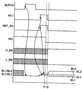
sequence diagram of Figure 1 OB which shows the signal traces and voltage
levels for the
-17-
CA 02692887 2010-02-26
signals shown in the memory array 300 of Figure 8B. It is assumed that anti-
fuse memory
cell 302 is to be accessed during the read operation, and that anti-fuse
memory cell 302 is
unprogrammed. The read operation begins at step 500 where the bitlines are
precharged to
a predetermined voltage level, such as VSS, in response to the rising edge of
BLPCH while
the isolation transistors 306 and 308 are turned on by ISO being at the high
logic level. A
selected wordline WL1 is driven to a read voltage VREAD at step 502, and
repeatedly pulsed
until after time t1, as shown in Figure 10B. The pulse duration, meaning the
amount of time
WL1 is held at VREAD, can be determined by a clock frequency. The pulse
spacing,
meaning the amount of time separating pulses, can also be determined by a
clock frequency.
These parameters of the pulses can be set based on design criteria, such as
the process
technology, the level of VREAD, and the read cycle time for example. This
embodiment is
referred to as a fixed width pulsed wordline scheme.
[0054] Further discussion of different pulse types is discussed later.
[0055] In response to a number of WL1 pulses, a small charge may be added to
BL1 due to
some tunneling current through cell 302. At about the same time at optional
step 504,
reference enable signal REF-EN rises to the high logic level to add a
reference charge to the
unselected bitline BL2. REF_EN can be a reference wordline connected to a
reference cell,
or REF_EN can be a control signal that enables a reference circuit to provide
the charge. As
shown in Figure 10B, BL1/SL1 connected to cell 302 rises slightly above the
VSS precharge
level while BL2/SL2 rises to a reference level higher than BL1/SL1. Following
at step 506,
cell 302 is decoupled from sense amplifier 314 at time t1 by driving ISO to
the low logic level
to turn off isolation transistors 306 and 308. Decoupling is an optional
feature which can be
omitted from the method of Figure 10A. It is noted that BL1 and SL1 remain at
substantially
the same voltage level, as do BL2 and SL2. Later at step 508 the sense
amplifier 314 is
activated (or enabled) by driving H_EN to the high logic level and L_EN to the
low logic level
at time Q. As previously described for the embodiment of Figure 8B and 8C, SL2
and SL1
are driven to high and low voltage levels respectively.
[0056] The pulsed wordline embodiment of Figure 10B uses pulses of equal
duration and
magnitude. According to an alternate embodiment, the pulse widths can vary in
size as
shown in the sequence diagram of Figure 11. The sequence diagram of Figure 11
is identical
to the sequence diagram shown in Figure 10B, except that the pulse
characteristics of WL1
differ from those of WL1 in Figure 10B. In the alternate embodiment of Figure
11, the pulse
widths of WL1 gradually decrease in size (duration) over time. The longer
pulses are used
-18-
CA 02692887 2010-02-26
during the initial activation of the selected wordline WL1 to quickly charge
bitlines connected
to programmed cells. When the time to activate the sense amplifiers
approaches, the pulse
widths should be at their minimum size. For programmed cells, the
corresponding bitlines
should be sufficiently high to sense relative to the reference level. For
unprogrammed cells,
the smaller pulse widths further reduce the duration of time VREAD is applied.
This
embodiment is referred to as a variable width pulsed wordline scheme.
[0057] The pulsed wordline embodiments of Figures 10B and 11 use pulses having
full rail-
to-rail swing, meaning that each pulse rises to the maximum VREAD level, and
then falls to
the VSS level. According to an alternate embodiment shown in Figure 12, all
pulses between
the first pulse and the last pulse fall to an intermediate voltage level that
is above VSS. The
first pulse rises from VSS, but subsequent pulses fall and rise from the
intermediate voltage
level. Only the last pulse falls back to VSS. Thus, WL1 resembles a single
static pulse having
an AC component. This embodiment is referred to as a partial pulsed wordline
scheme,
where the pulse width is constant. This is a variant of the fixed width pulsed
wordline scheme
where the wordline driver is provided with an intermediate voltage above VSS,
instead of
VSS. The advantage of the partial pulsed wordline scheme is that the lower
voltage level of
the wordline WL should be sufficient to charge the corresponding bitline,
while the AC
component peaks will drive any weakly programmed cells. The unprogrammed cells
are not
exposed to a continuous VREAD voltage.
[0058] Further alternate embodiments can include variable magnitude pulses,
where the
initial wordline pulse reaches the maximum VREAD level, followed by successive
pulses with
lower pulse heights. All the described and shown wordline pulsing schemes can
be
combined with each other to form different types of wordline pulses that are
effective for
minimizing the exposure of the unprogrammed cells to VREAD, while ensuring
that
programmed cells can charge their respective bitlines to a level high enough
for sensing
relative to a reference level or the level of an unprogrammed cell for
differential read modes
of operation. The sequence diagrams of Figures 10B, 11 and 12 are shown with
respect to a
read operation executed by the memory array 300 of Figure 8B. These sequence
diagrams
equally apply to a read operation executed by the memory array 400 of Figure
9A, except
that the signal trace for signal PG1 is identical to that of ISO.
[0059] The pulsing of the wordlines according to the previously described
embodiments can
be controlled by controlling wordline drivers, voltage generators, or a
combination of the
-19-
CA 02692887 2010-02-26
wordline drivers and the voltage generators. Figure 13 is a block diagram of a
pulsed
wordline memory, according to a present embodiment.
[0060] The pulsed wordline memory 600 of Figure 13 includes an anti-fuse
memory array
602 having anti-fuse memory cells connected to bitlines (not shown) and
wordlines, such as
wordlines WL1 to WLi, where i is an integer value corresponding to the last
wordline in the
memory array 602. The arrangement of the anti-fuse memory cells, wordlines,
bitlines and
other related circuits can correspond to that previously shown in Figures 8B
or 9A. In the
example of Figure 13, the anti-fuse memory cells are of the single-transistor
type shown in
Figures 4A to 4C. The wordlines are driven by respective wordline drivers 604
to provide at
least the read voltage VREAD and programming voltage VPP. Other voltages can
be driven
onto the wordines by wordline drivers 604. The wordline drivers 604 are
enabled by a
decoded row address signals R_ADD[0] to R ADD[i], where i is the same
previously
described integer value. Row address decoding is well known in the art, and it
should be
understood that during a read or program operation, one of R ADD[0] to
R_ADD[i] is driven
to an active logic level to enable its corresponding wordline driver 604. The
exception to this
decoding scheme is when two wordlines are enabled at the same time for the
differential
read mode of operation.
[0061] A voltage circuit 606 provides VPP, VREAD, VSS and other possible
voltages to the
wordline drivers 604, which is driven onto the wordline when the specific
wordline driver 604
is selected. Voltage circuit 606 can receive voltages such as VDD, VPP and VSS
directly
from voltage supplies externally provided to the memory 600. Alternately,
voltage circuit 606
can include voltage pumps and generators that are well known in the art, for
generating the
VPP voltage, and any other intermediate voltages. Such an intermediate voltage
can be used
for the wordline pulsing scheme of Figure 12. A read/program control signal
RD/PGM is
received to control voltage circuit 606 to selectively provide the proper
voltages during read
and program operations. Voltage circuit 606 outputs a high voltage and a low
voltage to each
of the wordline drivers 604. A pulse control circuit 608 provides pulsing
signals for enabling
and disabling the wordline drivers 604 in a sequence or pattern that results
in any one of the
previously described wordline pulsing schemes. For example, if the wordline
drivers 604 are
enabled and disabled at fixed intervals, then fixed width pulses will result.
Alternately, if the
wordline drivers 604 are enabled and disabled at variable intervals, then
variable width
pulses will result.
-20-
CA 02692887 2010-02-26
[0062] Only the wordline driver enabled by a decoded row address signal
responds to these
enabling signals. The pulse control circuit receives a pulse enable signal
PUL_EN to enable
generation of the pulsing signals during read operations. Pulse enable signal
PUL_EN can
be derived from the read/program signal RD/PGM. The pulsing signals can be
generated in
response to a clock signal, and the pulse control circuit 608 can include
different types of
circuits for generating the previously shown pulsing schemes. For example,
well known clock
dividing or multiplying circuits can be included for generating pulses of
different widths for the
embodiment of Figure 10B. In another example, circuits which can change a duty
cycle of a
clock signal can be used to generate pulses of decreasing width for the
embodiment of
Figure 11. A variety of circuits exist that can be adapted for the present
application.
[0063] Figure 14 is a circuit schematic example of a wordline driver circuit
604 shown in
Figure 13. Wordline driver 604 is shown as a controlled inverter circuit
having p-type
transistors 650, 652 and n-type transistors 654, 656 connected in series
between a high
voltage input VH and a low voltage input VL. High voltage VH is one of the two
voltages
received from voltage circuit 606 of Figure 13, while low voltage VL is the
other of the two
voltages received from voltage circuit 606. The gate of transistor 650
receives high pulsing
signal PH_EN and the gate of transistor 656 receives low pulsing signal PH_EN,
both of
which are the pulsing signals provided by pulse control circuit 608.
Transistors 652 and 654
form a complementary pair, and their gates receive a decoded row address
signal R ADD[n].
The wordline driver circuit shown in Figure 14 is one example of many
different circuit
configurations which can be used.
[0064] In a read operation, VH and VL are provided to the wordline driver 604,
which is
selected when R ADD[i] is driven to the active logic level. Then PH_EN and
PL_EN are
driven between the active and inactive logic levels in a sequence or pattern.
Hence VH and
VL are applied to the wordline WILL The frequency and duration of the active
and inactive
levels of PH_EN and PL EN determine the pulse widths. VH and VL can change
during the
read operation to change the maximum pulse height and the minimum pulse floor.
[0065] The previously described embodiments illustrate techniques for
maximizing retention
of unprogrammed anti-fuse memory cells. The wordlines can be pulsed to
minimize the
exposure of the gate oxides of unprogrammed cells to the read voltage, and the
cells can be
decoupled from sense amplifiers prior to being enabled. Both techniques can
reduce the
amount of tunneling current through the gate oxide of the unprogrammed cells,
while
reducing power consumption.
-21 -
CA 02692887 2010-02-26
[0066] In the preceding description, for purposes of explanation, numerous
details are set
forth in order to provide a thorough understanding of the embodiments of the
invention.
However, it will be apparent to one skilled in the art that these specific
details are not
required in order to practice the invention. In other instances, well-known
electrical structures
and circuits are shown in block diagram form in order not to obscure the
invention. For
example, specific details are not provided as to whether the embodiments of
the invention
described herein are implemented as a software routine, hardware circuit,
firmware, or a
combination thereof.
[0067] Embodiments of the invention can be represented as a software product
stored in a
machine-readable medium (also referred to as a computer-readable medium, a
processor-
readable medium, or a computer usable medium having a computer-readable
program code
embodied therein). The machine-readable medium can be any suitable tangible
medium,
including magnetic, optical, or electrical storage medium including a
diskette, compact disk
read only memory (CD-ROM), memory device (volatile or non-volatile), or
similar storage
mechanism. The machine-readable medium can contain various sets of
instructions, code
sequences, configuration information, or other data, which, when executed,
cause a
processor to perform steps in a method according to an embodiment of the
invention. Those
of ordinary skill in the art will appreciate that other instructions and
operations necessary to
implement the described invention can also be stored on the machine-readable
medium.
Software running from the machine-readable medium can interface with circuitry
to perform
the described tasks.
[0068] The above-described embodiments of the invention are intended to be
examples
only. Alterations, modifications and variations can be effected to the
particular embodiments
by those of skill in the art without departing from the scope of the
invention, which is defined
solely by the claims appended hereto.
-22-