Note: Descriptions are shown in the official language in which they were submitted.
CA 02693059 2010-01-12
WO 2009/012112 PCT/US2008/069638
METHOD AND APPARATUS USING ELECTRIC FIELD FOR IMPROVED
BIOLOGICAL ASSAYS
Inventors: Mostafa Ronaghi, Tarun Khurana, Juan G. Santiago
CROSS-REFERENCE TO RELATED APPLICATIONS
This application claims priority from U.S. Provisional Patent Application No.
60/959,398 filed on July 13, 2007, which is hereby incorporated by reference
in its entirety.
STATEMENT OF GOVERNMENTAL SUPPORT
None.
REFERENCE TO SEQUENCE LISTING, COMPUTER PROGRAM,
OR COMPACT DISK
None
BACKGROUND OF THE INVENTION
Field of the Invention
The present invention relates to the field of biological assays and apparatus
for
carrying out such assays, such as a microfluidic device, to which is applied
electric fields to
control movement of charged molecules. The assays involve charged molecular
species, such
as nucleotides (due to phosphate ions), or other molecules which contain a
charge due to their
ionic nature, such as certain proteins or small molecules.
Related Art
Advances in silicon microfabrication have been used to produce microchannels
and
microarrays for many lab-on-a-chip platforms. Advantages include low reagent
costs,
miniaturization, and fast reaction rates. However, the challenge is to
efficiently isolate and
deposit biological samples into individual wells for high-throughput analysis.
Recently,
random arrays have been implemented in which solid-supports are used to
individually
capture unique biological molecules and deposit these solid supports into
reaction wells with
a geometry of the same size range. Another challenge these platforms are faced
with is when
repetitive assay are performed on the same bead isolated within a well. A good
example
where these challenges are common is DNA sequencing.
1 of 32
CA 02693059 2010-01-12
WO 2009/012112 PCT/US2008/069638
In certain methods of DNA sequencing, DNA is immobilized on a solid support,
and
nucleotides and enzymes are delivered to the DNA for successive incorporation
of
nucleotides. This is commonly referred to as DNA sequencing using sequencing-
by-
synthesis. Nucleotides are removed through washing to allow iterative
nucleotide addition.
One of the main challenges in sequencing by synthesis is to deliver the
nucleotide to the
vicinity of DNA to enable rapid incorporation and to remove the nucleotide
efficiently to
enhance the read-length.
Particular Patents and Publications
Dressman et al., "Transforming single DNA molecules into fluorescent magnetic
particles for detection and enumeration of genetic variations," Proc Nat Acad
Sci July 22,
2003, vol. 100, no. 15,pp 8817-8822, discloses a technique in which each DNA
molecule in a
collection of such molecules is converted into a single magnetic particle to
which thousands
of copies of DNA identical in sequence to the original are bound. Variation
within the
original population of DNA molecules can then be simply assessed by counting
fluorescently
labeled particles via flow cytometry. This approach is called BEAMing on the
basis of four of
its principal components (beads, emulsion, amplification, and magnetics).
After PCR cycling,
the microemulsion is broken by detergent, and the beads are separated from the
oil phase by
centrifugation, and by placing the tube on an MPC-S magnet from Dynal.
Margulies et al., "Genome sequencing in microfabricated high-density picolitre
reactors," Nature 437, 376 - 380 (2005) discloses a method and apparatus for
sequencing by
synthesis which uses open wells of a fiber optic slide. The method uses a
modified
pyrosequencing protocol that is designed to take advantage of the small scale
of the wells.
The fiber optic slides are manufactured by slicing of a fiber optic block that
is obtained by
repeated drawing and fusing of optic fibers. The slide, containing
approximately 1.6 million
wells, is loaded with beads and mounted in a flow chamber designed to create a
300-mm high
channel, above the well openings, through which the sequencing reagents flow.
The unetched
base of the slide is in optical contact with a second fiber optic imaging
bundle bonded to a
charge-coupled device (CCD) sensor, allowing the capture of emitted photons
from the
bottom of each individual well. 800 ml of emulsion containing 1.5 million
beads are prepared
in a standard 2-ml tube. Each emulsion is aliquotted into eight PCR tubes for
amplification.
After PCR, the emulsion is broken to release the beads, which include beads
with amplified,
immobilized DNA template and empty beads.
2 of 32
CA 02693059 2010-01-12
WO 2009/012112 PCT/US2008/069638
The enriched template-carrying beads are deposited by centrifugation into open
wells.
Streptavidin-coated SeraMag beads are bound to the biotinylated enrichment
primers
annealed to the immobilized templates on the DNA capture beads. It is
essential not to vortex
the beads, as vortexing may break the link between the SeraMag and DNA capture
beads.
Erickson et al., "Electrokinetically Based Approach for Single-Nucleotide
Polymorphism Discrimination Using a Microfluidic Device," Anal. Chem., 77
(13), 4000 -
4007, (2005) discloses an electrokinetic approach for single-nucleotide
polymorphism (SNP)
discrimination using a PDMS/glass-based microfluidic chip. The technique takes
advantage
of precise control of the coupled thermal (Joule heating), shear
(electroosmosis), and
electrical (electrophoresis) energies present at an array of probes afforded
by the application
of external electrical potentials. A four-port device is described, with
different voltages
applied to different ports.
Chen et al., "Nanopore sequencing of polynucleotides assisted by a rotating
electric
field," Applied Physics Letters volume 82, number 8, 24 February 2003 1308-
1310 disclose a
method to control the translocation processes of polynucleotides through a
nanopore assisted
by a rotating electric field. Although the work is based on a simulation, it
is stated that the
method can be easily implemented in a nanopore sequencing experiment by adding
two pairs
of parallel electrodes above the thin film.
Erickson, D., Liu, X., Krull, D., Li, D. "An electrokinetically controlled DNA
hybridization microfluidic chip enabling rapid target analysis," Analytical
Chemistry, 2004,
76, 7269-7277, discloses a device in which different voltages are applied to
different ends of
an "H" shaped flow channel. The paper further describes chip fabrication
techniques.
Edman et al., "Electric field directed nucleic acid hybridization on
microchips,"
Nucleic Acids Research, Vo125, Issue 24 4907-4914, discloses a microchip-based
nucleic
acid array where electronic addressing and/or hybridization is carried out by
selective
application of a DC positive bias to the individual microelectrodes beneath
the selected test
sites. This causes rapid transport and concentration of negatively charged
nucleic acid
molecules over selected locations on the microelectronic array. The nucleic
acid (DNA,
RNA, polynucleotides, oligonucleotides, etc.) may then be immobilized by
direct attachment
to the permeation layer overlying the microelectrode or by hybridization to
previously
addressed and attached nucleic acids. This paper describes buffer conditions
and the like
3 of 32
CA 02693059 2010-01-12
WO 2009/012112 PCT/US2008/069638
which may be adapted in practicing the methods taught here. Sosnowski, R.G.,
Tu, E., Butler,
W.F., O'Connell, J.P. and Heller, M.J. Proc. Natl. Acad. Sci. USA, 1997, 94,
1119-1123
(cited in this paper) demonstrates that controlled electric fields can be used
to regulate
transport, concentration, hybridization, and denaturation of single- and
double-stranded
oligonucleotides. Discrimination among oligonucleotide hybrids with widely
varying binding
strengths may be attained by simple adjustment of the electric field strength.
Horejsh et al., "A molecular beacon, bead-based assay for the detection of
nucleic
acids by flow cytometry," Nucleic Acids Res., 2005, 33(2): e13. discloses
another assay
format using beads. In this case, a fluid array system using microsphere-
conjugated molecular
beacons uses a flow cytometer for the specific, multiplexed detection of
unlabelled nucleic
acids in solution. For this array system, molecular beacons are conjugated
with microspheres
using a biotin-streptavidin linkage.
US 6,287,774 to Nikiforov, issued September 11, 2001, entitled "Assay methods
and
system," discloses an assay system comprising a first channel disposed in a
body structure.
The first channel is fluidly connected to a source of a first reagent mixture,
which comprises
a first reagent having a fluorescent label, a source of a second reagent that
reacts with the first
reagent to produce a fluorescently labeled product having a substantially
different charge than
the first reagent; and a source of a polyion. The system also includes a
material transport
system for introducing the first reagent, the second reagent and the polyion
into the first
channel and a detector disposed in sensory communication with the first
channel. The
detector is configured to detect the level of fluorescence polarization of
reagents in the
detection zone.
As referenced in the above patent, a controlled electrokinetic transport
system is
described in detail in U.S. Pat. No. 5,858,195, to Ramsey. Such electrokinetic
material
transport and direction systems include those systems that rely upon the
electrophoretic
mobility of charged species within the electric field applied to the
structure. Such systems are
more particularly referred to as electrophoretic material transport systems.
Other
electrokinetic material direction and transport systems rely upon the
electroosmotic flow of
fluid and material within a channel or chamber structure, which results from
the application
of an electric field across such structures. In brief, when a fluid is placed
into a channel,
which has a surface bearing charged functional groups, e.g., hydroxyl groups
in etched glass
channels or glass microcapillaries, those groups can ionize. In the case of
hydroxyl functional
4 of 32
CA 02693059 2010-01-12
WO 2009/012112 PCT/US2008/069638
groups, this ionization, e.g., at neutral pH, results in the release of
protons from the surface
and into the fluid, creating a concentration of protons at near the
fluid/surface interface, or a
positively charged sheath surrounding the bulk fluid in the channel.
Application of a voltage
gradient across the length of the channel, will cause the proton sheath to
move in the
direction of the voltage drop, i.e., toward the negative electrode.
US 6,733,244 to Fritsch, et al., issued May 11, 2004, entitled "Microfluidics
and small
volume mixing based on redox magnetohydrodynamics methods," discloses a device
where
microfluidic channels utilizing magnetohydrodynamics are used to pump very
small volumes
of solution. The channels have electrodes along the walls of the channel and a
current
carrying species within the solution carries the current through the solution.
The electric field
generated by the use of the current carrying species is perpendicular to a
magnetic field
applied to the channel. The two fields are applied perpendicular to the
desired direction of
flow. The combination of the electric and magnetic fields causes the solution
to flow through
the channel, perpendicular to both fields.
It should be noted that the present devices provide an electric field, which
can move
charged particles (molecules) through a solution. The field does not move the
solution itself.
Furthermore, the field need not be electromagnetic, and does not rely on
ferromagnetic
principles to cause movement. That is, one here is not simply attracting beads
with a magnet.
This would not cause the particle movements described here.
BRIEF SUMMARY OF THE INVENTION
The following brief summary is not intended to include all features and
aspects of the
present invention, nor does it imply that the invention must include all
features and aspects
discussed in this summary.
The present invention relates to the use of an electric-field ("e-field") for
efficient
deposition of charged species, such as beads, molecules (ATP, enzymes), DNA,
and the like,
onto or in the vicinity of an immobilized reactant. The electric field has
been found to be
capable of concentration of substrate and enzyme in the vicinity of DNA
molecule(s) and
efficient nucleotide removal. This technique is implemented in an embodiment
of a
microfluidic device designed for pyrosequencing. The device is designed to
enhance the
overall quality of signals obtained from the light generating reactions and to
improve the
read-length. In particular, we show that one may concentrate or remove
nucleotides near or
5 of 32
CA 02693059 2010-01-12
WO 2009/012112 PCT/US2008/069638
away from beads containing single stranded DNA for enhanced nucleotide
incorporation or
washing. The technique is generally applicable to any charged species that
needs to be
concentrated at or removed from the target site for high throughput analysis.
This technique
uses an AC electric field with DC bias to attract/repel the nucleotides
(charged molecules).
Changing the polarity of DC bias results in the concentration or removal of
nucleotides from
the well containing DNA beads. The bias voltage is generally above about 1V,
but may be up
to a maximum voltage which is limited by dielectric breakdown strength, which
may be -15-
20 V or higher.
In certain embodiments, the invention comprises a device having at least one
fluid
channel and a reaction area defined so as to communicate with the fluid
channel. The reaction
area may be a well, chamber, tube, or other physical area. The reaction area
comprises an
opening or exposure to a fluid channel and a bottom offset from the fluid
channel, the device
being constructed for fluid flow in a direction transverse to reaction area
openings,
comprising: (a) a first electrode adjacent to the bottom; (b) a second
electrode adjacent to the
opening; and (c) a controllable voltage source between the first and second
electrodes which
is controllable to provide an alternating positive charge and a negative
charge to a given
electrode, and a DC bias voltage, whereby charged species in a fluid in a
fluid channel are
directed into or out of the reaction area by an electric field between the
electrodes.
Since the device may be used in sequencing or other reactions where detection
of the
reaction is important, the device may further comprise a reaction sensor
coupled to the
reaction area for detecting reactions in the reaction area. This may be a
photomultiplier tube,
a CCD or other device. Optical fibers may be used for improved detection.
Where the
reaction sensor comprises a fiberoptic faceplate, improved sensitivity and
specificity may be
obtained from each reaction well coupled to the faceplate individually. The
reaction sensor
comprises a CMOS photosensitive element for detecting low levels of light, and
furthermore
for quantitating such levels.
The device may further be described as a microfluidic device comprising a
working
fluid containing beads, wherein the reaction area is a well sized to contain
only one bead. In a
microfluidic device, the reaction areas may be defined in an inert, solid
polymer selected
from the group consisting of photoresist and PDMS. If the beads are negatively
charged, the
present movements are facilitated. These beads may be e.g., polystyrene. The
beads may also
be magnetic.
6 of 32
CA 02693059 2010-01-12
WO 2009/012112 PCT/US2008/069638
In certain embodiments, the electrode adjacent to the bottom is a thin layer
of ITO
(Indium tin oxide), less than about 150 nm thick. This electrode will be
optically transparent
for reaction monitoring by the reaction sensor.
The electrodes preferably comprise a dielectric coating. This has been found
to
prevent corrosion and increase the electric field. The dielectric coating may
be, e.g., one or
more of Parylene poly-p-xylylenes, or silicon oxide, or silicon nitride.
The device may be configured as a disposable device adapted to be attached to
a
separate electronic device, and comprising the appropriate fluid channels and
electrodes, e.g.,
a device for directing charged particle movement in a liquid, wherein said
particles are
directed into a reaction area, comprising: (a) a first electrode coated with a
dielectric material
on one side of the liquid in the reaction area; (b) a second electrode coated
with a dielectric
material on an opposite side of the liquid in the reaction area; (c) a fluid
flow channel
transverse to the reaction area; and (d) connections for a signal generator
for applying both an
AC voltage and a DC voltage to the first electrode and the second electrode,
whereby the
electrodes are constructed and arranged to generate an electric field between
them.
The present invention further comprises a method for moving a charged
molecular
species, as described above, in a microfluidic device, said species moving
into a reaction area
from a fluid channel communicating with the reaction area, comprising the
steps of: (a)
flowing the charged molecular species in the fluid channel in a flow
direction; (b) providing
an electric field having a positive end and a negative end across the reaction
area; and (c) and
directing the charged molecular species into the reaction area by applying a
charge to the
electric field in the reaction area opposite to the charge on the molecular
species. In one
aspect of this embodiment, more than one molecular species is moved into the
reaction area,
thereby causing a reaction between the molecular species. In another aspect,
one or more
molecular species is already in the reaction area, causing a reaction between
the charged
molecular species and the one or more molecular species in the reaction area.
The electric
field contains an AC component at a frequency of at least 100 kHz and,
preferably, a DC bias
voltage, which may be at least 1 Volt, but generally is not of high voltage.
The method may
further comprise the step of reversing the polarity of the DC bias voltage, to
direct the
charged molecular species out of the reaction area.
7 of 32
CA 02693059 2010-01-12
WO 2009/012112 PCT/US2008/069638
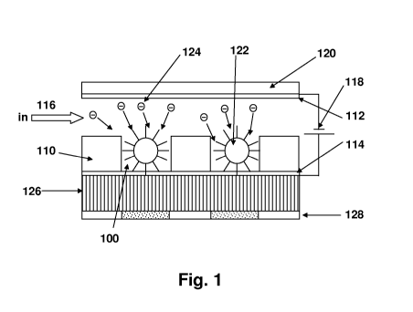
BRIEF DESCRIPTION OF THE DRAWINGS
Figure 1 is a schematic of a device according to the present invention showing
a fiber
optic faceplate with microfabricated wells and ITO electrodes. The negatively
charged
nucleotides can be directed towards the DNA beads by applying a potential
difference across
these electrodes;
Figures 2A and 2B are schematics of the setup for concentrating or removing
nucleotides (or other charged molecules) near the DNA bead (or other target
sites), with an
alternative electrode arrangement shown in Fig. 2B;
Figure 3A and B are photographs showing electric field assisted trapping of 1
m
beads inside 50 m wells. Out of the 4 electrodes shown in the image, voltage
is off (3A)
then applied (3B) at 2 electrodes and stacking of particles is observed at
these sites.
Figure 4 A and B is a schematic drawing (perspective view in 4A and side view
in
4B) of an experimental device used to show concentration of fluorescent dye in
an electric
field;
Figure 5A and B are photographs showing fluorescent dye unconcentrated (5A)
and
concentrated (5B) by an electric field; and
Figure 6 is a graph showing increased chemiluminescence resulting from an
electric
field, which increases pyrophosphate near light generating enzymes in a
reaction area.
DETAILED DESCRIPTION OF THE PREFERRED EMBODIMENT
Definitions
Unless defined otherwise, all technical and scientific terms used herein have
the same
meaning as commonly understood by those of ordinary skill in the art to which
this invention
belongs. Although any methods and materials similar or equivalent to those
described herein
can be used in the practice or testing of the present invention, the preferred
methods and
materials are described. Generally, nomenclatures utilized in connection with
biochemistry
and biophysics as used here are those well known and commonly used in the art.
Certain
experimental techniques, not specifically defined, are generally performed
according to
conventional methods well known in the art and as described in various general
and more
specific references that are cited and discussed throughout the present
specification. For the
n rnn-,P-, c)f r1a,-;tv t1,P following terms are defined below.
8 of 32
CA 02693059 2010-01-12
WO 2009/012112 PCT/US2008/069638
The term "microfluidic device" is used in a conventional sense, it being
understood
that the present device is preferred for use and is advantageous with small
reaction volumes
and liquid flow rates. In general, the reaction wells should be no larger than
100 nL and may
be as small as 1 pL. In a preferred embodiment described below, they are 35 m
in diameter.
The device will include liquid flow channels for flowing buffer and reactants
into the reaction
wells. The reaction wells may be sized to hold a single charged bead. The
reaction wells are
generally any defined space where reactants are brought together and are
located out of the
direct flow of the fluid channel unless the device is configured to direct the
reactants into the
reaction area, or out of the reaction area, by charging the electrodes to
provide a field
attracting or repelling the charged species into or out of the well.
The term "transverse" is used in a general sense to mean crosswise,
preferably, but
not necessarily, perpendicular.
The term "electric field" is used to mean the effect produced by the existence
of an
electric charge, such as an electron, ion, or proton, in the volume of space
or medium that
surrounds it. Each of a distribution of charges contributes to the whole field
at a point on the
basis of superposition. A charge placed in the volume of space or in the
surrounding medium
has a force exerted on it. Electric fields are created by differences in
voltage: the higher the
voltage, the stronger will be the resultant field. In contrast, magnetic
fields are created when
electric current flows: the greater the current, the stronger the magnetic
field. An electric field
will exist even when there is no current flowing. Electric fields are measured
in Volts per
meter (V/m). In order to cause movement of the charged particles in the
present methods and
device, within a convenient time frame, the electric field strength should be
about 5 V/cm or
higher, up to practical limits of Joule heating and dielectric breakdown
limits, with the
maximum upper value being about 1000 V/cm
As an example of a high strength electric field, it is noted that water, being
dipolar,
can be partly aligned by an electric field and this may be easily shown by the
movement of a
stream of water by an electrostatic source. Very high field strengths (5 x 10⁹
V rri i) reorient
water in ice such that freezing is inhibited.
General method and Apparatus
Described below are apparatus and methods for electric field directed
concentration
and washing of charged molecules.
9 of 32
CA 02693059 2010-01-12
WO 2009/012112 PCT/US2008/069638
Previous electrophoretic concentration techniques have relied on faradaic
current to
concentrate the charged species at the electrode site. This typically results
in electrolytic
reactions occurring at the electrodes and generation of electrolysis products
such as oxygen
and hydrogen. The present method uses a displacement field through capacitive
coupling of
the electrodes rather than faradaic current through the electrodes.
The electric field used herein is based on accepted principles of capacitance.
When
two plates of different charge are placed near each other, as in a parallel
plate capacitor, the
two E-fields between the plates add while the E-fields outside the plates
cancel. When the
plates are close to each other to form a capacitor, the E-field between the
plates is constant
throughout the interior of the capacitor as long as one is not near the edges
of the plates.
Since the electric field is the negative of the gradient of the potential and
the E-field is
constant inside a capacitor, the magnitude of the electric field E has a very
simple relation to
the voltage V between the plates and their separation d.
E,_V
d
Equation 1
By placing a thin insulating material (a dielectric) between the plates the
separation d
can be reduced thus increasing the capacitance of the capacitor and preventing
the plates from
touching.
Displacement current is a quantity related to a changing electric field. It
occurs in
dielectric materials and also in free space.
The displacement current is mathematically defined by the rate of change of
the
electric displacement field, (a known physics term, also called electrical
field/flux density) D:
JD = aD aE
-=~-
at at
Equation 2
where D = EE where the permittivity E= Eo Er, and where
= Er is the relative permittivity of the dielectric and
= Eo is the permittivity of free space ( 8.854 E-12 Frri i).
10of32
CA 02693059 2010-01-12
WO 2009/012112 PCT/US2008/069638
In the present device, in response to the applied DC voltage across the
electrodes, electric
double layers are created at the electrodes that shield the voltage applied at
the electrodes.
Hence, a DC voltage across the electrodes does not result in an electric field
in the bulk of the
channel due to shielding by electric double layers, and faradaic current is
necessary to
achieve concentration. However, if the voltage across the electrodes is
switched at a time
scale faster than the time taken by ions to form the double layers, the effect
of shielding
becomes negligible and an electric field exists across the entire channel
width. The AC
frequency required for a typical case of 10 mM ionic strength electrolyte with
10 nm thick
dielectric layer and gap between electrodes of - 100 m is - 100 kHz. The
present method
uses alternating fields, changing at frequency -500 kHz or higher, with a net
DC bias to
achieve a net electric field across the electrodes without any faradaic
current.
If one were to apply across the fluid flow channel a DC voltage by itself, the
voltage
near one surface of the channel would be shielded by an electric double layer
within about
lOnm from the channel wall. The electric field would thus be largely zero
throughout the
remaining width of the channel (beyond -10 nm from that wall). If one were to
apply only
AC voltage, which is switched faster than the response time of the ions (-
0.lms), the effect of
the electric field would be applied equally across the entire channel.
However, the average
electric field would still be zero. In the case of both DC and AC voltage,
there is a time
averaged DC field across the entire channel, resulting in a force E, which is
high at one side
of the channel and decreases with the distance from that side.
By way of further explanation, it may be said (without wishing to be bound by
any
theory) that the present methods and devices employ a particular type of
electrokinesis.
Electrokinesis refers to a class of phenomena elicited by the action of an
electric field on the
mobile ions surrounding charged objects in an electrolyte solution. When an
object of given
surface charge is immersed in a solution containing ions, a diffuse ion cloud
forms to screen
the object's surface charge. This arrangement of a screening cloud of
(immobile) charges
associated with an immersed object and a layer of (mobile) counterions in
solution is referred
to as a "double layer". In this region of small but finite thickness, the
fluid is not
electroneutral. Consequently, electric fields acting on this region will set
in motion ions in the
diffuse layer, and these will in turn entrain the surrounding fluid. The
resulting flow fields
reflect the spatial distribution of ionic current in the fluid. Electroosmosis
represents the
simplest example of an electrokinetic phenomenon. It arises when an electric
field is applied
11 of 32
CA 02693059 2010-01-12
WO 2009/012112 PCT/US2008/069638
parallel to the surface of a sample container or electrode exhibiting fixed
surface charges, as
in the case of a silicon oxide electrode (in the range of neutral pH). As
counterions in the
electrode double layer are accelerated by the electric field, they drag along
solvent molecules
and set up bulk fluid flow. This effect can be very substantial in narrow
capillaries and may
be used to advantage to devise fluid pumping systems.
Electrophoresis is a related phenomenon, which refers to the field-induced
transport
of charged particles immersed in an electrolyte. As with electroosmosis, an
electric field
accelerates mobile ions in the double layer of the particle. If, in contrast
to the earlier case,
the particle itself is mobile, it will compensate for this field-induced
motion of ions (and the
resulting ionic current) by moving in the opposite direction. Electrophoresis
generally is
carried out in a gel or medium with a solid mesh, which will retard the ionic
particles
according to a certain basis, e.g., size. As described below, it is
contemplated here that the
particles will be in a liquid fluid without impeding gels or solid phase.
Referring now to Figure 1, there is illustrated a microfluidic device having
wells 100
defined in a layer of SU-8 photoresist 110, which device further comprises an
electrode 112
spaced above the layer 110 and extending between the wells so as to define a
fluid flow
channel (as shown at 116) between the electrode 112 and the photoresist layer
110 and
communicating with the wells. The fluid channel is preferably on the order of
100 m deep,
in that the present device is particularly well suited for 10 L volumes. The
layer 110 is a
well forming layer (i.e., a layer patterned to define at least a part of the
reaction areas and a
fluid flow channel). The layer is defined from photoresist for ease of
fabrication at a
submicron scale. It is preferred that a high aspect ratio (e.g., d/w > 5:1) be
achieved in the
well. In other words, the reaction area or well is offset from the channel (by
the etching) to a
certain depth and is a cavity of a certain (relatively narrow) width or
diameter. Beads may
flow through the fluid flow channel and into wells. A second electrode 114 is
under the well
forming layer 110 to define a bottom portion of a well. Where wells have been
formed
(etched or molded) in the layer, the electrode is exposed to the fluid and
materials in the well,
which enters the device as shown at arrow 116. Electrodes 112 and 114 are
preferably formed
of ITO (indium tin oxide) approximately 100 nm thick. As further shown in
Figure 1, these
electrodes form essentially parallel sheets, with the fluid channel and the
wells in between.
It is important to note that a dielectric layer made of silicon oxide or
parylene or
silicon nitride of - 100 nm thickness is applied to the electrodes, e.g.,
above the ITO layer, as
12 of 32
CA 02693059 2010-01-12
WO 2009/012112 PCT/US2008/069638
shown in Figure 2 (204 and 206). Further as shown in Figure 1 and Figure. 2A
and B, a
voltage source 118 (Figure 1) connects the electrodes and is charged such
that, as will be
described in detail below, the top electrode 112 is negative and the bottom
electrode 114 (at
the bottom of the wells) is positive, in order to drive particles (atoms,
molecules, beads, etc.)
into the wells. The terms "top" and "bottom" are used here for convenience,
and the device
may be configured in various orientations with regard to gravity or
orientation in use.
Referring again to Fig. 1, the top electrode 112 is applied to a substrate
120, which is
made e.g., of borosilicate glass or quartz and is spaced above the well
forming layer 110 by
any etched or machined structure, such as a step in the photoresist layer.
In an exemplary method, beads 122 containing DNA molecules bound to the
surface
and extending outwardly are shown as being contained in the wells 100 (one
bead per well).
Oligonucleotides are attached to the beads as is known in the art (see related
patents and
publications). The beads have been delivered to the well area by fluid flow
116 and assisted
in entering wells by the electric field achieved by electrodes 112 and 114
above and below
the well, or by magnets. An electric field is applied to drive negatively
charged molecules
such as shown at 124 towards the beads and into the well. The molecules may be
nucleotides,
enzymes, or other charged species. The molecules are delivered in a suitable
buffer and cause
a detectible reaction with the DNA strands on the beads. Low concentration (-
10 mM) Tris-
Acetate or Tris HCI are preferred for use as the buffer.
In one embodiment, the charged molecules are nucleotides which are
incorporated
into a polynucleotide and generate, in the reaction area, inorganic
phosphorous, which is used
to generate a detectible light signal (e.g., pyrosequencing). Accordingly, a
fiber optic
faceplate 126 is attached to a thin, transparent electrode 114, which, with
any dielectric
coating, forms the bottom of the reaction area. The electrode is transparent
to the light to be
collected. The fiber optic faceplate 126 may be from a commercially available
source, e.g.,
Schott North America, Inc. The fiber optic faceplate is composed of a bundle
of fused fibers
aligned in parallel and perpendicular to the bottom surface of well 100. In
this way, light is
efficiently transmitted from each individual well 100 to a light sensor, such
as a CMOS
sensor 128 coupled to the fiber optic faceplate with sensing areas under each
well. As is
known, CMOS, which stands for Complementary Metal Oxide Semiconductor, imagers
include an array of photo-sensitive diodes, one diode within each pixel.
Unlike CCDs,
however, each pixel in a CMOS imager has its own individual amplifier
integrated inside.
13 of 32
CA 02693059 2010-01-12
WO 2009/012112 PCT/US2008/069638
Since each pixel has its own amplifier, the pixel is referred to as an "active
pixel". The shaded
areas in CMOS detector 128 are aligned with individual wells and receive the
maximum light
from that well, and only light from that well. Each well is coupled to an
individual CMOS
detector element.
To take advantage of the full capacity of the CMOS pixels and achieve the best
possible coverage, which is essential for improving system throughput, the
device is
constructed with a near perfect alignment of the wells 100 with the CMOS
sensor pixels.
This, however, cannot be achieved with alignment of the fibers in the
faceplate with the
pixels because of the irregularities of the patterns in available fiber
faceplates. The most
convenient way to avoid direct alignment is to use optical fibers, which are
much smaller in
dimension as compared to the wells and the CMOS pixels. Using such a faceplate
circumvents the problem of alignment of the faceplate to the pixel and wells.
The pixel and
the wells, however, do need to be aligned. This can very easily be done by
fixing the image
sensor position and using two micrometer adjusters in the X and Y dimensions
to get perfect
alignment of the microfluidic platform containing the wells. This process can
either be done
by hand or through a more complicated stepper motor mechanism. The calibration
metric
used to detect perfect alignment can be set as the amount of collective
photocharge across the
entire image sensor area in presence of a calibrated amount of ATP or PPi
assay before each
run. If not well aligned, the light signal can be lost on the area between the
individual CMOS
pixels, but as alignment gets better, the lost photon flux diminishes. Maximum
light intensity
indicates perfect alignment. Automatic adjustment of the microfluidic and CMOS
sensor
plates can be achieved through application of piezoelectric actuation. In this
technique, the
microfluidic plate holder will be equipped with a single or multiple
piezoelectric actuators.
Once the plate is inserted in the holder, the piezoelectric actuator can be
activated with a
feedback from the CMOS output to move the plate to a single position each
time. Our
calculations indicate that 2N of force should be sufficient for moving the
plates toward
alignment. Piezoelectric actuators capable of such forces are commercially
available. It has
also been shown that alignment within ms can be achieved using such a
technique. The best
position for the wells, in terms of light efficiency, would be as close to the
faceplate as
possible. Therefore our wells are fabricated right on top of the faceplate
through deposition
and patterning a layer of SU-8 on top of the faceplate. Based on our
simulations, the optical
efficiency can be greatly improved by this direct coupling from 1.6% to more
than 90%.
14of32
CA 02693059 2010-01-12
WO 2009/012112 PCT/US2008/069638
A schematic drawing further showing aspects of the present device and
technique is
shown in Figure 2A. In this embodiment, there is shown an indium tin oxide
(ITO) electrode
material coated (-150 nm thick) (112 and 114, as in Figure. 1) onto standard
glass slides 200,
202 to apply the electric field in the channel, traverse to the direction of
flow. The transparent
ITO electrodes are further coated with a thin layer (-20 nm) of dielectric
204, 206 such as
Parylene or silicon oxide or silicon nitride (shown as patterned in Figure. 2)
to prevent
corrosion of the electrode due to electrolysis and to facilitate the electric
displacement field.
Thus, the fluid channel has one surface coated with a dielectric layer, which
is in contact with
the fluid, and an opposing surface, bearing electrode portions, where the
electrode portions
are also coated with a dielectric layer. Parylene is a generic term applied to
the family of
unsubstituted and substituted. Parylene N and SCS Parylene HT have
particularly high
dielectric strength, and a dielectric constant independent of frequency, and
may be preferred.
Further description of Parylene dielectric materials is found in US 4,163,828
to Mahoney,
issued August 7, 1979, entitled "Parylene stabilization."
In Figure 2B a variation of an electrode array is shown. In this embodiment, a
glass
layer such as shown at 202 in Figure 2A is adapted for a CMOS fabrication
process in which
a CMOS sensor is placed directly below the well and under a transparent layer
117. The well
electrodes are preferably coated by a dielectric layer (not shown), but are
formed out of one
or both of a series of wires 115, 115a, or electrode strips 119 under the well
forming layer,
and along the sides of the well, at the bottom portion. In top view, the wires
and electrodes
would be in the form of a grid, forming a square around each well, at the
bottom portion, near
the sensor. This would allow the fabrication of wells with electrodes on the
order of size of
CMOS sensor pixels. If each well (pixel) was 20 M square, for example, a
single or double
wire, with a wire diameter of about 1 M can be used to create a grid and
pulsed to provide
an AC and DC charge. The wires run adjacent to the bottom of the well. Also,
an electrode
can be placed within the side wall of the well, extending partially into the
bottom of the well,
as shown at 115 and 115a. Again, if one considers a "pixel" to be a portion of
the bottom of
the well, which is in optical contact with a sensor, the pixel is bounded on
four sides by an
electrode, in this case, a set of metal strips, where each strip is mostly
within the sidewall of
the well, but extends somewhat into the bottom of the well. These metal wires
115 and metal
strips 119 are connected to the voltage source and operated as described
above.
15 of 32
CA 02693059 2010-01-12
WO 2009/012112 PCT/US2008/069638
The flow structure containing the flow channel and the wells for DNA beads is
fabricated in SU-8 (- 200 m thick). PDMS/silicone gaskets can also be used to
create the
flow channels. The ITO-dielectric coated glass slides form the top and the
bottom layer of the
flow channel. As described in connection with Figure 1, a bead 122 is in a
well in a fluid
medium containing charged particles 124, and a voltage source connects the
electrodes so as
to cause movement of the particles towards or away from the well and the bead
122 in the
well, the bead having attached to it reactants such as oligonucleotides for
reaction with
nucleotides 124.
Conventional photolithography techniques can be applied for SU-8 patterning.
Such
fabrication processes for SU-8 have already been tested and verified at the
Stanford
nanofabrication facility. The SU-8 processing allows fabrication of high
aspect-ratio wells,
which is critical for reducing chemical crosstalk between adjacent beads. That
is, the reaction
area should completely contain the bead.
Given the above description of the preferred embodiment of the present device,
it will
be apparent that a variety of alternative constructions are possible. Although
not illustrated, it
can be envisioned that in one embodiment, each well may be coupled to an
individually
controlled electrode pair, and different wells may be in different states of
charged species
attraction or repulsion at the same time.
The electrodes may be made of a variety of transparent electrically-conductive
layers,
such as metal oxides such as indium tin oxide (ITO), antimony doped tin oxide,
and cadmium
stannate (cadmium tin oxide), each of which is commonly used as transparent
electrodes in
electro-optical devices such as liquid crystal displays. The electrodes are
transparent for
purposes of optical detection. In devices where the reaction is measured
thermally or
electrically, the electrodes do not need to be transparent. For example, the
device may be
used for electrical detection of a binding reaction. See, US 5,284,748 to
Mroczkowski, et al.
February 8, 1994, entitled "Method for electrical detection of a binding
reaction." A
voltametric immunoassay can be carried out by labeling one immunoreactant with
an
electroactive substance. Pace U.S. Pat. No. 4,233,144, issued Nov. 11, 1980,
is illustrative of
one such technique. Another method involves sandwiching an antigen-antibody
layer
between two conductive layers and measuring the electrical capacitance of the
resulting
laminate. Giaever U.S. Pat. No. 4,054,646, issued Oct. 18, 1977, describes
such a method. A
further type of capacitance-measuring system includes a pair of electrodes
coated with a
16of32
CA 02693059 2010-01-12
WO 2009/012112 PCT/US2008/069638
substrate and immersed in a medium containing a material which specifically
binds with the
substrate, as described in Arwin U.S. Pat. No. 4,072,576.
The well-forming layer may be formed of any inert material. Photolithographic
techniques may be employed to pattern the layer into a series of fluid
channels and reaction
areas, for example as described in US 6,960,437 to Enzelberger, et al., issued
November 1,
2005, entitled "Nucleic acid amplification utilizing microfluidic devices." As
described there,
microfluidic devices are constructed at least in part from elastomeric
materials and
constructed by single and multilayer soft lithography (MLSL) techniques and/or
sacrificial-
layer encapsulation methods (see, e.g., Unger et al. (2000) Science 288:113-
116, and PCT
Publication WO 01/01025) Utilizing such methods, microfluidic devices can be
designed in
which solution flow through flow channels of the device is controlled, at
least in part, with
one or more control channels that are separated from the flow channel by an
elastomeric
membrane or segment. More specifically, certain fabrication methods involve
initially
fabricating mother molds for top layers (elastomeric layer with the control
channels) and
bottom layers (elastomeric layer with the flow channel) on silicon wafers by
photolithography with photoresist (Shipley SJR 5740). Channel heights can be
controlled
precisely by the spin coating rate. Photoresist channels are formed by
exposing the
photoresist to UV light followed by development. Heat reflow process and
protection
treatment is performed as described previously (M. A. Unger, H.-P. Chou, T.
Throsen, A.
Scherer and S. R. Quake, Science 288, 113 (2000)).
The photoresist material may be spin or spray-coated onto a substrate such as
a silicon
wafer or applied as a film or web to the wafer. Commercially available dry
film photoresist
materials include acrylic based materials, such as a material available from
Mitsui of Japan
under the trade name Ordyl PR132, epoxy based materials, such as a material
available from
E. I. DuPont de Nemours and Company Corporation of Wilmington, Del. under the
trade
name RISTON, or a material available from MicroChem Corporation of Newton,
Mass.
under the trade name SU-8, (or such as a proprietary material internally used
at Lexmark
International, Inc. of Lexington, Ky. and referred to internally as GSP920),
and polyimide-
based photoresist materials, such as a material available from HD Microsystems
of Parlin,
N.J. under the trade name HD4000.
After applying the photoresist material to the fluid side of a wafer
substrate, the
photoresist material is exposed, as through a mask, to actinic radiation, such
as ultraviolet
17 of 32
CA 02693059 2010-01-12
WO 2009/012112 PCT/US2008/069638
(UV) light to pattern the photoresist material to provide locations for fluid
flow channels in
the photoresist material upon developing the photoresist material. The
patterned photoresist
material is then developed by dissolving uncured material from the fluid
channel/well areas
of the wafer using a developing chemical. The developing chemicals may be
selected from
tetramethyl ammonium hydroxide, xylene or aliphatic hydrocarbons, sodium
carbonate, and
2-butyl cellosolve acetate (BCA). For further details, see US 7,043,838 to
Smoot, et al.,
issued May 16, 2006, entitled "Process for manufacturing a micro-fluid
ejection device."
A general assay protocol for nucleotide preconcentration/washing is as
follows:
1. The flow channel is first filled with the DNA beads.
2. The flow channel is sealed from the top with the ITO-dielectric glass
slide.
3. The flow channel is subsequently filled with the solution containing the
nucleotides.
4. The ITO electrodes are connected to a high frequency AC source and a high
frequency square pulse (Vpeak -5 - 7 V. >100 kHz) is applied across the
channel.
That is, the voltage source 118 provides an AC field to electrodes 112, 114,
electrode
114 being effective only in well bottoms. The AC field is in the range of 2 to
20 volts,
preferably 5 to 7 V, and at a frequency preferably greater than 100kHz, in a
range of
about 10 kHz to about 10 MHz.
This high frequency AC field nullifies the effect of the electric double layer
that forms
at the electrode-liquid interface. In the absence of the AC field, the
electric double
layer would shield the DC voltage applied across the electrodes and there
would be no
DC electric field inside the channel.
5. A small DC voltage (-1.5 V) is superimposed on the existing AC voltage,
again from
voltage source 118. Depending on the polarity of the DC field, the nucleotides
either
concentrate near the DNA beads or are repelled away from the DNA beads in the
wells.
The present device may be used for a wide variety of assays. Preferred assays
include
those that involve transport of nucleotides. These include:
18 of 32
CA 02693059 2010-01-12
WO 2009/012112 PCT/US2008/069638
Primer elon¾ation/de¾radation assay
In this assay, terminal transferase activity is detected in protein
preparations by
incorporation of dATP into ssDNA. A typical procedure involves: 130 nM TdTS or
130 nM
TdTL is incubated at 35 C in 200 nM potassium cacodylate, 25 mM Tris-HC1, pH
6.6, 0.25
mg/ml BSA, 4 mM MgC12, 4 M ZnSO4, 5 Io glycerol, 1 mM dATP, and 20 nM 5'-32P-
labeled (dA) 10 primer. The 3'5' exonuclease activity in protein preparations
are searched
using the same assay in the absence of dATP. Aliquots are withdrawn at 0, 5,
15, 30, and 60
min, supplemented with a formamide dye mix, and electrophoresed on a 16%
acrylamide
denaturating gel. Products are visualized after exposure of the wet gel under
a Kodak film
(Biomax MR) at -70 C. See The Journal of Immunology, 2004, 172: 6764-6767.
"Evidence
That the Long Murine Terminal Deoxynucleotidyltransferase Isoform Plays No
Role in the
Control of V(D)J Junctional Diversity."
Clonal analysis of DNA, or Multiplex Analysis
This assay uses a device having a plurality of reaction areas, where each
reaction area
is a well designed to hold one, and only one, bead. DNA molecules are attached
to neutrally
charged beads using methods known in the art, with one species of DNA for each
bead.
Examples of neutral materials that may be used for the bead include glass,
polyacrylamide,
polystyrene, Sepharose beads (crosslinked polysaccharide agarose, trademark
of GE
Healthcare. Properties), other forms of agarose, latex, etc. In addition,
magnetic beads may be
used, as illustrated in Example 3. Because the process of attaching DNA or
other molecules is
imperfect, this will result in two populations of beads, one population with
DNA, and one
population without DNA. Both populations are put in the flow channel, and an
AC field with
DC bias is applied to the wells. Because DNA is negatively charged, this will
result in DNA-
containing beads being captured in the wells, with naked beads flowing through
such that
they are washed away. This results in an enriched population of DNA-coated
beads in the
device. The DNA on the beads may then be amplified, using techniques known in
the art. The
DNA-coated beads may be a variety of known bead materials and connected
directly to
oligonucleotides or polynucleotides of DNA (or RNA), which are then processed
further,
either by acting as sequencing templates, by acting as probes for the
attachment of other
polynucleotides, or the like. The beads may be coated with streptavidin and
attached to
biotinylated DNA/RNA, or configured in a wide variety of ways known to those
in the art.
19of32
CA 02693059 2010-01-12
WO 2009/012112 PCT/US2008/069638
In one aspect of this embodiment, the beads are coded with a barcode. A bar
code is a
specific tag that is used to uniquely detect a molecule. The bar code may be
any type of bar
code known in the art, including but not limited to optical tags, fluorescent
tags, electrically
responsive tags, and a set of tags with different masses. The bar codes are
decoded using a
method that depends on the type of barcode, including but not limited to mass,
electrical,
visual, fluorescence, and nucleic acid detection. In this way, the sequence of
DNA in each
reaction area can be identified.
Thus, this method allows for introduction into the flow channel of a
population of
beads, only some of which contain molecules to be analyzed (e.g., DNA),
wherein the beads
containing molecules contain different molecular species (e.g., different DNA
sequences,
different proteins or the like). The beads are put randomly into wells, and
identified by bar
coding. The molecules need only be responsive to the present E-field. As shown
in Fig. 5,
even certain dyes are responsive, as well as proteins and nucleic acids (DNA,
RNA).
Multiplex analysis is carried out in a number of wells, which may be on the
order of
hundreds or thousands of different wells. One may address each well (or a
subset of wells)
with a different fluid channel. Once the target molecules are directed into
individual wells,
reactants are specifically addressed to those molecules for chemical analysis.
The results are
read as described above, and analysis may further includes deconvoluting a bar
code to
identify the target molecule. The term "bar code" is used here loosely to
refer to a unique
molecule (such as an oligonucleotide or magnetic particle) that is associated
with the target
molecule, either directly or through a solid support such as a bead. Further
details may be
found, e.g., in US 6,261,782 to Lizardi, et al., issued July 17, 2001,
entitled, "Fixed address
analysis of sequence tags." Other labels that can be used according to the
present method
include molecular or metal barcodes, mass labels, and labels detectable by
nuclear magnetic
resonance, electron paramagnetic resonance, surface enhanced raman scattering,
surface
plasmon resonance, fluorescence, phosphorescence, chemiluminescence, resonance
raman,
microwave, or a combination. Mass labels are compounds or moieties that have,
or which
give the labeled component, a distinctive mass signature in mass spectroscopy.
Mass labels
are useful when mass spectroscopy is used for detection. Preferred mass labels
are peptide
nucleic acids and carbohydrates. Combinations of labels can also be useful.
For example,
color-encoded microbeads having, for example, 265 unique combinations of
labels, are useful
20 of 32
CA 02693059 2010-01-12
WO 2009/012112 PCT/US2008/069638
for distinguishing numerous components. For example, 256 different ligator-
detectors can be
uniquely labeled and detected allowing multiplexing and automation of the
disclosed method.
Polymerase chain reaction
This standard assay detects the presence of a defined sequence in a DNA
molecule,
which is complementary to a pair of oligonucleotide primers. By adding heating
elements,
PCR reactions may be carried out in a device such as illustrated in Figure. 1.
PCR is
described, for example in basic patents such as U.S. Pat. Nos. 4,683,202;
4,683,195;
4,800,159; and 4,965,188. US 5,512,462 to Cheng, issued Apri130, 1996,
entitled "Methods
and reagents for the polymerase chain reaction amplification of long DNA
sequences,"
describes methods and reagents for the amplification of DNA sequences longer
than 10
kilobases by the polymerase chain reaction (PCR). The methods use compositions
consisting
of a primary thermostable DNA polymerase from Thermus thermophilus combined
with a
lesser amount of a secondary thermostable DNA polymerase possessing a 3'-to-5'
exonuclease activity from Thermococcus litoralis, Pyrococcus species GB-D or
Thermotoga
maritime.
The present methods may also be applied to various methods of DNA sequencing-
by-
synthesis.
Pyrosequencing
The pyrophosphate method described here is a type of sequencing by synthesis
See
Ronaghi et al., "A Sequencing Method Based on Real-Time Pyrophosphate,"
Science, 281:
363 365 (1998) and Hyman, "A New Method of Sequencing DNA," Anal. Biochem.,
174:
423 436 (1988).
As described in Ronaghi, "Pyrosequencing Sheds Light on DNA Sequencing,"
Genome Research Vol. 11, Issue 1, 3-11, January 2001, pyrosequencing is a DNA
sequencing technique that is based on the detection of released pyrophosphate
(PPi) during
DNA synthesis. In a cascade of enzymatic reactions, visible light is generated
that is
proportional to the number of incorporated nucleotides. The cascade starts
with a nucleic acid
polymerization reaction in which inorganic PPi is released as a result of
nucleotide
incorporation by polymerase. The released PPi is subsequently converted to ATP
by ATP
sulfurylase, which provides the energy to luciferase to oxidize luciferin and
generate light.
Because the added nucleotide is known, the sequence of the template can be
determined. The
rõ~iA;~ a~;,a mnlanniA ~an be either RNA or DNA. However, because DNA
polymerases
21 of 32
CA 02693059 2010-01-12
WO 2009/012112 PCT/US2008/069638
show higher catalytic activity than RNA polymerases for limited nucleotide
extension, efforts
have been focused on the use of a primed DNA template for pyrosequencing.
Standard
pyrosequencing uses the Klenow fragment of Escherichia coli DNA Pol I, which
is a
relatively slow polymerase. The ATP sulfurylase used in pyrosequencing is a
recombinant
version from the yeast Saccharomyces cerevisiae and the luciferase is from the
American
firefly Photinus pyralis. The overall reaction from polymerization to light
detection takes
place within 3-4 sec at room temperature. One pmol of DNA in a pyrosequencing
reaction
yields 6 x 10¹¹ ATP molecules, which, in turn, generate more than 6 x
109photons at a
wavelength of 560 nanometers. This amount of light is easily detected by a
photodiode,
photomultiplier tube, or a charge-coupled device (CCD) camera. There are two
different
pyrosequencing strategies: solid-phase pyrosequencing (Ronaghi et al. 1996)
and liquid-
phase pyrosequencing. Solid-phase pyrosequencing utilizes immobilized DNA in
the three-
enzyme system described previously. In this system a washing step is performed
to remove
the excess substrate after each nucleotide addition. In liquid-phase
pyrosequencing apyrase, a
nucleotide-degrading enzyme from potato, is introduced to make a four-enzyme
system.
Addition of this enzyme eliminates the need for solid support and intermediate
washing
thereby enabling the pyrosequencing reaction to be performed in a single tube.
While being advantageous in using native nucleotides, the pyrophosphate method
requires synchronization of polymerases on the DNA strands, which has been
known to
restrict sequence read lengths. Also, it is not expected that the detection
method can approach
single molecule sensitivity due to limited quantum efficiency of light
production by luciferase
in the procedure. Furthermore, the overall sequencing speed is limited by the
necessary
washing steps, subsequent chemical steps in order to identify pyrophosphate
presence, and by
the inherent time required to test each base pair to be sequenced with all the
four bases
sequentially. Also, difficulties in accurately determining homonucleotide
stretches in the
sequences were recognized.
The present methods using electrokinesis of DNA, nucleotides, PPi and the
enzymes
listed above provide significant improvements in pyrosequencing. The reactants
flow into the
wells better, addressing the above-listed potentially problematic areas of
synchronization,
read lengths, and speed.
22 of 32
CA 02693059 2010-01-12
WO 2009/012112 PCT/US2008/069638
Primer extension
As described in US 6,613,513 to Parce, et al., issued September 2, 2003,
entitled
"Sequencing by incorporation," methods of sequencing by synthesis or
incorporation
generally all involve the addition of nucleotides or nucleotide analogs to
reaction mixtures
comprising nucleic acid templates and primers, e.g., DNA or RNA. The
nucleotides are
incorporated into the primer, resulting in an extended primer. The sequence is
determined as
each additional complementary nucleotide is incorporated into the primer and
the steps are
repeated until the entire template sequence or a portion thereof is
determined.
In one embodiment of this method, the nucleotides or nucleotide analogs, or a
fraction
thereof, comprise a 3'-blocking group and a detectable label moiety, which
typically
comprises a phosphate or a carbamate group. The 3'-blocking groups provide
reversible chain
termination. When added to a growing nucleic acid chain, these nucleotide
analogs result in a
non-extendable primer. The 3'-blocking group is typically removed, e.g., by a
reducing agent
and/or a phosphatase, to produce an extendable primer to which further
nucleotides are
added, thereby allowing continued sequencing of the nucleic acid template.
Removal of the
3'-blocking group is optionally performed before or after detection of the
added nucleotide.
In another embodiment of this method, the nucleotides or nucleotide analogs
comprise
a fluorescent label. Sequencing by synthesis using fluorescent nucleotides
typically involves
photobleaching the fluorescent label after detecting an added nucleotide.
Photobleaching
comprises applying a light pulse that destroys or reduces to an acceptable
level, e.g., a
background level or to a low enough level to prevent signal buildup over
several sequencing
cycles, the fluorescence of the nucleotides, e.g., a fluorescent nucleotide
that has been added
to the primer.
Related methods using dyes or fluorescent labels associated with the terminal
nucleotide have been developed, where sequence determination is also made by
gel
electrophoresis and automated fluorescence detectors. For example, the Sanger-
extension
method has recently been modified for use in an automated micro-sequencing
system, which
requires only sub-microliter volumes of reagents and dye-labeled
dideoxyribonoucleotide
triphosphates. In U.S. Pat. No. 5,846,727 to Soper et al., fluorescence
detection is performed
on-chip with one single-mode optical fiber carrying the excitation light to
the capillary
channel, and a second single-mode optical fiber collecting the fluorescent
photons. Sequence
reads are estimated in the range of 400 to 500 bases which is not a
significant improvement
23 of 32
CA 02693059 2010-01-12
WO 2009/012112 PCT/US2008/069638
over the amount of sequence information obtained with traditional Sanger or
Maxam-Gilbert
methods. Furthermore, the Soper method requires PCR amplification of template
DNA, and
purification and gel electrophoresis of the oligonucleotide sequencing
"ladders" prior to
initiation of the separation reaction. These systems all require significant
quantities of target
DNA. Even the method described in U.S. Pat. No. 5,302,509 to Cheeseman, which
does not
use gel electrophoresis for sequence determination, requires at least a
million DNA
molecules.
In addition, the present electric field apparatus may be adapted to assays
involving
contacts between proteins and other proteins or proteins and small molecules.
For example,
an immobilized enzyme may be contacted with substrate (with or without
inhibitor) whereby
the substrate and any inhibitor are present as charged particles in a
solution. Applying the e-
field moves the reactants towards the enzyme to shorten process times.
Similarly,
immunoassay formats using a capture antibody fixed on a microtiter plate may
be designed
according to the disclosed methods in order to improve flow of charge reagents
(antigen,
labeling antibody) to and from the capture antibody.
EXAMPLES
EXAMPLE 1: CONCENTRATION OF BEADS INTO ELECTRODE WELLS
In this example, the electric field assisted trapping of 1 m fluorescent
polystyrene
beads inside 50 m wells is illustrated. As shown in Figure 3, four electrode
wells were
prepared. The wells were created using 150 m thick Mylar sheets with adhesive
on one side.
The electrodes were fabricated on a printed circuit board and each electrode
could be
individually activated by applying a voltage across the electrode and bulk
solution. An 80 m
thick current conducting Nafion membrane formed the bottom of the well and
isolated the
electrodes from the solution containing the beads.
A multi-output computer controlled power supply (Labsmith, HVS 3000D) was used
to individually activate an electrode. An upright Nikon epifluorescent
microscope was used
for imaging. The bead solution was prepared by 10,000 x dilution of the stock
solution in 10
mM Tris-HEPES buffer. The bead solution was then filled in the 3 cm long and 5
mm wide
flow chamber over the electrodes. A nominal DC electric field of -75 V/cm was
applied
across the electrode and the bulk solution and the beads were consequently
trapped inside the
well in less than 10 sec. Voltage was applied at only two of the four
electrodes and stacking
24 of 32
CA 02693059 2010-01-12
WO 2009/012112 PCT/US2008/069638
of particles is observed on the Nafion membrane at these activated electrode
sites. In this
embodiment, there is a DC current that directs the beads to the membrane
inside the well. In
the embodiments described below, there is a dielectric layer on the electrodes
that prevents
these DC currents. Therefore, those experiments require displacement currents
from
combination of AC and DC voltages.
EXAMPLE 2: ELECTRIC FIELD DIRECTED PRECONCENTRATION OF
FLUORESCENT SPECIES
Referring now to Figure 4, a prototype device for showing electric field
directed
movement of charged molecules is illustrated. The device comprises a sheet of
a 250 M
thick silicone gasket materia1410 having a 1mm diameter hole in the sheet.
This is applied to
a 20 nm parylene dielectric layer 408 which had been applied to a 150 nm ITO
layer 406 on a
1 in. x 3 in glass slide 404, forming a "bottom." To form a "top," another
glass slide 414 was
similarly coated with an ITO layer 415 to form an electrode and a parylene
layer 417 on the
"bottom" side of the top electrode in contact with fluid, which can be
contained in a well 412
formed when the two slides were sandwiched together.
A Coolsnap fx-16 CCD camera, Olympus IX70 epifluorescent microscope imaging
device 416 was arrayed beneath the fluid well. Conductive copper tape was used
to connect
the electrodes to the signal generator.
10 mM Tris-HC1 solution with 500 nM Alexa-Fluor 488 fluorescent dye (Molecular
Probes) was placed in the well according to the following procedure: The
conductive copper
tape was attached to the exposed ITO layer on the glass slides. The silicone
gasket was
placed on the bottom glass slide and pressed against the slide to form a seal.
The 1 mm hole
in the gasket was filled with the fluorescent dye solution. The second glass
slide was placed
on the top of the gasket to seal the top of the well containing fluorescent
dye. The signal
generator 402 was operated to provide 5 V AC peak-to-peak, 500 kHz frequency,
across the
top and the bottom ITO electrodes on slides, i.e., above and below the well. A
bias voltage
VDC = 1.5 V was applied across the bottom and top slide to achieve
preconcentration of
fluorescent Alexa-Fluor molecules near the bottom of the well.
The results are shown in Figure 5. As can be seen in the photograph in Figure
513, the
fluorescent dye concentrates near the bottom of the well when +1.5 V DC
voltage is applied
across the slide along with the AC voltage. No preconcentration is seen when
only AC
voltage or only DC voltage is applied (5A). As described above, the present
device uses
25 of 32
CA 02693059 2010-01-12
WO 2009/012112 PCT/US2008/069638
displacement currents here (or AC field, see above Equation 2) to prevent the
formation of an
electric double layer at the liquid-dielectric interface, which will
concentrate the field near
one surface. The electric double layer would typically shield the entire
applied DC voltage
and there would be no electric field in the bulk liquid. Hence the ions in the
bulk solution
would not experience any electric field. By applying a high frequency AC
field, the effect of
the electric double layer vanishes. Hence, it is possible to have net electric
field in the bulk
liquid when a high frequency AC with a DC bias is applied. The AC field
collapses the effect
of voltage shielding due to the double layer, and DC bias creates a net
electric field in the
solution. One advantage of this system is that we do not need faradaic current
(causing
electrolysis) in the system to achieve preconcentration.
EXAMPLE 3: ELECTRIC FIELD DIRECTED PRECONCENTRATION OF
PYROPHOSPHATE
A device was constructed essentially as shown in Figure 4, with the following
differences: instead of a camera and microscope, a magnet and a Hamamatsu
photomultiplier
tube was arrayed beneath the well 412, as shown at 416 in Figure 4.
The procedure was as follows: Conductive copper tape was attached to the
exposed
ITO layer on the glass slides. The silicone gasket was placed on the bottom
glass slide and
pressed against the slide to form a seal. The 1 mm hole in the gasket was
loaded with
magnetic beads containing enzymes. A magnet was placed below the glass slide
to hold the
magnetic beads stationary. The 1 mm hole in the gasket was filled with
pyrophosphate
solution. The second glass slide was placed on the top of the gasket to seal
the top of the well
containing the chemicals. The chemicals were as follows: Pyrophosphate
solution, magnetic
beads loaded with ATP sulfurylase, and luciferase (obtained from 454 Life
Sciences).
AC voltage 5 V peak-to-peak, 500 kHz frequency, was applied across the top and
the
bottom ITO slides. Bias voltage VDC = 1.5 V was applied across the bottom and
top slide to
achieve preconcentration of Pyrophosphate molecules near the bottom of the
well.
Figure 6 shows the output of the photomultiplier tube with and without the DC
bias
applied across the channel. The light signal from the chemiluminescence
reaction increases
when DC bias is applied due to increased concentration of pyrophosphate near
the enzyme
beads. When the bias is removed, the background light signal reduces back to
the original
level. The light signal from enzymatic reaction increases due to
preconcentration of
Pyrophosphate molecules near the enzyme beads at the bottom of the well when
+1.5 VDC
26 of 32
CA 02693059 2010-01-12
WO 2009/012112 PCT/US2008/069638
voltage is applied across the slide. No preconcentration is seen when only AC
voltage or only
DC voltage is applied. In this example, magnetic beads are used to immobilize
the enzymes
and there is a magnet underneath to hold the beads in place. When pure AC
field is applied,
there is no preconcentration since the net electric field in the bulk liquid
is zero. When only
DC field is applied, the electric double layer shields the applied voltage and
the ions in the
bulk liquid still do not experience a net electric field.
EXAMPLE 4: ELECTRIC FIELD DIRECTED PYROSEpUENCING
To perform pyrosequencing on a microfluidic chip, it is preferable to isolate
individual beads in reaction wells.
To localized the light signal and generate high intensity luminescence,
detection
enzymes (luciferase and ATP sulfurylase) are immobilized on 0.5 m polystyrene
beads
functionalized with carboxylic acids. The carboxylic acids on the beads are
first transformed
into amine-reactive NHS-esters using N-(3-dimethylaminopropyl)-N'-
ethylcarbodiimide
(DEC) and N-hydroxysuccinimide (NHS). Various protocols for coupling ligands
to beads
are given in "Particulate solid supports functionalized with EGTA ligands," US
6,551,515.
These NHS-esters then participate in formation of amide linkages with the
amino groups on
the surface of the enzymes. Loss of essential residues in the enzymes is
minimized by
employing two-step well-defined immobilization strategies. These relatively-
transparent
polystyrene beads are much smaller than the 2.8 m non-transparent magnetic
beads used by
454 (Margulies et al., 2005, cited under "Particular Patents and
Publications"). Accordingly,
the binding capacity is dramatically enhanced and a higher amount of enzyme
units per
volume of the immobilization material will result. Furthermore, the negative
charges
provided by the carboxylic acid groups on the beads and the net negative
charges on the
enzymes (PIs of 6.2-6.4, and 5.3-5.7, for firefly luciferase and ATP
sulfurylase, respectively)
at the Pyrosequencing pH of 7.5, will provide the beads with an effective
negative charge.
Deposition of these highly charged beads into the wells is then achieved by
the use of
electric field (e-field). To implement e-field on the chip, transparent
electrodes fabricated by
deposition of thin layers of ITO (-0.1 m) as shown in Figures 1-2 are used on
the fiber-optic
faceplate and the top cover of the fluidic chamber.
A potential difference of - 1 V is applied across the coated electrodes to
avoid any
electrolytic reaction and to achieve an electric field -100 V/cm. These
electrodes would also
27 of 32
CA 02693059 2010-01-12
WO 2009/012112 PCT/US2008/069638
aid in deposition of the 30 m polystyrene beads with DNA, and the 0.5 m
polystyrene
enzyme beads, which possess a net negative charge. Due to the charge
distribution and
reduced conductivity of the bead solution, the faceplate well coverage will be
improved to
-80%. We have demonstrated selective trapping of 1 m polystyrene beads inside
wells with
microfabricated electrodes (as described in EXAMPLE 1).
As described above, in order to achieve active pre-concentration of the
nucleotides
near the reaction wells, we apply an e-field transverse to the flow direction.
This strategy
offers several advantages. PPi released during each pyrosequencing run is
confined to the
reaction well by an electric field with negative charge going into the well,
and chemical
cross-talk between two adjacent wells would be minimized. This is critical for
future
downsizing of the wells and beads for highly dense platforms. Further, the
washing step can
be made more efficient by simply reversing the electric field direction and
hence repelling the
nucleotides out of the wells. This approach is invaluable for enhancing
washing efficiency to
achieve long reads.
At the beginning of a pyrosequencing experiment, one performs a PPi wash to
measure the light signal generated across the whole chip. The light signal
from each well
release should be equal in all the wells. Subsequently a wash is performed
followed by cyclic
addition of nucleotides. The first nucleotide sequences provide information
about the key,
which would help us to prime the system. This key sequence is removed from the
actual
sequence after base-calling to provide the nascent sequence for assembly.
CONCLUSION
The above specific description is meant to exemplify and illustrate the
invention and
should not be seen as limiting the scope of the invention, which is defined by
the literal and
equivalent scope of the appended claims. Any patents or publications mentioned
in this
specification are indicative of levels of those skilled in the art to which
the patent pertains and
are intended to convey details of the invention which may not be explicitly
set out but which
would be understood by workers in the field. Such patents or publications are
hereby
incorporated by reference to the same extent as if each was specifically and
individually
incorporated by reference, as needed for the purpose of describing and
enabling the method
or material referred to.
28 of 32