Note: Descriptions are shown in the official language in which they were submitted.
= CA 02693423 2010-01-18
1
INTERFEROMETER AND SENSOR BASED ON BIMODAL OPTICAL
WAVEGU1DE AND SENSING METHOD
Field of the Invention
The present invention relates to interferometers and sensors based on
optical waveguides, and more particularly, to interferometers and sensors
based
on bimodal optical waveguides.
State of the Art
Detection of a molecule, e.g. protein, glucose or binding between the
molecules is a common issue. The amount of reagent or the concentration of the
molecules in the solution may be low and highly sensitive devices are required
for
the detection of the molecules. The detection can be conducted using various
methods and techniques. There exists a variety of nanomechanical and optical
devices, such as Mach-Zhender interferometers, Surface Plasmon Resonance,
Young interferometers, Fabry-Perot interferometers and slab interferometers.
Mach-Zhender and Young interferometers are compact devices based on optical
waveguides which were introduced long time ago and have been well studied.
Today these techniques are considered to be among the most sensitive ones in
the field of biomolecular detection, because the simplicity of robust planar
structures gives an advantage of relatively simple immobilization procedures.
The
developed methods and protocols allow for binding the molecules without
labeling.
This makes experiments less laborious and more repeatable since labeling was a
source of error since it interfered with the actual results. Interferometers
have
normally two branches, one of which, when the interferometer acts as a sensing
device, it is provided with a sensor plate, the other one being a reference.
Reagent
flowing through the sensor plate interacts with the molecules previously
immobilized over the waveguide in the window. This changes the refractive
index
of the cladding layer of the waveguide and subsequently the velocity of light
propagation along this waveguide. As a consequence, there is a phase shift
between the light waves propagating in the two branches. Mixing these waves
produces different results, depending on the type of interferometer: an
interference
pattern in the case of the Young interferometer and variation of output
channel
signal in the case of Mach-Zhender interferometer.
However, interferometers with two branches have the drawback of having
difficulties in accurate splitting the light. If not well fabricated, the
critical symmetry
CA 02693423 2016-10-26
=
27395-216
2
of the Y junction leaves the interferometer prone to reduced modulation depth
and
losses in sensitivity.
Furthermore, high sensitivity may only be obtained on relatively thin
waveguides. Sensitivity is defined by the depth of penetration of the
evanescent
field of the waveguide into the analyte conjugate to the waveguide, that is to
say,
into the analyte which is in contact with the waveguide. Penetration depth
significantly increases if the waveguide thickness is reduced. This involves
difficulties in light coupling due to the mismatch between the intensity
distribution
of the waveguide propagating mode of thin waveguides and the intensity
distribution of a conventional light source.
Initial phase shift adjustment between the interfering light waves in the two
branches requires additional technological and engineering efforts.
The aforementioned problems can be partially solved by using bimodal
waveguide interferometers. An example of a device working with interference of
two propagating modes was presented in Japanese patent application
JP2004145246. This device consists of a single-mode waveguide followed by a
bimodal waveguide, in turn followed by another single-mode waveguide.
The working principle of the structure described in JP2004145246 is based
on interference of two propagating modes in a plane type bimodal waveguide.
Figure 5 shows such a waveguide. Although the physical structure is three-
dimensional, from the properties point of view the structure is two-
dimensional: In
longitudinal direction (referred to in figure 5 as X axis), which is the
direction of
light propagation, the structure has a step or rib 500 which defines a change
in
thickness along the longitudinal axis. In transverse direction (referred to in
figure 5
as Y axis), the properties (i.e. refractive index) of the waveguide materials
change.
In lateral direction (referred to in figure 5 as Z axis), the waveguide
structure is
uniform, because its properties do not change along this lateral direction.
The
structure is therefore a two-dimensional one (from the propagation point of
view, it
has a longitudinal dimension and another transverse one).
However, the dimensionality of the device of JP2004145246 prevents the
manufacture of long and narrow interferometers capable of detecting ultra
small
changes in the refractive index of the cladding layer.
Another example of a device working with interference of propagating modes is
presented by G. Coppola, C.R. de Boer,. G. Breglio, M. lodice, A. trace, P.M.
Sarro
"Temperature Optical Sensor based on all-silicon Bimodal waveguide," Proc.
SESENS
(2001), where the lateral modes are involved in
CA 02693423 2010-01-18
3
generating the interference pattern. This device can be fabricated using a
conventional photolithography.
Nevertheless, precise control of the interferometer geometry in lateral
direction is strongly required for accurate implementation of the device. This
control of the lateral geometry of the device is complex using conventional
microelectronics technologies.
In fact, the architecture of the devices in JP2004145246 and G. Coppola et
al. implies sequential waveguide structure, which is designed for exciting the
modes and for reading the interference signal. This causes some limitations on
the
sensitivity of the devices and on versatility of their.
Summary of the Invention
The present invention exploits bimodal waveguide structures where
different relative phase retardation between the two propagating modes
accumulates when it is subjected to a structural change. The present invention
relates also to an optical waveguide interferometer comprising a bimodal
waveguide whose propagating modes dispersion is mode order sensitive.
One aspect of the invention relates to a planar optical waveguide
interferometer which comprises a substrate; a bimodal waveguide comprising at
least one layer deposited on the substrate, the bimodal waveguide being
designed
for supporting a zero-order and a first-order transverse propagating modes,
the
transverse propagating modes having different dispersion; a sensor plate
located
in a selected area of the upper side of the bimodal waveguide, the sensor
plate
being configured for receiving a chemical, biological or physical input
stimulus, that
stimulus being capable of changing the effective refractive index of the
bimodal
waveguide. The bimodal waveguide comprises confining means designed for
confining light in lateral direction, the bimodal waveguide being thus
designed for
supporting one lateral mode.
The interferometer preferably comprises an electromagnetic radiation
source configured for leading optical light into the bimodal waveguide. This
source
is more preferably a laser.
Optionally, the source is integrated within the structure of the substrate.
In a particular embodiment, the interferometer comprises polarizing means.
Optionally, the interferometer comprises focusing means. In a particular
embodiment, the focusing means is a lens. In this situation, the central axis
of the
lens is configured to be misaligned in the transverse direction with respect
to the
CA 02693423 2016-03-29
27395-216
4
longitudinal symmetry axis of the bimodal waveguide, thereby a first and a
second
transverse propagating modes being excited within the bimodal waveguide when
light
from a source is directly focused through said lens towards the bimodal
waveguide.
In a particular embodiment, the interferometer comprises an input
waveguide connected at one end of the bimodal waveguide, this input waveguide
being designed for supporting a single mode in transverse and lateral
directions; and
an output waveguide connected at the other end of the bimodal waveguide, this
output waveguide being designed for supporting a single mode in transverse and
lateral directions. The thickness of each of the input and output waveguides
is less
than that of the bimodal waveguide, such that due to the non-symmetrical
geometry
of the structure at the junction of the input waveguide and the bimodal
waveguide, the
single mode is split into first and second transverse propagating modes.
Optionally,
the interferometer comprises means for coupling electromagnetic radiation into
the
bimodal waveguide, this means being selected from: end-fire, direct focusing,
prism
coupling and diffraction grating coupling. The amount of light coupled into
the output
waveguide depends on the intensity distribution at the junction between the
bimodal
waveguide and the output waveguide.
In another embodiment, the interferometer comprises coupling means
configured for coupling to the bimodal waveguide and to the first and second
order
modes of light with different incidence angles. Optionally, the coupling means
is a
diffraction grating coupled to an input of the bimodal waveguide.
Preferably, the bimodal waveguide comprises at least two layers. In this
case, each of the layers has different refractive indexes. The refractive
index of the
second layer is lower than that of the second one.
The effective refractive indexes of the zero-order mode and that of the
first-order mode are substantially different. This different dispersion of the
transverse
propagating modes depends on the propagation velocity on the parameters of the
waveguide.
CA 02693423 2016-03-29
27395-216
Optionally, the interferometer comprises detection means for measuring
at the output of the waveguide changes in the radiation intensity due to the
input
stimulus. In a particular embodiment, the detection means is a two-section
photodetector.
5 According to an embodiment, there is provided a planar optical
waveguide interferometer comprising: a substrate; a bimodal waveguide
comprising
at least one layer deposited on said substrate, said bimodal waveguide being
designed for supporting a zero-order and a first-order transversal propagating
modes,
said transversal propagating modes having different dispersion, wherein said
bimodal
waveguide further comprises confining means designed for confining light in
lateral
direction, the bimodal waveguide being thus designed for supporting one
lateral
mode; a sensing area located in a selected area of an upper side of said
bimodal
waveguide, said sensing area being configured for receiving a chemical,
biological or
physical input stimulus, said stimulus being capable of changing the effective
refractive index of said bimodal waveguide; detection means for measuring at
an
output of said waveguide changes in the radiation intensity due to said input
stimulus,
wherein said detection means is a two sectional photodetector, the
interferometer
further comprising means adapted to register simultaneously both the total
power and
the shift in the distribution of light exiting the bimodal waveguide by using
said two
sectional photodetector.
Another aspect of the invention refers to a chip comprising at least one
planar optical waveguide interferometer like the aforementioned one.
Another aspect of the invention refers to a sensor comprising a planar
optical waveguide interferometer like the aforementioned one.
Finally, the present invention relates to a sensing method comprising
the following steps: (a) defining a sensor plate in a determined area of a
bimodal
waveguide of an optical waveguide interferometer; (b) placing a chemical,
biological
or physical stimulus in the sensor plate; (c) introducing or causing changes
in the
stimulus; (d) coupling a zero-order mode and a first-order mode of
electromagnetic
CA 02693423 2016-10-26
27395-216
5a
tradiation into the bimodal waveguide, in such a way that when both modes
travel
through the sensor plate defined in the bimodal waveguide, they suffer a phase
delay
which is dependent on the changes in the stimulus; (d) coupling the first and
second
order modes of electromagnetic radiation into the bimodal waveguide, such that
when
both modes traverse the plate defined in the bimodal waveguide, a phase delay
which is dependent on the changes in the stimulus occurs; (e) at the output of
the
bimodal waveguide, measuring the response of the zero-order mode relative to
the
response of the first-order mode; and (f) relating the relative responses of
both
modes to the changes caused in the stimulus.
Preferably, the step of measuring the response of the zero-order mode
relative to that of the first-order mode comprises: generating a pattern of
interference
fringes; and measuring a displacement of the interference pattern.
Furthermore, the
step of relating the relative responses of both modes to the changes in the
stimulus
comprises relating the displacement of the interference pattern with the
presence of
changes in the determined stimulus.
According to an embodiment, there is provided a sensing method
comprising the steps of: (a) defining a sensing area in a selected area of a
bimodal
waveguide of an optical waveguide interferometer; (b) placing a chemical,
biological
or physical stimulus in said sensing area; (c) introducing or causing changes
in said
chemical, biological or physical stimulus placed in said sensing area; (d)
coupling a
zero-order mode and a first-order mode of electromagnetic radiation into said
bimodal
waveguide, in such a way that when both modes travel through the sensing area
defined in the bimodal waveguide, they suffer a phase delay which is dependent
on
the changes in said chemical, biological or physical stimulus; (e) at an
output of said
bimodal waveguide, measuring a response of said zero-order mode relative to
the
response of said first-order mode; and (f) relating said relative response of
both
modes to the changes in a chemical, biological or physical stimulus, wherein
said
step of (e) measuring the response of said zero-order mode relative to the
response
of said first-order mode at the output of said bimodal waveguide is carried
out by
I
CA 02693423 2016-10-26
,
27395-216
5b
using a two sectional photodetector to register simultaneously both the total
power
and the shift in the distribution of light exiting the bimodal waveguide.
The advantages of the proposed invention will become apparent in the
description that follows.
Brief Description of the Drawings
To complete the description and in order to provide for a better
understanding of the invention, a set of drawings is provided. Said drawings
form an
integral part of the description and illustrate a preferred embodiment of the
invention,
which should not be interpreted as restricting the scope of the invention, but
just as
an example of how the invention can be embodied. The drawings comprise the
following figures:
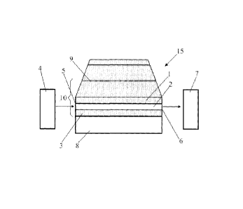
Figures 1a to lc are schematic representations of optical waveguide
interferometers according to the present invention.
CA 02693423 2010-01-18
6
Figure 1d represents an example of the intensity distribution of the
propagating modes in the transverse direction in an optical waveguide
interferometer according to the present invention.
Figure 2a illustrates an example of an interferometer and sensor according
to the present invention.
Figure 2b shows an implementation of the example of figure 2a.
Figure 3 illustrates an example of an interferometer and sensor according to
the present invention
Figure 4 illustrates an example of an interferometer and sensor according to
the present invention.
Figure 5 shows a prior art two-dimensional planar waveguide.
Figures 6 and 7 illustrate a waveguide wherein the meaning of "transverse"
and "lateral" according to the present invention is explained.
Figure 8 shows two simulations of the signals detected at the output of an
interferometer of the invention.
Figure 9 shows a simulation which represents how the refractive index of
the cladding layer affects the propagation constants of the two modes
according to
the invention.
Figure 10 represents the sensitivity versus the refractive index of the
cladding layer according to the invention.
Figure 11 shows a schematic view of an experimental set-up of a sensor
according to the invention.
Figures 12a and 12b show the response of the sensor of figure 11 under
different conditions.
Description of the Preferred Embodiments of the Invention
In the context of the present invention, the following drawings must be
considered:
As illustrated in Figure 6, a "transverse mode" of a light beam of
electromagnetic radiation is a determined intensity pattern of radiation
measured
along a line formed by a plane (plane 1 or plane YOZ) perpendicular to the
propagation direction of light beam and a plane (plane 2 or plane XOY)
perpendicular to a waveguide structure and going along the propagation
direction.
In the context of the present invention, the term "vertical" is to be
considered as a
synonym of "transverse".
As illustrated in Figure 7, a "lateral mode" of a light beam of
electromagnetic
CA 02693423 2010-01-18
7
radiation is a determined intensity pattern of radiation measured along a line
formed by a plane (plane 1 or plane YOZ) perpendicular to the propagation
direction of light beam and to a plane (plane 3 or plane XOZ), also
perpendicular
to the waveguide structure, and going along the propagation direction. In the
context of the present invention, the term "horizontal" is to be considered as
a
synonym of "lateral".
The transverse and lateral modes can be classified into TE (transverse
electric) modes and TM (transverse magnetic) modes. TE modes are those which
have no electric field in the propagation direction, while TM modes are those
which
have no magnetic field in the propagation direction.
The "dispersion" of a waveguide mode is a dependence of the propagation
velocity of said mode on the parameters of the waveguide and its surrounding
layers.
"Analyte" is any solution containing a substance which is to be detected by
the interferometer and sensor of the present invention.
The implementation of the present invention can be carried out as follows:
Figure la shows a schematic representation of a single optical waveguide
10 which supports two modes of the present invention. The two modes the
waveguide 10 is capable of supporting are transverse modes (TE or TM): a
fundamental TE or TM mode and a first order TE or TM mode. Although two
lateral
modes could be chosen, in order to overcome the already mentioned
disadvantages derived from structures confining two lateral modes, a structure
confining two transverse modes is chosen and designed.
This optical waveguide 10 acts as an interferometer. The optical waveguide
10 comprises at least one layer 2 of optically transparent material deposited
in a
laminar fashion onto a substrate 8. Preferably, the waveguide 10 comprises
several layers 1 2 3 of optically transparent material deposited in a laminar
fashion
onto a substrate 8. Layer 2 is of higher refractive index than that of
adjacent layers
1 and 3. Therefore, in this case the optical waveguide 10 is an optical slab
waveguide. The waveguide can have a single layer: One layer 1 over the
substrate is enough, because, as will be explained later, an analyte deposited
over
the upper layer (which can be the only layer) also forms a layer (a covering
layer)
located above the waveguide 10. Thus, the working principle of the
interferometer
according to which light travels through a structure with areas having
different
refractive index is fulfilled, said two areas being the monolayer waveguide 10
CA 02693423 2010-01-18
8
(supported on the substrate 8) and the analyte or covering layer deposited
thereon. Preferably, a plurality of layers 1 2 3 are used in order to optimize
the
structure.
The waveguide 10 comprises confining means capable of confining light in
lateral direction. Thanks to this confining means 9, the waveguide can support
at
least one lateral mode.
It is remarked that, in an ideal situation with a perfect waveguide, wherein
confinement in transverse direction is provided, a light beam with relatively
wide
lateral distribution (about 1 mm, for example) would propagate substantially
without divergence. This means that after propagating transversally for
several
millimeters, the light beam would maintain the same width for about 1 mm. In
this
case no rib or ridge would be required. However, wide light beams make the
waveguide bulky and impractical in the sense of integration of many waveguides
in
an array on one and the same chip. In the narrow light beams (having width of
less
than about 100 pm) propagating through these waveguides, these end up being
very divergent, i.e., after transversally propagating for several millimeters,
the light
beam diverges and expands several millimeters in lateral direction. This makes
the
device impractical. In other words, in practice, a single mode operation in
lateral
direction is extremely difficult when a simple, planar structure is used.
Likewise,
the longer the waveguide is, the more difficult it is to maintain a single
mode
operation in lateral direction. For this reason, confining means such as ribs,
guides, etc. are necessary.
Single mode operation in lateral direction also facilitates the modeling of
the
interferometer when working as a sensor and makes predictable its behavior.
Non-limiting examples of confining means 9 are a rib, a ridge or a gradient.
Appropriate waveguides are therefore: rib, ridge, gradient or other waveguide
structures. Waveguide 10 therefore allows propagation of incident
electromagnetic
radiation in the direction represented by the length of the waveguide 10,
i.e., in the
direction represented by the arrow which comes out of the optical source 4.
The
waveguide 10 is preferably a rectangular waveguide, so that the modes are
laterally and transversally confined. The fact that the waveguide is
rectangular
does not mean that in the plane perpendicular to the propagation direction the
waveguide has necessarily rectangular profile. On the contrary, the waveguide
cross section may have a small step, forming a rib waveguide structure.
In a particular embodiment, waveguide 10 is a rib type waveguide. This is
CA 02693423 2010-01-18
9
illustrated in Figure la, wherein the waveguide comprises a rib 9 in the
lateral
direction (according to the scheme of Figure 5). This rib 9 implies that the
thickness of the waveguide 10 varies along said lateral direction. Figure lb
shows
another view of the same waveguide 10 having a rib 9. Reference 19 in Figure
lc
represents another type of waveguide 10. In Figure lb, the three propagation
directions are illustrated: longitudinal, X, direction (which is the direction
of light
propagation), transverse direction, Y, and lateral direction, Z.
As can be seen, the structure of the present invention is homogeneous in
relation to the direction of light propagation, while the structure disclosed
in
JP2004145246 is homogeneous or uniform in lateral direction.
Although not illustrated in Figures la-lc, the structure also comprises a
sensor plate or area which is formed over a surface of the waveguide using a
standard photolithography and wet etching. This sensor plate is illustrated in
Figures 2 to 4.
One of the advantages of this 2D structure is that the waveguide confines
single mode light (thus is able to propagate light) for several centimeters
without
light divergence in lateral direction. Single mode operation in lateral
direction is
required because of the following reasons: First, when the waveguide is used
as
an interferometer or as a sensor, it helps to avoid ambiguities in the control
of the
interference pattern created at the waveguide end. Second, narrow waveguides,
which can only be implemented by two-dimensional structures (i.e. ribs,
ridges,
etc.) allow sequencing the sensor area to a fraction of square millimeter. The
sensor area can vary from about 0.05 to about 1 mm2. As a matter of example, a
15 mm long and 0.01 mm wide waveguide has an area of 0.15 mm2.
Sensitivity is very important in the device of the present invention. The
structure needs to be long enough in order to work as a waveguide
interferometer,
because its sensitivity is proportional to the length of the sensor plate or
area or to
the length of the bimodal waveguide. Thus, the length of the structure is
preferably
in a range approximately between 0.5 and 5 cm.
Figure lc shows how the waveguide 10 formed by an installed waveguide
may be designed by installation. Reference 18 represents an area wherein
waveguide 19 is implanted. The refractive index changes in this area 18. Said
waveguide suffers a spatial change with respect to the refractive index in
transverse and lateral directions, while geometrically it keeps being a plane
slab
structure.
CA 02693423 2010-01-18
Light from a source 4 may be transmitted to the input end of the waveguide
10 so as to illuminate layer 2. Preferably, the light source 4 provides light
having a
wavelength falling within the visible or near infrared range, said range is
approximately between 400 and 1600 nm. Light source 4 is preferably a laser.
5 The
two transverse propagating modes are thus equally excited and travel
through the length of the waveguide 10, accumulating different phase delay. At
the
output end 6 of the waveguide 10, light can radiate from the end surface onto
a
screen or measuring device 7. The intensity distribution represents the
accumulated relative phase delay. Non-limiting examples of measuring devices
10 are
detectors, such as one or more photodiodes. If more than one photodetector is
used, they are arranged in an array, such as a two-dimensional photodiode
array
or a CCD camera.
The elements already described and illustrated in Figure la form a planar
optical waveguide interferometer 15.
The two transverse modes are capable of exhibiting a measurable relative
response to a change in the wavelength of incident electromagnetic radiation
or in
a localized environment. If the refractive index of layer 1 locally changes, a
different relative phase delay accumulates and the intensity distribution is
modified
accordingly. Optical waveguide transverse modes have an electric field that is
distributed among the layers 1 2 3 and in some cases through the substrate 8
of
the waveguide structure 10. The relative amount of power contained in the
layers
1 2 3 determines the "effective refractive index" of the waveguide mode. In
turn,
the effective refractive index of a mode determines the propagation speed of
that
mode and therefore the extent of phase delay that can be accumulated as the
mode travels through the waveguide 10. If the refractive index of a layer 1 2
3
changes, the field distribution also changes, thereby resulting in a change in
the
effective refractive index. If the dispersion properties of the modes are
different,
then the change in effective refractive index can be quite large. The
propagation
constants for the fundamental and the first order modes depend on the
refractive
index of the upper or covering layer. As already mentioned, when the optical
waveguide works as an interferometer, and an analyte is deposited over the
upper
layer 1, the analyte works as a covering layer. In other words, it is
necessary that
the dispersion (i.e., the dependence of the propagation constants on the
refractive
index) is different for each mode. The interference pattern of both modes at
the
end of the waveguide is dependent on the refractive index of the combined
layers,
CA 02693423 2010-01-18
11
and therefore on the analyte solution refractive index.
Figure 1d represents an example of the intensity distribution of the
propagating modes in the transverse direction. The distance in transverse
direction is indicated in X axis in nm. The normalized intensity of the
electric field is
indicated in the Y axis (the magnitude not being so important as the response
or
shape). In Figure 1d, reference 11 represents a distribution of intensity of
the
fundamental mode. References 12 and 13 represent the distribution of intensity
of
the first order mode. As can be seen in Figure 1d, the dispersion effect is
due to
the markedly different power distribution of both modes.
The optical waveguide structure 10 forming an optical interferometer may
be advantageously manufactured using any suitable combination of conventional
materials. Examples of conventional manufacture methods are those based on
Chemical Vapor Deposition (CVD), such as Plasma Enhancement Chemical
Vapor Deposition (PECVD) or Low Pressure Chemical Vapor Deposition (LPCVD).
Chemical Vapor Deposition (CVD) is a chemical process used to produce
high-purity, high-performance solid materials, such as thin films. In a
typical CVD
process, the wafer (substrate) is exposed to one or more volatile precursors,
which
react and/or decompose on the substrate surface to produce the desired
deposit.
Microfabrication processes widely use CVD to deposit materials in various
forms,
including: monocrystalline, polycrystalline, amorphous and epitaxial forms.
These
materials include: silicon, carbon fiber, filaments, carbon nanotubes, Si02,
silicon-
germanium, tungsten, silicon carbide, silicon nitride, silicon oxynitride,
titanium
nitride, and various high-k dielectrics.
For example, the refractive index of a silicon oxynitride optical waveguide of
constant thickness (typically in a range between 0.3 and 0.5 microns) could be
selected at any level in the range between 1.457 and 2.00.
Preferably, the first and second waveguide mode can exhibit a measurable
relative response to a change in a localized environment caused by the
introduction of changes in a determined physical, biological and/or chemical
stimulus. This response is caused by the evanescent field of the modes as they
extend into the localized environment. An example of introduction of a change
in a
stimulus is a change in the refractive index of the material (e.g., analyte)
placed in
that environment. As a consequence of that change, the first and second
waveguide modes accumulate different relative phase delay, thereby causing a
measurable relative response.
CA 02693423 2010-01-18
12
This means that the planar optical waveguide interferometer 15 can
advantageously be used to detect the presence of changes in a physical,
biological and/or chemical stimulus of an analyte introduced into the
localized
environment. The optical waveguide interferometer thus becomes a chemical
sensor waveguide interferometer or a sensor based on optical waveguide. Non-
limiting examples of interaction of the stimulus with the waveguide modes are:
binding interaction, absorbance interaction or any other interaction. For
example, a
gaseous or liquid phase analyte comprising a chemical stimulus may be
introduced into the localized environment of the optical waveguide
interferometer.
Alternatively, a chemical reaction may take place in said environment, causing
changes in the nature of the chemical stimulus in situ, thereby causing a
change in
said environment.
The localized environment, also called sensor layer or plate, is preferably
an area or surface of the upper layer 1 of the optical waveguide 10 (not
illustrated
in Figures la-ic). This sensor layer may comprise absorbent or bioactive
materials. Non-limiting examples of absorbent materials are polymer materials,
such as polysiloxane or imprinted polymers. An absorbent material can absorb
gases, liquids or vapors comprising a specific chemical stimulus. Non-limiting
examples of bioactive materials are those comprising monoclonal and polyclonal
antibodies, enzymes, DNA fragments, RNA, aptamers, PNAs, functional proteins
or whole cells. A bioactive material may be appropriate for being detected in
liquid
or gas phase.
An interference pattern is generated inside the bimodal waveguide 10
(acting as an interferometer) when electromagnetic radiation propagates along
the
waveguide 10. The already mentioned changes in a stimulus located in a
localized
environment or sensor plate, or a change in wavelength, can be calculated from
the relative phase shift of the interference pattern. The measurable response
to
said change is represented by a displacement of the fringes in the
interference
pattern. The relative phase shift of the radiation within the interferometer
can be
calculated by measuring said displacement in the fringes. At the output 6 of
the
waveguide 10, the electromagnetic radiation is coupled into free space. The
interference pattern can thus be recorded in a conventional manner (for
example,
using a single detector 7 which measures the changes in the radiation
intensity or
using a plurality of such detectors 7 which monitor the changes occurring in a
number of fringes or in the entire interference pattern). Such detectors 7 are
CA 02693423 2010-01-18
13
preferably one or more photodetectors and upon using more than one
photodetector, they are arranged in an array, as a two-dimensional photodiode
array.
As shown in Figure la, light from the source 4 is focused in the input end 5
of the waveguide 10 and propagated in the form of electromagnetic radiation,
which can be coupled into the first and second waveguide modes in different
ways.
In a particular embodiment, radiation is simply coupled to the waveguide 10
by means of the end of a face 5 of said waveguide 10. This is also called "end
fire
type procedure". In this case, the light source (e.g., laser) is integrated
with the
laminate structure 1 2 3 on the common substrate 8. Non-limiting examples of
substrates 8 are indium phosphate and silicon substrates.
Alternatively, the interferometer 15 comprises other coupling means for
coupling the incident electromagnetic radiation into the first (fundamental)
and
second (first-order) waveguide modes of the waveguide 10. This coupling of
both
modes is done substantially simultaneously. Non-limiting examples of coupling
means, apart from end-fire, are direct focusing (for example, by means of a
HeNe
laser), prism coupling, diffraction grating coupling or mirror coupling.
Optionally, the incident light or electromagnetic radiation may be oriented
(e.g., linearly polarized) as desired using appropriate polarizing means. Non-
limiting examples of polarizing means are polarizing cube beam splitters,
linear
polarizers and wire-grid polarizers.
Optionally, the incident light or electromagnetic radiation may be focused
using focusing means. Non-limiting examples of such means are: a lens, a
microlens and an optical system comprising a series of lenses.
Optionally, the output electromagnetic radiation pattern may be projected
towards the aforementioned detector by means of projecting means. Non-limiting
examples of projecting means are objective lenses, lenses and direct
projection
onto multisection photodetector.
Next, some examples of interferometers based on bimodal waveguides and
sensors based on interferometers are described.
Figure 2 shows an example of interferometer 25 which comprises a bimodal
waveguide 20, formed by one or more layers as illustrated in Figures la, lb
and
1 c. On its upper surface, the waveguide 20 comprises a sensor plate 21,
wherein
an analyte can be deposited. Waveguide modes (the fundamental and the first
CA 02693423 2010-01-18
14
order ones) are excited in the waveguide 20 using direct focusing of light
from a
laser source (not shown in Figure 2) by means of an objective lens 22. A
structure
is considered non-symmetrical in transverse direction if the distribution of
the
refractive index across the structure in transverse direction is not
symmetrical with
respect to the symmetry axis of the structure. The symmetry axis of the
structure is
an axis going in the direction of light propagation and crossing the plane
perpendicular to the light propagation direction in a point where maximum
intensity
of electromagnetic field distribution of a transverse fundamental mode is
located.
The structure of Figure 5 is thus non-symmetrical. Because the structure is
not
symmetrical the central axis of the objective lens can be misaligned in the
transverse direction with respect to the symmetry axis of the waveguide layer,
both
the zero (fundamental) and the first order modes are excited. The two
transverse
modes propagate with different velocities and pass by the sensor plate 21. The
interference pattern formed at the output end 16 of the waveguide 20 is
projected
on a two-section photodetector (TSP) 27 using an objective lens 29 as a
projecting
and magnifying means. The position of the maximum of the interference pattern
is
defined, among other parameters, such as the refractive index, the thickness
of
each layer, the length of the waveguide and the width of the waveguide, by the
initial phase of the excited waves and by the refractive index of the analyte
passing through the sensor plate 21. It is thus registered the change in the
refractive index of the covering layer (measured in the sensor plate) caused
by a
chemical or biological reaction which has occurred on the waveguide surface or
by
changes in the analyte solution.
Blocks 28 refer to the walls of a microfluidic cell which can be attached to
the waveguide 20 in order to provide flow and exchange of the analyte. They
are
not part of the present invention.
Figure 2b shows an implementation of the example of Figure 2a. The
interference pattern in the transverse direction can be distributed with the
maximum located in the lower or in the upper part of the waveguide, as shown
in
Figure 2b, where the distributions of light intensities in the waveguide cross
section are shown in the inset. The distributions are designed for a waveguide
with
refractive index of 2.0 (silicon nitride) and with thickness of 400 nm. The
phase
difference between the modes varies by -rr radian from one curve to the other.
Under certain conditions the difference between the energies concentrated in
the
top and in the bottom sections of the photodetector can reach -17 dB. The
output
CA 02693423 2010-01-18
intensity is proportional to the amount of light coupled to the waveguide at
the
input. If absorption over the waveguide is constant, then the total light
power at the
exit is proportional to the power coupled at the input except for some changes
due
to reflectivity from the output facet, which according to simulations is
slightly
5 changing with the interference pattern movement. Assuming that the
function of
the reflectivity change is known, the ambiguities due to coupling efficiency
variations can be reduced, because monitoring with a two-section photodetector
(TSP) allows registering simultaneously both the total power and the shift in
the
distribution of light exciting the bimodal waveguide (BiMW).
10 Figure 3 illustrates an example of interferometer 35 which comprises a
bimodal waveguide 30, formed by one or more layers as illustrated in Figures
la,
lb and lc. On its upper surface, the bimodal waveguide 30 comprises a sensor
plate 31 wherein an analyte can be deposited. The interferometer 35 comprises,
at
both ends of said waveguide 30, single mode waveguides 31 32. Both input
15 waveguide 31 and output waveguide 32 are single mode in transverse and
lateral
directions. The only parameter which varies from the single mode part 31 32 to
the
bimodal part 30 is the thickness. This implies that the thickness of these two
waveguides 31 32 is less than the thickness of the bimodal waveguide 30. Light
is
coupled into the input waveguide 32 by any conventional coupling means, such
as
end-fire, direct focusing, prism coupling or diffraction grating coupling. The
particular coupling means used in the interferometer 35 of Figure 3 is direct
coupling by means of a focused lens 34. Because the structure is not
symmetrical
at the junction input waveguide 32 - bimodal waveguide 30, the fundamental
mode
(which is the only mode which propagates through the input waveguide 32)
splits
into two modes: the fundamental and the first order ones, in the bimodal
waveguide 30. The ratio between the modes amplitudes is defined by the
geometry of the structure or, more precisely, by the thickness of the
waveguides
32 30 31. Optimization of the wavelength thickness is an engineering problem
which can be solved on the basis of conventional modeling methods. The amount
of light coupled into the output waveguide 33 depends on the intensity
distribution
at the junction bimodal waveguide 30 - output waveguide 33. In this example,
the
reading of the output signal coming out of the output waveguide 33 is
performed
by a conventional photodetector 37, such as a photodiode. The output
interference
pattern is projected on said photodetector 37 using an objective lens 39 as a
projecting means.
CA 02693423 2010-01-18
16
Figure 4 illustrates an example of interferometer 45 which comprises a
bimodal waveguide 40 deposited on a substrate 48. On its upper surface, the
bimodal waveguide 40 comprises a sensor plate 41 wherein an analyte can be
deposited. Light is coupled into the bimodal waveguide 40 by means of a
diffraction grating coupler 42 mounted or integrated on the bimodal waveguide
40.
The fundamental and the first order modes are excited by light beams (e.g.,
laser)
coming from a single source (not illustrated in Figure 4) and directed to the
diffraction grating coupler 42 at different incidence angles 00 B1
corresponding to
the phase match condition for each mode. Both modes are diffracted by
diffraction
grating coupler 42 and propagate through the bimodal waveguide.
As already mentioned, sensitivity is directly proportional to the length of
the
sensor plate or to the length of the bimodal waveguide. Next, an analysis of
the
sensitivity of the device of Figure 2b is done.
If the transfer matrix approach is used, the distributions of light
intensities
are created for each mode of a waveguide with a refractive index 2.0 (silicon
nitride) on a silica substrate (refractive index 1.46) and a variable
refractive index
of the cladding layer. Then, the distributions of the interference pattern at
the
waveguide exit and the corresponding signals generated by the photodetector
sections are calculated as a function of the phase shift between the modes.
The
signals produced by the photodetector sections are recalculated into a
relative
change, Sr, of the output signal according to the expression:
U
=
( 1 )
U +
Uup, Udown are the signals generated by the upper and the lower sections of
the
photodetector respectively. The results of the simulations (Sr versus the
phase
shift) are presented in Figure 8. All calculations were performed for a
wavelength
of 632.8 nm. The amplitudes of the modes were previously normalized to unity.
The curve built for the 400 nm thick waveguide (solid line) is a little
steeper than
that for 300 nm thick waveguide (dash line). The reason is that the non-
symmetrical distribution of the waveguide modes which is getting stronger for
the
thin waveguides. However, the difference between the curves slopes is not that
remarkable: 4/-rr for the waveguide with thickness of 300 nm and 4.3/-rr for
the 400
nm thick waveguide.
Considering a uniform bimodal waveguide with the modes propagating until
reaching a distance L and the exit of the waveguide, the sensitivity of the
device,
CA 02693423 2010-01-18
17
i.e., the relationship between the change occurred in the output signal and
the
change occurred in the refractive index of the cladding layer, is expressed by
the
formula:
dSr dSr aco
Sens = ¨ (2)
d
nd indicates the refractive index of the cladding layer, and cp is the phase
difference of both modes.
The phase difference due to a change in the refractive index of the cladding
layer after a distance L is expressed as:
= =( ¨ ,i4j= ). L (3)
An
L is the length of the sensor plate, A is the wavelength, An'?ff , if is
the change of
the effective refractive index of the zero and the first order modes
respectively due
to the changes in the refractive index of the cladding layer. After
substitution of (3)
with (2) the expression for the sensitivity of the device is obtained:
)Sr an,'ff an,?ff 2rt
Sens = wcT) and ond 7-1 L (4)
The refractive index of the cladding layer differently affects the propagation
0
constants no' of the fundamental and neff of the first order modes. The
derivatives
aneiff an:)õ
atia , an, are presented in Figure 9 as a function of the refractive index of
the
cladding layer. Dash lines correspond to the fundamental mode, solid lines
correspond to the first mode. The waveguide thickness corresponds to: o - 300
nm, a - 350 nm, A - 420 nm, V - 470 nm. Obviously, the deeper the waveguide
modes penetrate into the cladding, the more effective refractive index
modulation
for both modes. The penetration of the modes is inversely proportional to the
waveguide thickness and directly proportional to nd. The derivatives shown in
Figure 9 referred to both modes, increase as the refractive index of the
cladding
layer increases. However, the propagation constant of the first order mode is
strongly affected by the cladding refractive index changes. The difference
between
= CA 02693423 2010-01-18
18
the derivatives is especially significant, and subsequently the sensitivity is
higher,
in thin waveguides. For example, in a 300 nm thick waveguide, sensitivity can
be
three times higher than in a 470 nm thick waveguide.
The sensitivity expressed in terms of phase shift per unit of refractive index
can be seen in Figure 9 and expression (3). Thus, on a 300 nm thick and 10 mm
long waveguide, a phase change of 2 TT can be reached, if the refractive index
of
the cladding layer changes by 6x10⁻⁴ RIU (Refractive Index Unit), when nc, is
around 1.34.
In Figure 10 the sensitivity Sens calculated by means of expression (4) is
plotted versus the refractive index of the cladding layer for four different
waveguide
thicknesses: o - 300 nm, a - 350 nm, A - 420 nm, V - 470 nm. The sensitivity
is the
change in the output signal per unit refractive index change in the cladding
layer.
The calculations were performed assuming a 10 mm long waveguide. This
parameter defines the noise floor which is allowed in the detection circuitry
in order
to distinguish the changes in the interference pattern. It can be observed
that an
accuracy of 1% is enough for the reading of the output signal when working
with
waveguides thinner than 400 nm. The sensitivity of the proposed device is
comparable to the sensitivity of integrated MZI fabricated by silicon
technologies.
The following is an example of preparation: A silicon wafer polished at one
side is subjected to high temperature oxidation. A layer of silicon dioxide of
about
2 pm thick is formed on both sides of the wafer (the side where components are
placed, forming the waveguide, and the back side), as a result of this
process. A
layer of silicon nitride of about 400 nm thick is deposited by LPCVD technique
on
both the components and the back sides. A layer of PECVD silicon dioxide is
deposited on the front side of the wafer. Waveguides are patterned on the
front
side using conventional photolithography and wet etching in buffered Hydro
Fluoridric (HF) acid. Photoresist is removed with oxygen plasma. The wafer is
immersed in HF solution for a time sufficient to remove the silicon dioxide
mask
and to form simultaneously ribs over the silicon nitride. Selective etching is
used
(the thickness of PECVD oxide is chosen proportional to the rib height). The
selectivity of the etching (silicon nitride) is approximately 1000/14 if the
etching is
done with a SiO-etch solution (similar to HF10 /0). This technology allows
manufacturing rib waveguides with a height of about 4 nm and width of about 4
pm. The resulting waveguide can support two transverse modes. It is therefore
bimodal, having a fundamental mode and a first order mode. A layer of silicon
CA 02693423 2010-01-18
19
oxide is then deposited on the part of the components as a protection layer. A
sensor plate is formed on the surface of the waveguide by means of standard
photolithography and wet etching in SiO-etch solution.
For the current experiment a 3 pm wide waveguide which supported a
single mode in lateral direction was used. The wafer was diced in chips and
the
chips were polished to get the end faces of the waveguides polished. The chip
was mounted on an aluminium base and covered with a polymethylmetacrylate
(PMMA) microfluidic header which had a channel in order to provide the reagent
flow over the waveguide. The length of the sensor plate L was 3 mm.
Next a biosensor based on a bimodal optical waveguide according to the
invention is described. Experiments on the detection of the reagent refractive
index changes were done by injecting water:glycerine solution into the
channel.
The schematic view of the experimental set-up is presented in Figure 11. The
flow
was provided by a peristaltic pump. Light was launched into the waveguide 20'
through an objective lens 52 focused to a beam from a He-Ne laser 4'. In this
case, the laser is a HeNe Laser of 10 mW, which also comprises a beam
expander. Slight misalignment of the objective with respect to the waveguide
in
vertical direction allows for excitation of both modes simultaneously. Light
was
collected by another objective lens 29' and the image of the waveguide facet
was
projected onto the TSP 27'. The signal was stabilized while deionized water
was
passing by the sensor plate 51. Valve 53 is used for directing the flow with
or
without reagent to a channel passing in the microfluidic cell by the sensor
plate 51.
Then solutions with three different concentrations, with indexes of refraction
1.3356, 1.337, and 1.39, were injected into the channel. In Figures 12a and
12b
the time diagrams of the output signal are presented. The experiments were
carried out on different samples and at different times, so the modulation
amplitudes and sensitivities vary from one experiment to another. Injection of
highly concentrated solution of glycerine (44 % vol. and refractive index of
1.39)
caused a strong phase change and 18 Tr oscillations (see Figure 12a).
Injection of
low concentrated solution of glycerine (2.2% or 3.3% vol. with corresponding
refractive indexes of 1.3356 and 1.337, correspondingly) resulted in a weak
phase
changes and almost Tr and 2 Tr oscillations, respectively (see Figure 12b).
Analyzing the results of the experiments and assuming the refractive index
of deionized water of 1.333, a phase change of about 2 7 per 0.006 cladding
R1U
change was observed. The curve slope at the most sensitive position is around
CA 02693423 2010-01-18
0.06 per 10-4 RIU. Subsequently in order to detect index variation of 10-6 RIU
an
accuracy of 6x10⁻⁴ (0.06%) in measuring the absolute value of the output
signal is
required. Stability of the output signal must be of the same order of
magnitude.
Assuming the sensor plate to be 10 mm long, the sensitivity is 0.002 per 10-6
RIU
5 change. Although there are some discrepancies between the theoretically
predicted sensitivities and the experimentally demonstrated ones, they are due
to
the coupling technique used in the experiment, which cannot always guaranty
the
appropriate amplitude ratio between the excited modes. In other words, this
discrepancy is a consequence of engineering limitations.
10 The present invention further provides a method for detecting the
introduction of changes (e.g., the amount or concentration of a stimulus) in a
determined chemical, biological or physical stimulus in a localized
environment.
The method comprises the following steps carried out in a bimodal optical
waveguide interferometer like the one shown in Figures la, lb and lc:
15 (a) defining a sensor plate 21 31 41 in a localized environment of the
upper
part of the waveguide 10 20 30 40;
(b) placing a chemical, biological or physical stimulus or analyte in said
sensor plate 21 3141;
(c) introducing or causing changes in said chemical, biological or physical
20 stimulus in said sensor plate 21 31 41;
(d) coupling a fundamental mode and a first-order mode of electromagnetic
radiation into said optical waveguide 10 20 30 40, in such a way that when
both
modes travel through the sensor plate 21 31 41 defined in the waveguide, they
suffer a variation in its characteristics, such as a phase delay, which is
dependent
on the changes in said chemical, biological or physical stimulus;
(e) at the output of said waveguide, measuring the response of said
fundamental mode relative to the response of said first-order mode; and
(0 relating said relative response of both modes to the changes in the
chemical, biological or physical stimulus.
Preferably, step (e) comprises:
(el) generating a pattern of interference fringes; and
(e2) measuring a displacement in the interference pattern.
Preferably, step (0 comprises:
(f1) relating the displacement in the interference pattern with the presence
of changes in the determined chemical, biological or physical stimulus.
CA 02693423 2010-01-18
=
21
In conclusion, an interferometer and a biosensor based on a bimodal optical
waveguide having a simple design are presented.
In this text, the term "comprises" and its derivations (such as "comprising",
etc.) should not be understood in an excluding sense, i.e., these terms should
not
be interpreted as excluding the possibility that what is described and defined
may
include further elements, steps, etc.
In the context of the present invention, the terms "around", "about",
"approximately" and "substantially" and terms of the same family (such as
"approximate", etc.) should be understood as indicating values very near to
those
which accompany the aforementioned term. That is to say, a deviation within
reasonable limits from an exact value should be accepted, because the expert
in
the technique will understand that such a deviation from the values indicated
is
inevitable due to measurement inaccuracies, etc.
On the other hand, the invention is obviously not limited to the specific
embodiment(s) described herein, but also encompasses any variations that may
be considered by any person skilled in the art (for example, as regards the
choice
of materials, dimensions, components, configuration, etc.), within the general
scope of the invention as defined in the appended claims.