Note: Descriptions are shown in the official language in which they were submitted.
CA 02693626 2010-01-08
WO 2009/007500 PCT/F12008/050379
1
METHOD AND DEVICE FOR CAPACITIVE DETECTION OF
OBJECTS
The present invention relates to capacitive detection of objects, e.g.
human beings.
BACKGROUND
Presence of bodies or objects may be detected by determining a
change of capacitance between two plates. The presence of an object
causes a change in the dielectric constant between the plates, which in
turn causes a change in the capacitance formed by said two plates,
when compared with a situation where the object is far away from said
plates.
A capacitive sensor may be used e.g. to detect movements of people
e.g. in an anti-theft alarm system.
The absolute value of the capacitance of a capacitive sensor is
typically very small. Electro-magnetic noise coupled into the sensor
and to a monitoring circuit makes it difficult to detect small changes in
said capacitance.
It is known that the capacitance value of a capacitor may be measured
by coupling said capacitor as a part of an RC-circuit, and by
determining the time constant of said RC-circuit. The resistor and the
capacitor are connected in series, and the capacitor is charged through
the resistor, starting from a defined voltage. The charging time can be
characterized with the time constant. The time constant of the circuit,
formed by the capacitor and the resistor, is determined either by
measuring the time until a predetermined voltage level is reached or by
measuring the voltage after a predetermined loading time. When the
time constant and the resistance are known, the capacitance can be
calculated.
CA 02693626 2010-01-08
WO 2009/007500 PCT/F12008/050379
2
This method can be used in measuring the capacitance of a capacitive
sensor. A problem of the method is that the energy of a measured
signal is very low, if the measured capacitance is low. Therefore, it is
difficult to attain sufficient precision by measuring the charging time or
the voltage attained after a predetermined loading time. Furthermore,
electromagnetic radiation can easily interfere with the measurement. In
practice, the capacitance of the sensor is so low that the charging time
is also short and cannot be measured accurately enough e.g. by using
a low-cost micro controller. Furthermore, a measurement based on this
principle does not contain any kind of low-pass filter, which allows
aliased high-frequency noise to appear on top of the signal to be
measured.
It is known that the capacitance value of a capacitor may be measured
by coupling an alternating voltage to said capacitor, and by determining
the impedance of said capacitor.
The capacitor resists alternating current flow due to its impedance. The
impedance is inversely proportional to the capacitance in a frequency
domain. The impedance of the unknown capacitor can be compared
with the impedance of a known capacitor by using, for example, a
bridge comparison circuit, such as the Wheatstone bridge. This method
requires complicated circuits and is therefore expensive.
It is known that changes in the capacitance value of a capacitor may be
detected by coupling said capacitor as a part of a tuned oscillation
circuit.
A capacitive sensor arrangement may comprise a resonance circuit
composed of an unknown sensor capacitor and a known coil
(inductance). When the capacitance of the sensor capacitor reaches a
defined value, the circuit starts to resonate and the amplitude of the
oscillation increases suddenly. It can be easily measured whether the
circuit is resonating or not. This method is extremely sensitive, but only
in a certain narrow capacitance range. When a wider range is required,
this method is not practicable.
CA 02693626 2010-01-08
WO 2009/007500 PCT/F12008/050379
3
SUMMARY
The object of the invention is to provide a device and a method suitable
for capacitive detection of objects.
The presence of an object changes the capacitance of a capacitive
sensor, i.e. a sensor capacitor, when compared with a situation when
the object is far away. Movement of an object in the vicinity of the
capacitive sensor changes the capacitance of the sensor capacitor.
According to a first aspect of the invention, there is provided a device
for capacitively detecting an object, said device comprising:
- a capacitive sensor having a sensor capacitor formed between at
least one first capacitive element and at least one second capacitive
element such that the presence of said object can change the
capacitance of said sensor capacitor,
- a voltage supply,
- a first switch to couple said sensor capacitor to said voltage supply in
order to charge said sensor capacitor,
- a tank capacitor,
- a second switch to couple said sensor capacitor to said tank capacitor
in order to transfer charge from said sensor capacitor to said tank
capacitor and to change the voltage of said tank capacitor,
- at least one switch driver unit to control said charging and charge
transfer by opening and closing said switches several times such that
said switches are not in the closed state simultaneously,
- a voltage monitoring unit to monitor the voltage of said tank capacitor,
and
- a controller to determine at least one measurement value which
depends on the rate of change of the voltage of said tank capacitor.
According to a second aspect of the invention, there is provided a
method for capacitively detecting an object by using a capacitive
sensor having a sensor capacitor formed between at least one first
CA 02693626 2010-01-08
WO 2009/007500 PCT/F12008/050379
4
capacitive element and at least one second capacitive element such
that the presence of said object can change the capacitance value of
said sensor capacitor, said method comprising:
- charging said sensor capacitor by coupling it to a voltage supply,
wherein said voltage supply is disconnected from a tank capacitor
during said charging,
- transferring charge from said sensor capacitor to a tank capacitor,
wherein said voltage supply is disconnected from said tank capacitor
during said charge transfer,
- repeating said charging and charge transferring several times,
- monitoring the voltage of said tank capacitor, and
- determining at least one measurement value which depends on the
rate of change of the voltage of said tank capacitor.
The unknown capacitance of the sensor capacitor is determined by a
measuring circuit according to the invention. According to the invention,
a known tank capacitor is charged by transferring charge several times
from a voltage supply to said tank capacitor by using the sensor
capacitor. Charging increases the voltage of said tank capacitor at a
rate which is proportional to the capacitance of the sensor capacitor.
Movement of the object may be detected by comparing a first rate of
change with a second rate of change, which was measured earlier. If
the rate of change of the voltage of the tank capacitor is increased, it
may be determined that an object has moved closer to the capacitive
sensor. A change in the rate of change (second derivative) of said
voltage indicates that an object has moved in the vicinity of the
capacitive sensor.
The voltage of the sensor capacitor represents a low-energy signal,
and the voltage of the tank capacitor represents a high-energy signal.
Transferring charge to a larger known capacitor by the smaller sensor
capacitor makes it possible to integrate the low energy signal into the
high energy signal before e.g. analog-to-digital conversion.
Consequently, the sensitivity of the measuring device to
electromagnetic interferences is considerably reduced.
CA 02693626 2010-01-08
WO 2009/007500 PCT/F12008/050379
Operating parameters of the measuring device may also be optimized
so as to optimize resolution, measurement range, and/or data
acquisition rate. Said operating parameters may also be adjusted by
software.
5
The measuring device inherently comprises a low pass filter, which is
formed from the smaller sensor capacitor, a charge-transferring switch
and the larger tank capacitor. Said low-pass filter effectively attenuates
noise cause by high frequency interference.
It is known that small capacitances may be measured accurately by
using dangerously high voltages, e.g. in the order of 100 V or higher.
Thanks to the invention, changes in the capacitance may be accurately
monitored by using lower voltages, e.g. 24 V or less.
The embodiments of the invention and their benefits will become more
apparent to a person skilled in the art through the description and
examples given herein below, and also through the appended claims.
BRIEF DESCRIPTION OF THE DRAWINGS
In the following examples, the embodiments of the invention will be
described in more detail with reference to the appended drawings, in
which
Fig. 1 shows, in a three-dimensional view, a capacitive proximity
sensor,
Fig. 2 shows a schematic diagram of the switched capacitor
measurement circuit according to the invention,
Fig. 3 shows the circuit diagram of a capacitance measuring
device comprising a voltage comparator,
Fig. 4 shows a timing chart for the device of Fig. 3,
CA 02693626 2010-01-08
WO 2009/007500 PCT/F12008/050379
6
Fig. 5 shows the circuit diagram of a capacitance measuring
device comprising an analog switching unit DG403DJ,
Fig. 6 shows, by way of example, an output of a measurement,
Fig. 7a shows, by way of example, possible choices of
measurement parameters,
Fig. 7b shows the cut-off frequency for capacitance switching,
Fig. 8 shows the circuit diagram of a capacitance measuring
device comprising an analog-to-digital converter,
Fig. 9 shows, by way of example, a timing chart for the device of
Fig. 8,
Fig. 10a shows, by way of example, temporal evolution of the
capacitor voltage for the device of Fig. 3,
Fig. 10b shows, by way of example, temporal evolution of the
capacitor voltage for the device of Fig. 8
Fig. 11 shows, in a three-dimensional view, a capacitive sensor
array,
Fig. 12a shows, in a top view, a sensor web
Fig. 12b shows a cross-sectional view of the web of Fig. 12a,
Fig. 13 shows the circuit diagram of a differential capacitance
measuring device,
Fig. 14a shows, in a three-dimensional view, a capacitive proximity
sensor comprising three plates, and
CA 02693626 2010-01-08
WO 2009/007500 PCT/F12008/050379
7
Fig. 14b shows, in a three-dimensional view, a capacitive proximity
sensor comprising two plates, said sensor being disposed
over an electric ground.
All drawings are schematic.
DETAILED DESCRIPTION
Referring to Fig. 1, a capacitive sensor 20 may comprise a first
conductive element 10a, and a second conductive element 10b. The
elements 10a, 10b are electrically insulated from each other. The
elements 10a, 10b may have any form. One or both elements 10a, 10b
may be conductive structures consisting of several parts. Electric
ground or earth may also be used as a conductive element 10a or 10b
(see Fig. 14b). The first element 10a has a connecting terminal TO and
the second element has a connecting terminal T1.
Advantageously, the elements 10a, 10b are plates. The plates 10a,
10b may be disposed in or on an electrically insulating substrate 5.
The plates 10a, 10b form a capacitive system together with the
medium located between said plates 10a, 10b. Said capacitive system
CX has a capacitance value CX. For simplicity, the symbol CX is herein
used to refer to the physical entity (capacitor) as well as to the
measurable quantity (capacitance).
The presence of an object BOD1 in the vicinity of the sensor 20
changes the dielectric permittivity of the medium between the plates
10a, 10b. Thus, the presence of the object BOD1 changes the
capacitance CX, when compared with a situation when the object
BOD1 is far away from the sensor 20.
The capacitance CX depends on the distance between the object
BOD1 and the sensor 20, as well as on the material, size and form of
CA 02693626 2010-01-08
WO 2009/007500 PCT/F12008/050379
8
the object BOD1. Thus, said capacitive system CX represents an
unknown capacitor.
The capacitance CX may be e.g. smaller than or equal to 5 nF when
the object BOD1 is far away from the sensor 20, or even smaller than
or equal to 1 nF in order to improve spatial resolution. A small area of
the plates 10a, 10b may be needed to ensure sufficient spatial
resolution.
The dielectric permittivity of the object typically deviates from the
dielectric permittivity of air. Typically, the presence of the object BOD1
increases the capacitance CX. Also the presence of a conductive
object BOD1 increases the capacitance CX. This is because an
electrically conductive object can be understood to have a substantially
infinite dielectric permittivity.
The sensor 20 may comprise an electrically insulating layer (see e.g.
Fig. 12b to prevent electric contact between the plates 10a, 10b and
the object BOD1.
For an optimum spatial resolution and signal-to-noise ratio, the size of
the plates 10a, 10b may be in the same order of magnitude as the size
of the object BOD1 to be detected. If the object BOD1 is e.g. the foot of
a person, the dimensions of the plate 10a may be e.g. in the range of 3
to 30 cm in the directions DX and DY.
DX, DY and DZ are orthogonal directions. The substrate 5 may be in a
plane defined by the directions DX and DY.
Referring to Fig. 2, a switched capacitor circuit is a circuit, which
comprises a capacitor connected between two switches so that the
capacitor is alternately charged and discharged. This kind of a circuit
acts like a resistor.
Fig. 2 shows a switched capacitor circuit, which comprises the
unknown sensor capacitance CX, a first switch S1, a second switch S2,
CA 02693626 2010-01-08
WO 2009/007500 PCT/F12008/050379
9
and a voltage supply 40. The voltage supply provides a voltage V1.
The switches S1 and S2 are opened and closed at a switching
frequency fsW in such a way that the switches S1, S2 are not in the
closed state simultaneously. For example, the first switch may be in the
closed (conducting) state when the second switch S2 is in the open
(non-conducting) state, and vice versa.
A voltage supply 40 provides a voltage V1. Closing of the switch S1
transfers charge to the sensor capacitor CX. Opening of the switch S1
and closing the switch S2 transfers the charge from the sensor
capacitor CX to the tank capacitor C2. Opening and closing of the
switches S1, S2 alternately several times increases the voltage of the
tank capacitor C2 in a stepwise manner. The switching may be
continued e.g. until a predetermined voltage over the tank capacitor C2
is attained.
Fig. 3 shows a proximity detecting device 100, which may comprise a
capacitive proximity sensor 20, switches S1, S2, S3, a tank capacitor
C2, a voltage supply 40, a reference voltage source 58, a comparator
50, and a controller 60. The voltage supply 40 provides a voltage V1.
The capacitive sensor 20 is represented by the sensor capacitor CX.
The first node of the voltage source 40 is coupled to the first terminal
TO of the sensor capacitor CX. The second node of the voltage source
40 is coupled to the second terminal T1 of the sensor capacitor CX by
the switch S1. Thus, the sensor capacitor CX may be charged to the
voltage V1 of the supply 40.
The terminal TO may also be connected to the ground GND, e.g. to the
earth. However, this is not always necessary.
First, the tank capacitor C2 may be discharged by closing the switch
S3. The switch S3 is subsequently opened and kept in the open state.
The sensor capacitor CX is now charged by closing the switch S1,
while the switch S2 is in the open state. Then, the switch S1 is opened
CA 02693626 2010-01-08
WO 2009/007500 PCT/F12008/050379
and charge is transferred from the sensor capacitor CX to the tank
capacitor C2 by closing the switch S2. The transferred change
increases the voltage VX over the tank capacitor by a small amount.
5 The capacitance of the tank capacitor C2 may be e.g. greater than or
equal to 10 times the minimum capacitance value of the sensor
capacitor CX, preferably greater than or equal to 100 times the
capacitance value of said sensor capacitor CX.
10 The voltage VX of the tank capacitor is increased by closing and
opening the switches S1 and S2 consecutively several times until the
voltage VX reaches or exceeds the reference voltage Vref provided by
the reference voltage source 58.
The voltages VX and Vref may be coupled to inputs 51, 52 of a
comparator 50. The output 53 of the comparator 50 may be coupled to
an input 61 of the controller 60.
The controller 60 may be arranged to discharge the tank capacitor C2
by closing the switch S3 when the state of the comparator output 53 is
changed.
The controller 60 may be arranged to discharge the tank capacitor C2
by closing the switch S3 after a predetermined time from the change of
state of the comparator output 53.
The switches S1, S2, S3 may be controlled by at least one switch
driving unit 90, which may be a separate component or incorporated in
the controller 60.
The controller 60 may be arranged to count the number Nk of charge
transfer cycles, i.e. closing times of the switch S2 needed to change
the state of the comparator output. The controller 60 may be arranged
to send the number Nk to an external data processing device 200 via
terminals 62, 201.
CA 02693626 2010-01-08
WO 2009/007500 PCT/F12008/050379
11
The number Nk, or further information dependent on said counted
number Nk, represents a measurement result.
Said further information may be e.g. a time constant, a time period Tk
needed for the tank capacitor voltage CX to reach a predetermined
voltage, a voltage VX of the tank capacitor C2 attained after a
predetermined time period TFIX, the absolute value of the sensor
capacitor CX, a change of the capacitance of the sensor capacitor CX
when compared with its previous value, or a relative change (e.g. +1 %)
of the capacitance of the sensor capacitor CX when compared with its
previous measured value.
Data acquisition rate of the proximity detecting device 100 means the
number of independent capacitance values CX measured per unit time.
Switching frequency means the number of closing cycles of the second
switch S2 per unit time. The switching frequency may be by several
orders of magnitude higher than the data acquisition rate.
The reference voltage Vref may be lower than or equal to 30% of the
voltage V1 of the voltage supply 40 so as to provide a substantially
linear relationship between the count number Nk and the capacitance
value CX.
The reference voltage source 58 may comprise e.g. a voltage divider
formed by resistors R1 and R2. An advantage of the voltage divider is
that the measurement result is substantially independent of the
absolute voltage V1. Also a reference voltage supply based on e.g. a
Zener diode may be used.
The data processing device 200 may be e.g. a computer of a
surveillance system.
The absolute value of the unknown sensor capacitance CX may be
determined by the device 100. The absolute value CX of the sensor
capacitance may be calculated based on the known values of tank
capacitance C2, on the known switching frequency, and on the known
CA 02693626 2010-01-08
WO 2009/007500 PCT/F12008/050379
12
ratio between the voltage VX of the tank capacitor C2 and the voltage
V1 of the voltage supply 40.
An even more accurate calculation can be made when the impedances
(resistivity and capacitance) of the switches S1 and S2 are taken into
account.
The capacitance values CX determined by calculation may be made
even more accurate by calibration, e.g. by determining a calibration
coefficient by coupling a known capacitor to the terminals TO and T1.
However, in many cases it is not needed to determine the absolute
value of the sensor capacitance CX. The device 100 may be arranged
to detect a change in the sensor capacitance CX. The change may be
determined as a relative change, e.g. 1% increase when compared
with a previous measured value.
The switching frequency and/or the capacitance C2 may be adjustable
in order to optimize data-acquisition rate, accuracy and/or resolution.
E.g. the controller 60 may be arranged to make said adjustment based
on a previous measured value. The data-acquisition rate, accuracy
and/or resolution may be adjusted by software.
The capacitance C2 may be adjusted e.g. by coupling a further
capacitor in parallel by a further switch.
Fig. 4 shows the timing chart for the device of Fig. 3. The first, the
second, the third, and the fifth curve from the top show the logical
states of the switches S1, S2, S3 and the comparator output,
respectively. The fourth curve from the top shows the temporal
evolution of the voltage VX of the tank capacitor.
The switch S3 is closed at the time t4,k_1 in order to discharge the tank
capacitor C2. The switch S3 may be kept closed for a predetermined
time in order to ensure that the tank capacitor C2 is discharged to a
sufficient degree.
CA 02693626 2010-01-08
WO 2009/007500 PCT/F12008/050379
13
t denotes time. k is an integer which indicates the index of a currently
measured result. The logical state 0 denotes an open switch and the
logical state 1 denotes a closed switch. At least one of the switches S1,
S2 should be open during discharging of the tank capacitor C2.
The switch S3 is opened at the time tl,k and the sensor capacitor CX is
charged by closing the switch S1. S2 is kept in the open state. The
switch S1 is opened at the time t2,k and the switch S2 is closed in order
to transfer charge from the sensor capacitor CX to the tank capacitor
C2. The switches S1 and S2 are opened and closed several times
alternately until the voltage VX of the tank capacitor reaches or
exceeds the reference voltage Vref.
The voltage VX of the tank capacitor becomes equal to the reference
voltage Vref at the time t3,k.
The switch S3 is closed at the time t4,k in order to discharge the tank
capacitor C2 again.
The time period Tk between the times t2,k and t3,k is proportional to the
count number Nk, i.e. the number of consecutive opening and closing
cycles of the switches S1, S2 needed to attain the reference voltage
level Vref. The length of the time period Tk, or the corresponding count
number Nk represents a measurement result.
A new charging and charge transfer sequence by using the switches
S1 and S2 is started again at the time t1 k+1 in order to determine the
next count number Nk+1 and/or the next time period Tk+1.
Fig. 5 shows an implementation of the device by using a
microcontroller IC1 and an analogue semiconductor switching unit
IC2A (DG403DJ). The switching unit is driven by a square wave signal
coupled to an input 15 of the switching unit. The frequency of the
driving signal may be e.g. 500 kHz. The switching unit comprises an
internal inverter arranged to set the first switch to a different state than
CA 02693626 2010-01-08
WO 2009/007500 PCT/F12008/050379
14
the second switch. The first switch is between terminals 3 (D2) and 4
(S2) of the switching unit. The second switch is between the terminals
1(D1) and 16 (S1) of the switching unit.
The sensor capacitor CX1 is charged to the voltage VCC by the first
switch. Next, the charge is transferred to the tank capacitor C1.
The capacitance of the sensor capacitor CX1 may be e.g. in the order
of 200 pF. The capacitance of the tank capacitor C1 may be e.g. 470
nF.
12 (VL) denote the terminal of the voltage supply. GND denotes
ground. "MEGA8-MI" is a trade mark of the microcontroller. The
microcontroller has terminals marked by numbers 1-32. PC6(RESET),
AGND, AREF, AVCC, PB6(XTAL1/TOSC1), PB7(XTAL2/TOSC2),
GND, GND, VCC, VCC, PCO(ADCO), PC1(ADC1), PC3(ADC3),
PC4(ADC4/SDA), PC5(ADC5/SCL), ADC6, ADC7, PDO(RXD),
PD1(TXD), PD2(INTO), PD3(INT1), PD4(XCK/TO), PD5(T1),
PD6(AINO), PD7(AIN1), PBO(ICP), PB1(OC1A), PB2(SS/OC1 B),
PB3(MOSI/OC2), PB4(MISO), and PB5(SCK) are symbols referring to
the functions of the terminals 1-32. The driving voltage is provided by
the terminal 14 of the microcontroller, and the voltage of the tank
capacitor is monitored by the terminal 24 of the microcontroller.
The signs for the terminals of the microcontroller should not be
confused with the signs for other parts of the device as shown in Figs.
1, 11, 12a, 12b, 14a, and 14b.
Fig. 6 shows, by way of example, temporal evolution of the determined
counter value Nk when an object BOD1 is positioned at different
distances from the capacitive sensor 20. Lowest values are detected
when the object is far away from the sensor.
The values were measured at a sampling frequency of 19.52Hz. The
smallest index value k of the determined values was 9670 and the
largest 33991.
CA 02693626 2010-01-08
WO 2009/007500 PCT/F12008/050379
Referring to Fig. 7a, lines A, B, C, D, and E indicate possible
relationships between sampling frequency f and suitable capacitance
values of the tank capacitor C2 at a given switching frequency fsW,
5 when 12 bit resolution is desired for the measurement.
For example, when the switching frequency is 500 kHz and the clock
rate of the microcontroller 60 is 8 MHz, a suitable value for the tank
capacitor C2 could be e.g. 470 nF. The status of the comparator output
10 or an A/D converter output may be examined (sampled) at the clock
frequency of the microcontroller 60.
A larger tank capacitor C2 may be selected for a higher switching
frequency fsW, because the charge transferred per unit time is also
15 larger at the higher switching frequency.
The sampling frequency may also be equal to the switching frequency.
In that case the accuracy is limited by the switching frequency. When
the switching frequency is e.g. 500 kHz, and resolution is 12bits, it is
possible to reach a sampling frequency (data acquisition rate) which is
approximately equal to 120 Hz (= 500 kHz / 212).
The rate at which the comparator output is examined (sampling
frequency) can also be higher than the switching frequency. The
charge is not transferred from the sensor capacitor CX to the tank
capacitor C2 infinitely fast. By using a sampling frequency which higher
than the switching frequency, one can get more detailed information
when the charge has been fully transferred from the sensor capacitor
CX to the tank capacitor. Thus, the accuracy may be further improved.
The sampling frequency may be e.g higher than or equal to two time
the switching frequency. The sampling frequency may be e.g. an
integer multiple of the switching frequency.
The switched capacitor CX and the tank capacitor C2 form together a
low-pass filter capable of suppressing noise. Referring to Fig. 7b, lines
A, B, C, D, and E indicate the relationship between the capacitance of
CA 02693626 2010-01-08
WO 2009/007500 PCT/F12008/050379
16
the tank capacitor C2 and the cut-off frequency fc of said low-pass
filter.
For effective noise rejection, it would be advantageous to select a low
cut-off frequency fc. However, the cut-off frequency fc also sets an
upper limit for the data acquisition rate (number of independent
capacitance values CX which can be measured per unit time).
Therefore the cut-off frequency fc can not be selected.
For example, when the switching frequency is 500 MHz and C2 = 470
nF, then the cut-off frequency fc is approximately 100 Hz.
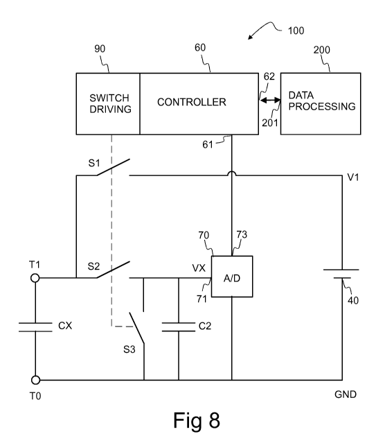
Fig. 8 shows a proximity detecting device 100, which may comprise a
capacitive sensor 20, switches S1, S2, S3, a tank capacitor C2, a
voltage supply 40, a reference voltage source 58, an analog-to-digital
(A/D) converter 70, and a controller 60.
The voltage supply 40 provides a voltage V1. The capacitive proximity
sensor 20 is represented by the unknown sensor capacitance CX.
The first node of the voltage source 40 is coupled to the first terminal
TO of the sensor capacitor CX. The second node of the voltage source
40 is coupled to the second terminal T1 of the sensor capacitor CX by
the switch S1. Thus, the sensor capacitor CX may be charged to
substantially the voltage V1 of the supply 40.
The terminal TO may also be connected to the ground GND. However,
this is not always necessary.
First, the tank capacitor C2 may be discharged by closing the switch
S3. Then, the switch S3 is opened and kept in the open state. The
sensor capacitor CX is charged by closing the switch S1, while the
switch S2 is in the open state. Then, the switch S1 is opened and
charge is transferred from the sensor capacitor CX to the tank
capacitor C2 by closing the switch S2. The transferred change
increases the voltage VX over the tank capacitor by a small amount.
CA 02693626 2010-01-08
WO 2009/007500 PCT/F12008/050379
17
The voltage VX of the tank capacitor is increased by closing and
opening the switches S1 and S2 consecutively several times e.g.
during a predetermined time period TFIX (Fig. 9).
Alternatively, voltage VX of the tank capacitor may be increased by
closing and opening the switches S1 and S2 consecutively several
times until the voltage VX reaches or exceeds a predetermined voltage
level Vref.
The voltage VX may be coupled to an input 71 of the A/D converter 70.
The output of the A/D converter 70 may be coupled to an input 61 of
the controller 60.
The switches S1, S2, S3 may be controlled by at least one switch
driving unit 90, which may be a separate component or incorporated in
the controller 60.
The driving unit 90 may be arranged to discharge the tank capacitor C2
by closing the switch S3 after the predetermined time period TF,x.
Alternatively, the driving unit 90 may be arranged to discharge the tank
capacitor C2 by closing the switch S3 when the voltage VX reaches or
exceeds a predetermined voltage level Vref.
The controller 60 may be arranged to count the number Nk of charge
transfer cycles, i.e. closing times of the switch S2 needed to change
the state of the comparator output. The controller 60 may be arranged
to send the counted number Nk to an external data processing device
200 via terminals 62, 201.
The counter number Nk, or further information dependent on said
counted number represents a measurement result.
Alternatively, or in addition, the controller 60 may be arranged to
determine the rate of change of the voltage VX during the charging of
CA 02693626 2010-01-08
WO 2009/007500 PCT/F12008/050379
18
the tank capacitor C2. The controller 60 may be arranged to determine
further information from the rate of change of the voltage VX.
The time period TFIX may be arranged to be short enough so as to
provide a substantially linear relationship between the count number Nk
and the capacitance value CX.
The reference voltage Vref may be arranged to be low enough so as to
provide a substantially linear relationship between the count number
and the capacitance value CX. Vref may be e.g. lower than or equal to
30% of the voltage V1 of the voltage supply 40
The data acquisition rate of the A/D converter 70 may be higher than or
equal to the switching frequency of the second switch S2 in order to
record the voltage value VX for each charge transfer step and in order
to capture the maximum number of data points for numerical signal
processing. However, the acquisition rate of the A/D converter 70 may
also be lower in order to simplify and speed up numerical signal
processing.
An analog low pass filter may be coupled before the input 71 of the A/D
converter 70 to further reduce noise.
Fig. 9 shows the timing chart for the device of Fig. 8. The first, the
second, and the third curves from the top show the states of the
switches S1, S2, and S3, respectively. The fourth curve shows
temporal evolution of the voltage VX of the tank capacitor C2.
The switch S3 is closed at the time t4,k_1 in order to discharge the tank
capacitor C2. The switch S3 may be kept closed for a predetermined
time in order to ensure that the tank capacitor C2 is discharged to a
sufficient degree.
The logical state 0 denotes an open switch and the logical state 1
denotes a closed switch. At least one of the switches S1, S2 should be
open during discharging of the tank capacitor C2.
CA 02693626 2010-01-08
WO 2009/007500 PCT/F12008/050379
19
The switch S3 is opened at the time tl,k and the sensor capacitor CX is
charged by closing the switch S1. S2 is in the open state. The switch
S1 is opened at the time t2,k and the switch S2 is closed in order to
transfer charge from the sensor capacitor CX to the tank capacitor C2.
The switches S1 and S2 are opened and closed alternately several
times until a fixed time period TF,x has been elapsed starting from the
time t2,k.
At the end of the time period TFIX, i.e. at the time t3,k, the final value Vk
of the voltage VX of the tank capacitor C2 may be recorded. The final
value Vk represents the measured value having an index k. The sensor
capacitance CX is now approximately inversely proportional to the final
value Vk.
The switch S3 is closed at the time t4,k in order to discharge the tank
capacitor C2 again.
A new charging and charge transfer sequence by using the switches
S1 and S2 is started again at the time t1 k+1 in order to determine the
next final voltage value Vk+1, i.e. in order to determine a new
measurement value.
Instead of the determining the final voltage Vk, the controller 60 may
also be arranged to determine a change of voltage VX during the
charging of the tank capacitor C2. The controller 60 may also be
arranged to determine the rate of change of voltage VX, or some other
parameter dependent on said rate of change during the charging of the
tank capacitor C2.
Referring to Fig. 10a, the voltage VX of the tank capacitor may have
noise bv. Electromagnetic noise may be e.g. originally coupled to the
plates 10a, 10b of the sensor 20 and to the wires of the sensor 20.
Typically, the most notorious noise components are at 50Hz (in
Europe) and at its harmonics due to the alternating mains voltage of
the electrical power network (at 60 Hz in the USA). The noise of the
CA 02693626 2010-01-08
WO 2009/007500 PCT/F12008/050379
sensor 20, i.e. the noise of the voltage of the sensor capacitor CX is
considerably reduced when charge is transferred from the sensor
capacitor CX to the tank capacitor, because the combination of the
switch S2 and the tank capacitor C2 acts as a low pass filter. However,
5 a part of the noise of the sensor capacitor CX is still carried over to the
voltage VX of the tank capacitor C2. Noise may also be coupled
directly to the measuring circuit of the device 100. Also the reference
voltage level Vref at the input of the comparator may have considerable
noise, as well.
The length of the time period Tk and/or the count number Nk is
determined by detecting the time when the voltage VX reaches or
exceeds the reference voltage level Vref. In other words, the length of
the time period Tk and/or the count number Nk may be measured by
determining the point CP1 where the voltage curve of VX touches or
intersects the reference voltage level Vref.
The noise causes uncertainty in the determination of the voltage VX of
the tank capacitor C2, and consequently a variation AT in the length of
the determined time period Tk, and/or a variation in the value of the
count number Nk.
The effect of the noise may be reduced if several voltage values are
taken into consideration instead of a single voltage value provided by
the A/D converter 70.
Referring to Fig. 10b, a line LIN1, which passes through zero voltage at
t2,k, may be fitted to two or more further voltage values MP. Thus, the
location of the intersection point CP1 may be interpolated or
extrapolated. CP1 is the intersection point of the line LIN1 and the
reference voltage level Vref. The line LIN1 may be fitted to substantially
all voltage values MP measured during a time period TFIX in order to
improve measurement accuracy. For example, least squares fitting
may be used to determiner the slope of the line LIN1. The slope of the
line LIN1 approximates the time derivative of the voltage VX of the tank
capacitor C2, i.e. the rate of change.
CA 02693626 2010-01-08
WO 2009/007500 PCT/F12008/050379
21
The length of the time period TFIX may be fixed and it may be
substantially shorter than a time period Tk which would be needed for
actually reaching a reference voltage level Vref. Thus, one may
determine the intersection point CP1, the time period Tk, and the count
number Nk by extrapolation. Consequently, the capacitance CX of the
sensor 20 may be determined at a higher rate than without
extrapolation.
The controller 60 may also be arranged to perform signal processing
operations needed for fitting and extrapolation.
The relationship between the voltage VX and time is not exactly linear.
Also an exponential curve may be fitted to the measurement points MP
instead of the line LIN1.
Instead of fitting and extrapolation, the controller 60 may also be
arranged to determine when an average VAVE of at least two voltage
values MP of the tank capacitor voltage VX exceeds a predetermined
reference voltage Vref. The reference voltage level Vref may also be
adaptively adjusted in order to ensure sufficient resolution and/or
sufficient sampling rate. Said adjustment may be made by the
controller 60 or the computer 200 based on a measured value provided
by a previous measurement cycle.
The controller 60 may also be arranged to determine a rate of change
of the tank voltage VX on the basis of a difference between a first
average value of a first group of points MP and a second average
value of a second group of points MP.
Referring to Fig. 11, a sensor array 20 may comprise an array of plates
10a, 10b, 10c, and 10d in order to detect the location of the object
BOD1. Each plate 10a, 10b, 10c, 10d may be connected to a
multiplexer 30 by conductors 11 a, 11 b, 11 c, 11 d. The multiplexer 30
may be arranged to couple each plate 10a, 10b, 10c, 10d sequentially
to the terminal T1. One or more of the adjacent plates may be
CA 02693626 2010-01-08
WO 2009/007500 PCT/F12008/050379
22
sequentially coupled to the other terminal TO, respectively. For
example, when the plate 10c is coupled to the terminal T1, the adjacent
plate 11 b may be coupled to the terminal T1 to establish a capacitive
sensor CX formed by the plates 10b and 10c.
The terminals TO and T1 of the multiplexer 30 may be coupled to the
measuring circuit as shown in Figs. 3 and 8.
The multiplexer 30 may be further arranged to communicate with the
controller 60 and/or with the data processor 200 in order to associate
the measured signal with the location of the currently activated sensor
plates, i.e. to indicate the location of the object BOD1.
Fig. 12a illustrates a sensor web W for monitoring electrically
conductive objects, for example the movement and location of a human
body. It is possible, for example, to use the web W for monitoring aged
and disabled people. Also possible applications include but are not
limited to the monitoring of jails and prisons, home and industrial
automation, vehicle airbag systems and other sensing applications.
The sensor web W comprises sequential electrically conductive areas
1. A conductor 2 connects the electrically conductive area 1 to an
output 3. The output 3 is provided with a connector. The parallel
conductors 2 extend linearly and form an angle a to the longitudinal
direction LD of the web W.
A piece of said web W may be used as a floor sensor.
A sensor array 20 may be a piece cut from a longitudinal web W. The
web W may comprise a plurality of plates 1, each having a conductor 2.
The conductor 2 of several plates 1 may be arranged to extend to a
connection area 3 at a cut end of the web W. Thus, it is easy attach the
measuring circuit or extension cables to the sensor 20, e.g. by using
crimp connectors.
The plates and the conductors of an uncut web W may be periodically
arranged on the substrate 5 such that a sensor array 20 may be
CA 02693626 2010-01-08
WO 2009/007500 PCT/F12008/050379
23
formed by cutting from the web W. In case of Fig. 12a, the sensor array
20 may comprise five or less plates 1, wherein the conductors 2 of said
plates extend to the connection area 3 at the end of the sensor 20.
Fig. 12b shows a cross-sectional view of the sensor web W (section A-
A in Fig. 12a). The sensor product comprises a substrate 5, electrically
conductive areas 1 which form sensor elements formed on the surface
of the substrate 5 and conductors 2 connecting the sensor elements to
an output 3. The electrically conductive areas 1 may, for example,
consist of etched copper.
The plates 1 and the conductors 2 are arranged on an electrically
insulating substrate 5. The plates 1 and the conductors 2 may be
covered with a protective layer 4 in order to prevent wear and electric
contact with the object BOD1.
The sensor 20 may also be implemented without the protective layer 4.
The sensor 20 may also be implemented upside down. The conductors
2 and the plates 1 may be on different sides of the substrate 5. The
sensor 20 may comprise further protective and/or electrically insulating
layers.
Electrically conductive areas and conductors may be die-cut from a
metal foil, and they may be laminated between two substrates, i.e.
between two superimposed webs.
Electrically conductive areas and their conductors may be located in
one layer, and optional RF loops and their conductors may be located
in another layer. In principle, it is possible to use different techniques,
e.g. etching, printing, or die-cutting, in the same product. For example,
the electrically conductive areas may be die-cut from a metal foil, but
their conductors may be etched. The electrically conductive areas and
their conductors may be connected to each other through vias.
The device 100 according to the invention may be used e.g. to monitor
the presence and/or movements of people in private houses, banks or
CA 02693626 2010-01-08
WO 2009/007500 PCT/F12008/050379
24
factories in order to implement an anti-theft alarm system. A network of
sensors 20 may be used to monitor the presence and/or movements of
people in department stores e.g. in order to optimize layout of the
shelves. The sensor may be used e.g. in hospitals or old people's
homes to detect patient activity and their vital functions. The sensor
may be used in prisons to monitor forbidden areas. The sensor may be
used for detecting movement of other large conductive bodies, such as
wheelchairs or aluminum ladders. The sensor may be used for
detecting movement of animals.
The sensor 20 may be installed e.g. in or on a floor structure. The
measuring circuit may be close to the sensor 20 so as to reduce noise.
The distance between the first plate 10a of the sensor 20 and the tank
capacitor C2 may be e.g. smaller than or equal to 0.5 m. The width of
the first plate 10a may be e.g. greater than equal to 10 times the width
of a conductor 2 which connects the first plate 10a to the measuring
circuit. The whole proximity detecting device 100 may be installed e.g.
on or in a floor structure so as to minimize the distance between the
sensor 20 and the tank capacitor C2. For example, the distance
between the tank capacitor C2 and the upper surface of the floor may
be smaller than or equal to 50 mm.
The distance from both plates 10a, 10b of a capacitive sensor C2 to
the tank capacitor C2 may be smaller than or equal to 0.5 m in order to
reduce noise.
Referring to Fig. 13, two capacitive sensors may be coupled to a
differential measuring circuit in order to reduce the effect of noise. In
certain cases it is probable that electromagnetic noise is coupled to
adjacent capacitive sensors in a substantially similar way. Thus, the
induced common-mode noise may be effectively eliminated by a
differential measurement, wherein the movement of an object BOD1 in
the vicinity of the sensors may cause a difference in the capacitances
of the two sensors.
CA 02693626 2010-01-08
WO 2009/007500 PCT/F12008/050379
A proximity detecting device 100 may comprise a first capacitive
sensor represented by a first sensor capacitance CXa, and a second
capacitive sensor represented by a second sensor capacitance CXb.
The device 100 may comprise a first sub-unit for determining the first
5 sensor capacitance CXa, said first sub-unit comprising switches S1a,
S2a, S3a, and a first tank capacitor C2a. The device 100 may comprise
a second sub-unit for determining the second sensor capacitance CXb,
said second sub-unit comprising switches S1 b, S2b, S3b, and a
second tank capacitor C2b. In addition, the device 100 may comprise a
10 voltage supply 40, differential amplifier 80, A/D converter 70, and
controller 60.
First, the switches S3a, S3b may be arranged to discharge the tank
capacitors C2a, C2b. Then, the first tank capacitor C2a may be
15 charged via the switches S1a, S2a, and via the first sensor capacitor
CXa as described in the context of Fig. 8. The second tank capacitor
C2b may be substantially simultaneously charged via the switches
S1a, S2a, and via the second sensor capacitor CX2 as described in the
context of Fig. 8. Consequently, the voltage VXa of the first tank
20 capacitor C2a increases, and also the voltage VXb of the second tank
capacitor C2b increases. Assuming that the object BOD1 is closer to
the first sensor represented by the sensor capacitance CXa than to the
second sensor represented by the sensor capacitance CXb, first
sensor transfers charge to the first tank capacitor C2a more effectively
25 than what is the case for the second sensor. Thus, the voltage VXa of
the first tank capacitor C2a increases at a higher rate than the voltage
VXb of the second tank capacitor C2b. The first tank capacitor CXa
may be coupled to a non-inverting input 81 of the differential amplifier
80. The second tank capacitor CXb may be coupled to a non-inverting
input 82 of the differential amplifier 80. Thus, the differential amplifier
80 may be arranged to amplify the difference VXa-VXb between the
voltages VXa, and VXb. The output 83 of the amplifier 80 may be
coupled to an input 71 of an A/D converter 70. The output 73 of the A/D
converter may be coupled to an input 61 of the controller 60.
CA 02693626 2010-01-08
WO 2009/007500 PCT/F12008/050379
26
The first node of the voltage source 40 is coupled to the first terminal
TO of the sensor capacitor CXa. The second node of the voltage
source 40 is coupled to the terminal T1a of the first sensor capacitor
CXa by the switch S1 a. Thus, the sensor capacitor CXa may be
charged to substantially the voltage V1 of the supply 40.
The first node of the voltage source 40 is coupled to the first terminal
TO of the sensor capacitor CXb. The second node of the voltage
source 40 is coupled to the terminal T1 b of the second sensor
capacitor CXb by the switch S1 b. Thus, the sensor capacitor CXb may
be charged to substantially the voltage V1 of the supply 40.
The terminal TO may also be connected to the ground GND. However,
this is not always necessary.
The switch drive unit 90 may be arranged to control the switches as in
case of Fig. 8. The controller 60 may communicate with a data
processor 200 via terminals 62, 201. The voltage supply 40 provides
the voltage V1.
The tank capacitors C2a, C2b may be discharged by closing the
switches S3a, S3b. Then, the switches S3a, S3b are opened and kept
in the open state. The sensor capacitor CXa is charged by closing the
switch S1a, while the switch S2a is in the open state. The sensor
capacitor CXb is charged by closing the switch S1 b, while the switch
S2b is in the open state. Then the switches S1a, S1b are opened and
charges are transferred from the sensor capacitors CXa, Cxb to the
tank capacitors C2a, C2b by closing the switches S2a, S2b. The
transferred charges increase the voltages VXa, VXb over the tank
capacitors.
The voltages VXa, VXb of the tank capacitors are increased by closing
and opening the switches S1a, S1b, S2a, S2b consecutively several
times.
CA 02693626 2010-01-08
WO 2009/007500 PCT/F12008/050379
27
The voltage VXa may rise at a rate AVa/dt. The voltage VXb may rise at
a rate AVb/dt. The voltages VXa, VXb increase at different rates
because the object BOD1 may be e.g. closer to the first sensor than
the second sensor. The difference AVa/dt-AVb/dt between the rising
rates represents a measurement value, which can be determined
and/or calculated from the output of the A/D converter 70.
A positive difference may indicate that an object BOD1 is closer to the
first sensor CXa, and a negative difference may indicate that the object
is closer to the second sensor CXb.
The differential amplifier 80 may be omitted if two A/D converters are
used substantially simultaneously (not shown in Fig. 13).
Figs. 14a and 14b show sensor arrays 20 suitable for use with the
device 100 of Fig. 13. Referring to Fig. 14a, the sensor array 20 may
comprise a first plate 10a, a second plate 10b, and a third plate 10c
disposed on a substrate 5. The first plate 10a is connected to the
terminal T1 a, the second plate may be connected to the terminal TO,
and the third plate may be connected to terminal T1 b.
The first plate 10a and the second plate 10b may together form a first
capacitive proximity sensor represented by a sensor capacitance CXa.
The second plate 10b and the third plate 10c may together form a
second capacitive proximity sensor represented by a sensor
capacitance CXb.
The terminals T1 a, Tlb and TO may be coupled to the device 100 as
shown in Fig. 13. The capacitance CXa is higher than the capacitance
CXb when the object BOD1 is closer to the plate 10a than to the plate
10c (assuming that the dielectric constant of the object BOD1 is greater
than one).
Referring to Fig, 14b, the sensor array 20 may comprise a first plate
10a, and a second plate 10b disposed on a substrate 5. The first plate
10a may be connected to the terminal Tla, and the second plate 10b
CA 02693626 2010-01-08
WO 2009/007500 PCT/F12008/050379
28
may be connected to the terminal T1 b. The sensor array 20 may
operated in combination with a conductive structure 22. The conductive
structure 22 may be e.g. earth, a large metal plate or water pipeline
system of a building. Thus the conductive structure 22 may be an
electrical ground GND. The terminal TO may be coupled to the
conductive structure 22, which in this case acts as capacitive element
of a capacitive sensor.
Now, a first capacitive sensor is formed between the first plate 10a and
the conductive structure 22. A second capacitive structure is formed
between the second plate 10b and the conductive structure 22.
The terminals T1 a, T1 b and TO may be coupled to the device 100 as
shown in Fig. 13. The capacitance CXa is higher than the capacitance
CXb when the object BOD1 is closer to the plate 10a than to the plate
10b (assuming that the dielectric constant of the object BOD1 is
greater than one).
The attainable resolution depends on the number of consecutive
charge transfer cycles needed to charge the tank capacitor C2 before
resetting (i.e. discharging). For example, a count number Nk or time
period Tk determined on the basis of 1024 charge transfer cycles
corresponds to a resolution of 10 bits. For example, a count number Nk
or time period Tk determined on the basis of 256 charge transfer cycles
correspond to a resolution of 8 bits
Referring back to Figs 3 and 8, the switches S1 and S2 may also be
bidirectional, and the voltage of the voltage supply 40 may also be
changed. The voltage V1 of the voltage supply may be changed to zero
or its polarity may even be reversed. Consequently, the tank capacitor
may also be discharged via the switches S1 and S2 and the sensor
capacitor CX back to the voltage supply. In that case it is not
necessary to operate the discharging switch S3, and it might even be
eliminated from the system. The count value Nk may be recorded both
during charging and discharging of the tank capacitor C2. Thus, the
sampling rate can be increased even further.
CA 02693626 2010-01-08
WO 2009/007500 PCT/F12008/050379
29
The device 100 may comprise one or more low-pass filters to reduce
noise. For example, an analog low-pass filter may be implemented
between the amplifier 80 and the A/D converter 70 in Fig. 13.
In many cases, it is not necessary to determine the absolute value of
the capacitance CX. It may be sufficient to detect changes in the value
of said capacitance CX.
Respiratory and cardiac functions cause periodic variations in the
spatial distribution of blood in human beings and animals, i.e. in the
object BOD1. These cause periodic variations in the capacitance of the
sensor 20. Thus, the device 100 may be used for monitoring cardiac
and/or respiratory function of human beings or animals. A person may
be lying on a sensor or sensor disposed on a floor or a bed. An
additional carpet or mattress may be positioned over the sensor 20, i.e.
between the sensor and the person.
The measurement of the capacitance is important in capacitive
sensors. The value of the capacitance is proportional to the measured
signal value, and may vary as a function of time. The accuracy and
speed of the capacitance measurement directly defines the properties
of the capacitive sensor or other application where the measurement of
the capacitance is important. In some cases, the capacitance to be
measured is very small, and the measurement is made by integrating a
very low-energy signal. The measurement is therefore sensitive to the
interference of electromagnetic radiation. The low energy means that
either the integration period or the signal value is very small, which
makes it difficult to sample and quantize the capacitance values to a
digital signal with a sufficiently high resolution. Sampling and
quantization would be needed to process the signal further e.g. with a
computer or a microcontroller.
Measuring the capacitance by using the switched capacitor method
makes it possible to integrate the low energy signal into a larger energy
signal before sampling and quantization. Therefore the measurement is
CA 02693626 2010-01-08
WO 2009/007500 PCT/F12008/050379
not so sensitive to interferences any longer. It is also possible to control
the measurement to optimize the resolution. The measurement method
according to the invention also introduces an analog low-pass filter into
the measurement circuit, further attenuating high frequency
5 interference signals.
The method and the device according to the invention may be
implemented by adding a known capacitor and processor-controlled
switches to the measuring circuit.
In the concept of switched capacitor circuits, a capacitor is connected
between two switches S1, S2. The switches S1 and S2 are opened
and closed in turns. The switches are preferably never closed at the
same time. In this kind of circuit, the capacitor will act like a resistance,
whose value is
Rc = 1~ (1)
.fSW
where fsw is the switching frequency of the switches and C is the
capacitance. Rc defines the relationship between a voltage over the
capacitor C and the current transferred by the capacitor C.
Switched capacitors may be used e.g. in analog signal processing,
since the resistance Rc can be adjusted by changing the switching
frequency fsW.
Referring back to Fig. 2, a switched capacitor circuit may comprise the
sensor capacitance CX and two switches S1 and S2. When the
switched capacitor circuit is operating, a known switching frequency fsw
may be used to open and close the first switch S1 and the second
switch S2 in such a way that when the first switch S1 is closed the
second switch S2 is open and vice versa. A known capacitor C2 is
charged through the switched capacitor circuit by closing the first
switch S1 to charge the sensor capacitance CX. After a certain time
period defined by the switching frequency fsw, the first switch S1 is
CA 02693626 2010-01-08
WO 2009/007500 PCT/F12008/050379
31
opened and the second switch S2 is closed to charge the known
capacitor C2 by moving charge from the sensor capacitor CX to the
known capacitor C2. The time constant of the formed RC-circuit may
be then measured, and it is proportional to the capacitance value of
CX.
The measured time constant may depend on three factors: the
switching frequency fsw, the capacitance of C2, and the loading voltage
V (i.e. the voltage level of the capacitor C2 attained after charge
transfer). Therefore, the measurement time and accuracy can be
adjusted to maximize resolution and to minimize the measurement
time. The adjustment can also be accomplished by software, making it
also possible to extend the measurement range, time or accuracy
during the measurement. Furthermore, the first-order low-pass filter,
formed by the RC-circuit, attenuates the high frequency electro-
magnetic disturbances considerably.
The proposed method may utilize two switches and the known
capacitance in addition to components used for a direct time constant
measurement of CX. Therefore, in many cases, the circuit is not too
complicated or expensive.
The purpose may be to measure the capacitance of the capacitive
sensor as accurately as possible (at an accuracy of more than 8 bits) at
minimum costs. The system may be capable of measuring capacitance
variations of a frequency of 0 to 40 Hz.
The magnitude of noise signals induced to the system (50 Hz and
multiples, as well as sampling jitter) is likely to be multiple in
comparison to the signal being measured.
A micro controller, whose properties are listed in table 1, may be used
in the experiments. Possible measuring parameters are listed in table
2.
Table 1. Properties of AtMega8L (trade mark) micro controller
CA 02693626 2010-01-08
WO 2009/007500 PCT/F12008/050379
32
Clock frequency 8 MHz
Program memory 8 kB Flash
Data memory 1 kB SRAM
Non-volatile data memory 512 B EEPROM
Timers 2 x 8b, 1 x 16b
ADC 1 x 10b
Analogue comparator 1
Digital I/O 23
Operating voltage 2.7V - 5.5V
Flash means flash memory, SRAM means static random access
memory, EEPROM means electrically erasable programmable read-
only memory, ADC means A/D converter, I/O means input/output, and
b means bit.
Table 2. Measuring parameters
Operating voltage Ve~ = 5V
Target voltage Vt=Vc
,c/3 = 1.7 V
Sensor capacitor 200 - 400 pF
Resistance 0.1 mS2
The switched capacitor measurement circuit was shown in Fig. 2.
During switching the switches S, and S2 are opened and closed
alternately, both on frequency fsw, and the capacitor C, operates like a
resistance in the switching. Thus, the capacitor C2 is charged little by
little. The flow resistance R. caused by CX depends on both the
capacitance CX and the switching frequency fsw according to the
following formula
1
Rc _ (2)
fsw CX
CA 02693626 2010-01-08
WO 2009/007500 PCT/F12008/050379
33
It is possible to determine the capacitance CX when C2 and fsw are
known. Since the capacitance of the known capacitor C2 and the
switching frequency fsw can be selected relatively freely, the charging
time of the known capacitor C2 can be selected as suitable.
The charging time tcHARGE may be calculated from the equation
tCHARGE = - ln 3 C2
CX (3)
fSW
When the charging time is known, and when it is known that a value x
of a counter received from the measuring device is a product of the
charging time tcHARGE and the clock frequency of the processor Fc,k:
x=t=FCLK, (4)
the capacitance CX of the sensor may be calculated from the value x of
the counter:
CX = -ln? FCLK C2 (5)
3 .fSW x
The resolution rt attainable with a switched capacitor switching can be
calculated from the formula:
rt = 20 = 1og10 - ln 3 f LK ~~ (6)
fs w
where Fc,k is the clock frequency of the processor (the frequency by
which the value x of the counter is increased). The switching frequency
fsw may be produced with, for example, by the PWM (pulse width
modulation) generator of the processor, in which case it will not use
CPU (central processing unit) time of the processor. The frequency of
performing the measurement (i.e. examining the status of an I/O port)
CA 02693626 2010-01-08
WO 2009/007500 PCT/F12008/050379
34
depends on how much processing resources the processor requires for
signal processing operations.
Fig. 7a shows the capacitance C2 as a function of the sampling
frequency. The sampling frequency is indicated on the horizontal axis
(abscissa). Fig. 7a shows what the ratio of the freely selectable
parameters may be when 12-bit resolution is desired for the measuring
accuracy.
One possible arrangement is that the switching frequency FSw = 500
kHz, clock frequency Fc,k = 8 MHz and C2 = 470 nF. With these
parameters it is possible to reach a sampling frequency slightly higher
than 100 Hz.
In the analysis of measuring accuracy, the focus is mainly on what
accuracy can be reached with the micro processor used. Analog
components and switches may also have an effect on the measuring
accuracy.
In the switched capacitor switching, at least the low pass filter formed
by the switched capacitor (CX) and the known capacitor C2 filter out
high frequencies, in which case the signal should not fold a great deal.
The cutoff frequency of the filter may be derived from the formula:
f 1 _ 1 CX
C - 2;rRC 2;c C2 fSW
The dependence of the cutoff frequency from the selected capacitance
is shown in Fig. 7b. The vertical axis shows the cutoff frequency. With
the above-listed component values (FSw = 500 kHz, Fc,k = 8 MHz, and
C2 = 470 nF), the cutoff frequency is approximately fc = 100 Hz. The
cutoff frequency cannot be selected freely, because the same
parameters also have an effect on the selection of desired measuring
accuracy. In addition, the filter thus formed is only of a first degree, and
its steepness is only around -6dB per octave.
CA 02693626 2010-01-08
WO 2009/007500 PCT/F12008/050379
A further analog low pass filter may also be connected to the circuit so
that harmful folding of the signal can be avoided.
Due to the analog filtering, it would be likely that the sampled signal
5 includes frequencies in a less interesting frequency band. Impulse-like
noise might thus be filtered out relatively well already before the
sampling. The same sampling jitter problem due to the variation of
sampling time as in a direct measurement of charging time might still
occur.
In the switched capacitor switching, an analog switching device is
required on both sides of the capacitor. For that purpose, e.g. analog
switches or FET transistors can be used. In view of operation of the
switching, it is important that their resistance when the switch is closed,
as well as the capacitance of the switch, is as low as possible. The
resistance may be reduced by increasing the area of the
semiconductor channel. Increasing the area, however, increases the
capacitance of the switch. Therefore, when seeking a small
capacitance, it may be needed to select a slightly larger resistance.
Analogue switching devices possibly suitable for switching, as well as
their key parameters, are listed in table 3.
Table 3. Resistances and capacitances of analog switching devices
Component Code Ron Capacitance
Analog switch MAX312CPE 6.5 C2 47 pF
Analog switch CD4066BE 470 C2 8 pF
Analog switch DG403DJ 50 C2 39 pF
Power MOSFET SFP9530 < 0.3 C2 160 pF
N-channel MOSFET 2N5457 > 1 kC2 3 pF
MAX312CPE, CD4066BE DG403DJ, SFP9530, and 2N5457 are
identification codes used by one or more component manufacturers.
RON means the resistance in the conducting state.
CA 02693626 2010-01-08
WO 2009/007500 PCT/F12008/050379
36
The resistance of the switching device is not a very critical factor,
because the charged capacitance is typically only around 200 to 400
pF. If the resistance of the switch does not rise much above a kilo-ohm,
the charging time of the capacitor when charging through the switch
still remains so small that a switching frequency of even 1 MHz can be
used. Frequencies higher than 1 MHz might cause radio interferences
On the other hand, the capacitance of the switching device may well
approach 50% of the capacitance of the sensor capacitor. Thus, the
capacitance of the switching device has a great effect on the
measuring result. Because of this, it is advantageous to select such a
switching device, whose capacitance is as low as possible, even if its
resistance would then be higher.
A switching circuit where the analogue switch DG403DJ is used is
shown in Fig. 5. DG403DJ includes an internal inverter, in which case
one switch is always open and another one closed. The other switches
require an external inverter circuit, with which the inverted control can
be input separately for one of the switches.
The operation of the measuring circuit may be analyzed e.g. by using a
computer together with a computer program. With this program, it may
be possible to print measured values onto the screen in real time. The
values may be received by a computer such as a PC from the micro
controller via a serial line. An example output (counter value) of the
measurement is shown in Fig. 6. The sampling frequency was
19.52Hz. The smallest sample number was 9670 and the largest
33991.
In the switched measuring method, the charge of a small sensor
capacitor may be transferred to a larger capacitor thousands of times
before its voltage rises to a level corresponding to the voltage of a
logical one. Therefore, the charging time can be measured at a high
resolution even with a low clock frequency. In addition, the measuring
circuit forms a low pass filter, which attenuates high frequency
interferences. In a direct measuring method, the interference would be
CA 02693626 2010-01-08
WO 2009/007500 PCT/F12008/050379
37
folded onto the sampled signal. Both the size of the loaded capacitor
and the switching frequency of the sensor capacitor have an effect on
the charging time. The switching frequency and therefore also the
charging time can be controlled by a computer program. The switched-
capacitor measuring method may significantly improve the level of the
measuring signal when compared to direct measurement of charging
time. The noise level of the signal may decrease significantly, and the
resolution of the measurement may increase e.g. to approximately 14
or 15 bits.
However, the switched-capacitor measuring mode has some
drawbacks as well. When the charging time of the tank capacitor
increases, also the highest attainable sampling frequency (data
acquisition rate) decreases. The theoretical maximum sampling
frequency is between 250 and 500 Hz, when using an 8 MHz
processor and 14 to 15-bit measuring accuracy. In practice, the
maximum sampling frequency may be e.g. 160 Hz. The switched-
capacitor measuring method also requires a circuit which is only a little
more complicated and expensive than in the direct measuring method.
By adjusting the capacitance of the tank capacitor and the switching
frequency, it is possible to change the measuring resolution, the
duration of the measurement and the cutoff frequency of the low pass
filter of the circuit. Unfortunately, the resolution, duration and cutoff
frequency cannot be set independently of each other. In practice, it is
possible to set the two most important ones: resolution and duration.
The cutoff frequency may remain high in practice, in which case the
noise signal might fold over the effective signal during sampling.
The invention can be utilized in a capacitive floor sensor. The
capacitance of the floor sensor is low which makes it difficult to
measure the capacitance accurately by using a cost-effective
microcontroller embedded in a floor sensor element. The proposed
method increases the measurement accuracy to about 12-14 bits when
compared to 7-bits of a direct time constant measurement. Utilizing this
CA 02693626 2010-01-08
WO 2009/007500 PCT/F12008/050379
38
invention, it may be possible to use an inexpensive, low-power
microcontroller in the measurement unit.
The cost and power consumption of the micro-controller can be
important, because it may be powered from a battery and embedded in
a floor sensor element.
The switched capacitor circuit has a large measurement range. The
floor sensors need to be capable of measuring both small
capacitances, to detect someone stepping on the element, and double
or triple capacitances, when someone is lying on the sensor. In both
cases, the sensor should advantageously be capable of measuring
capacitance changes which are likely to be only 1:1000 of the
maximum value.
The measurement range of a switched capacitor circuit may be
adjusted. When a person is walking over a floor sensor, the
capacitance of the sensor is e.g. only about 200 pF. However, when
somebody is lying on the sensor, its capacitance may increase e.g. to
400-500 pF. In this case, it may be necessary to rapidly change the
measurement range, in order to get improved measurement accuracy.
This is possible e.g. by changing the switching frequency or by
changing the loading capacitance by software.
The measurement time may be adjusted. In some cases, there may be
persons walking fast across a floor. In this case, the elements of the
floor may be rapidly scanned using low accuracy, so as to monitor the
fast movement. When a person is lying on the floor, a higher accuracy
may be required in order to monitor the breathing and the heartbeat of
the person. The measurement time can now be longer. The
measurement mode of the system can be adjusted to a slower but
more accurate state by choosing a higher tank capacitance or by
lowering the switching frequency.
The switched capacitor circuit may be calibrated automatically. When
the floor sensors are installed in various environments, their bare-
CA 02693626 2010-01-08
WO 2009/007500 PCT/F12008/050379
39
capacitance can be different from place to place. To measure
effectively in all kind of environments, the sensor needs to adjust the
measurement range suitable and to calibrate the measured values
using the bare-capacitance. The calibration is easier and more
effective when the measurement range can be changed by the
software.
A time constant may be interpreted to be a time it takes the system's
step response to reach 63.2% of its final (asymptotic) value, i.e. 36.8%
below its final value. When the capacitance is connected to a voltage
source through a series resistor, a time constant may be a time it takes
until the voltage over the capacitance has reached 63.2% of the
voltage of the voltage source.
Sampling means conversion of an analog signal to a digital signal.
Sampling method means a manner in which the analogue variable, e.g.
the charging time of the capacitor, is converted to a digital variable.
Measuring algorithm means the signal processing operations
performed on the sampled signal in order to separate the signal being
searched from noise and other interferences.
The word "comprising" is to be interpreted in the open-ended meaning,
i.e. a sensor which comprises a first electrode and a second electrode
may also comprise further electrodes and/or further parts.
For a person skilled in the art, it will be clear that modifications and
variations of the devices and the method according to the present
invention are perceivable. The particular embodiments and examples
described above with reference to the accompanying drawings are
illustrative only and not meant to limit the scope of the invention, which
is defined by the appended claims.