Note: Descriptions are shown in the official language in which they were submitted.
CA 02693811 2010-01-12
WO 2009/015324
PCT/US2008/071153
Docket No 070835 1
PATENT
SYSTEM AND METHOD TO REDUCE DYNAMIC RAM POWER CONSUMPTION VIA
THE USE OF VALID DATA INDICATORS
FIELD OF THE INVENTION
[0001] The present invention relates generally to the field of memory and
in
particular to a system and method for reducing dynamic RAM power consumption.
BACKGROUND
[0002] Solid-state dynamic random access memory (DRAM) is a cost-efficient
bulk
memory solution for many modern computing systems, including portable
electronic
devices. DRAM, including synchronous DRAM (SDRAM), offers a high bit density
and
relatively low cost per bit compared to faster, on-chip memory structures such
as
registers, static RAM (SRAM), and the like, and dramatically higher access
speeds
than electro-, magneto-, or optical-mechanical bulk storage such as hard
disks, CD-
ROMs, and the like.
[0003] Figure 1 depicts a logical view of a representative 512 Mbit DRAM
array
100. The array 100 is organized as a plurality of separately addressable banks
102,
104, 106, 108. Each bank is divided into a large number, e.g., 4096, of rows
110. Each
row 110 is divided into a plurality of columns (e.g., 512 columns), and each
column
includes a number of data bits, typically organized as bytes (e.g., 8 bytes).
Several
data addressing schemes are known in the art. For example, in Bank, Row,
Column
(BRC) addressing, a memory address may be interpreted as
31-26 25-24 23-12 11-3 2-0
Chip Bank Byte
Row select Column select
select select select
In an alternative addressing scheme such as Row, Bank Column (RBC) addressing,
the memory address may be interpreted as
CA 02693811 2010-01-12
WO 2009/015324
PCT/US2008/071153
Docket No 070835 2
PATENT
31-26 25-14 13-12 11-3 2-0
Chip Bank Byte
Row select Column select
select select select
[0004] DRAM memory arrays are volatile; data stored in a DRAM array must be
refreshed periodically to maintain its integrity. During a DRAM refresh
operation, a
large number of data storage locations are simultaneously read out of the
array 100
and recharged. Conventionally, DRAM arrays are refreshed row-by-row. That is,
a row
¨ or, in some implementations, the same row simultaneously in every bank ¨ is
selected and all data within the row are refreshed in a single operation. As
used herein,
the term "independently refreshable memory unit," or IRMU, refers to the
quantum of
data that is refreshed in a single refresh operation. The IRMU for a DRAM
array is
typically a row, although the present invention is not limited to row-by-row
refresh
operations.
[0005] Refresh operations directed to a IRMU are conventionally
interspersed with
memory accesses, and are timed such that the entire DRAM array is refreshed
prior to
any data being lost due to charge decay. Traditionally, the refresh addresses
¨ that is,
the address of each independently refreshable memory unit ¨ are supplied by a
memory controller, such as a processor, which specifies a refresh operation
through a
unique combination of control signals. Modern SDRAM components may include two
additional refresh modes: self-refresh and auto-refresh. In both modes, the
SDRAM
component includes an internal refresh address counter. Self-refresh is
utilized in many
systems, such as battery-powered electronic devices, that employ a "sleep"
mode to
conserve power. In self-refresh mode, the SDRAM component is not accessible to
store or retrieve data; however, the SDRAM performs refresh operations
internally to
ensure the integrity of stored data. In auto-refresh mode, the memory
controller
specifies a refresh operation, but does not provide a refresh address. Rather,
the
SDRAM component increments an internal refresh address counter, which provides
successive independently refreshable memory unit (e.g., row) addresses.
CA 02693811 2012-10-01
74769-2716
3
[0006] Each refresh operation consumes power as data are read from
the DRAM
array and recharged. However, particularly following power-on or a system
reset, most
memory storage locations in the DRAM array do not contain valid data.
SUMMARY
[0007] According to one or more embodiments disclosed and claimed
herein, an
indicator is maintained that indicates whether or not a refreshable segment of
memory
contains valid data. When a refresh operation is directed to the associated
memory, the
refresh operation is suppressed if the memory does not contain valid data.
Significant
power savings may be realized by suppressing refresh operations directed to
invalid
data.
[0008] One embodiment relates to a method of refreshing dynamic
memory. An
indicator is associated with each independently refreshable memory unit. Upon
writing
data to an independently refreshable memory unit, the associated indicator is
set to
reflect valid data. Only the independently refreshable memory units whose
associated
indicator reflects valid data stored therein are refreshed.
[0009] One embodiment relates to a DRAM component. The DRAM
component
includes a DRAM array operative to store data and organized as a plurality of
independently refreshable memory units. The DRAM component also includes a
plurality of indicators, each associated with an independently refreshable
memory unit
and indicating whether valid data is stored in the independently refreshable
memory
unit. The DRAM component further includes a controller receiving control
signals and
operative to inspect the indicators and to refresh only the independently
refreshable
memory units storing valid data.
CA 02693811 2012-10-01
=
74769-2716
3a
[0009a] According to one aspect of the present invention, there is
provided a
method of refreshing dynamic memory having a plurality of refreshable memory
units,
the method comprising: associating an indicator with each independently
refreshable
memory unit; upon writing data to an independently refreshable memory unit,
setting
the associated indicator of the independently refreshable memory unit to
reflect valid
data; upon freeing the independently refreshable memory unit from allocated
memory, setting the associated indicator of the independently refreshable
memory to
reflect invalid data; and refreshing only those independently refreshable
memory
units whose associated indicator reflects valid data stored therein.
[0009b] According to another aspect of the present invention, there is
provided
a DRAM component, comprising: a DRAM array operative to store data, the DRAM
array comprising a plurality of independently refreshable memory units; a
plurality of
indicators, each associated with an independently refreshable memory unit and
indicating whether valid data is stored in the independently refreshable
memory unit;
upon freeing an independently refreshable memory unit from allocated memory,
setting its associated indicator to reflect invalid data; and a controller
receiving control
signals and operative to inspect the indicators and to refresh only those
independently refreshable memory units whose associated indicator indicates
valid
data.
[0009c] According to still another aspect of the present invention, there
is
provided a computer readable medium storing statements and instructions for
use in
the execution in a computer of a method comprising the steps of: receiving a
request
from a task running on a processor to allocate memory to the task; allocating
memory
to the task from one or at least one independently refreshable memory unit in
the
DRAM array; in response to the allocating memory, setting an indicator
associated
with each of the at least one independently refreshable memory unit to direct
the
dynamic random memory not to suppress refresh operations directed to the at
least
one independently refreshable memory unit; receiving a request from the task
to free
the allocated memory; and in response to freeing the allocated memory, setting
the
CA 02693811 2012-10-01
74769-2716
3b
indicator associated with each of the at least one independently refreshable
memory
unit to direct the dynamic random memory to suppress refresh operations
directed to
the at least one independently refreshable memory unit.
[0009d] According to yet another aspect of the present invention,
there is
provided a DRAM component, comprising: a DRAM array operative to store data,
the
DRAM array comprising a plurality of independently refreshable memory units; a
plurality of means for storing indicators, each means for storing an indicator
associated with an independently refreshable memory unit and indicating
whether
valid data is stored in the independently refreshable memory unit; upon
freeing an
independently refreshable memory unit from allocated memory, setting its
associated
means for storing an indicator to reflect invalid data; and means for
receiving control
signals and operative to inspect the means for storing the indicators and to
refresh
only those independently refreshable memory units whose associated means for
storing an indicator indicates valid data.
BRIEF DESCRIPTION OF DRAWINGS
[0010] Figure 1 is a functional block diagram of data organization in
a DRAM
array.
CA 02693811 2010-01-12
WO 2009/015324 PCT/US2008/071153
Docket No 070835 4
PATENT
[0011] Figure 2 is a functional block diagram of data organization in a
DRAM array,
with a valid indicator or bit associated with each independently refreshable
memory
unit.
[0012] Figure 3 is a functional block diagram of an SDRAM component.
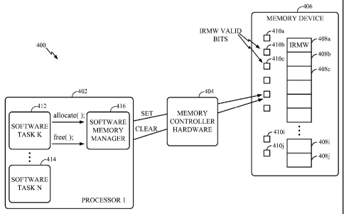
[0013] Figure 4 is a functional block diagram of a single-processor
computing
system.
[0014] Figure 5 is a functional block diagram of a multi-processor
computing
system.
[0015] Figure 6 is a flow diagram of a method of refreshing a DRAM array.
DETAILED DESCRIPTION
[0016] Figure 2 depicts a logical view of a DRAM array 200 organization
according
to one embodiment. The array 200 is logically organized as four banks 202,
204, 206,
208, each bank comprising 4096 rows. A representative row is depicted as 210.
In this
embodiment, a row 210 is the smallest independently refreshable memory unit.
Associated with row 210 in the array 200 is an indicator 211 reflecting
whether or not
the row 210 contains valid data. In the embodiment depicted, each indicator
211
comprises a single bit, also referred to herein as a valid bit, associated
with each row.
Figure 2 depicts sets of indicator bits 212, 214, 216, 218, each indicator bit
associated
with a row in banks 202, 204, 206, 208, respectively. In an embodiment where
the
smallest independently refreshable memory unit comprises a row spanning all
four
banks 202, 204, 206, 208, only one set of indicator bits 212 would be
required.
[0017] During a refresh operation, the indicator or valid bit, e.g.
indicator 211,
associated with the currently addressed independently refreshable memory unit,
e.g.
IRMU 210, is inspected. If the indicator bit is set, indicating the associated
IRMU
contains valid data, a refresh operation is performed on the IRMU to maintain
the data.
If the indicator bit is not set, indicating the associated IRMU does not
contain valid
data, in one embodiment the refresh operation is suppressed, conserving power
that
CA 02693811 2010-01-12
WO 2009/015324 PCT/US2008/071153
Docket No 070835 5
PATENT
would otherwise be consumed in refreshing the IRMU. Thus, only IRMUs that
contain
valid data will be refreshed, and IRMUs in the array that are in an
uninitialized or "don't
care" state are not refreshed. The refresh address may be supplied by a memory
controller, or may be generated by an internal address counter, such as during
auto-
refresh or self-refresh.
[0018] The indicator bits may be maintained in a variety of ways. In one
embodiment, indicator bits are stored in a fixed or programmable part of the
memory
array 200. In this case, the usable size of the array 200 is reduced by
0.003%. In
another embodiment, indicator bits are stored on the DRAM/SDRAM component in
memory other than the DRAM array 200, such as in a static RAM structure, in
registers,
or the like. In one embodiment, the IRMU valid indicator memory is accessed
via 2-
cycle sequence similar to Mode Register and Extended Mode Register access
sequences of SDRAM components.
[0019] Figure 3 is a functional block diagram of an SDRAM component 300
according to one embodiment. The SDRAM 300 includes a DRAM array 301,
organized as four banks 302, 304, 306, 308. Each bank includes row and column
decoders 312, 310. Sense amplifiers 314 provide read data from the DRAM array
301
to I/0 buffers 316. Write data from the I/0 buffers 316 passes through input
buffer 318
and is stored in a write data register 320 prior to writing into the DRAM
array 301.
[0020] Operation of the SDRAM component 300 is controlled by a state
machine
322. Bank and memory addresses are input to an address buffer 324 and stored
in an
address register 326, where they control the column pre-decoder and counter
circuit
328. The Mode Register 330 and Extended Mode Register 332 store mode selection
bits such as Column Address Strobe (CAS) delay, burst length, and the like,
which
control operation of the burst counter 334 and the data out control circuit
336.
[0021] A refresh logic and timer circuit 338 receives IRMU addresses from
an
internal counter 340, and IRMU valid bits from IRMU valid memory 342. The
refresh
logic outputs IRMU addresses to a row pre-decoder 344. Note that while the
IRMU
CA 02693811 2010-01-12
WO 2009/015324 PCT/US2008/071153
Docket No 070835 6
PATENT
valid memory 342 is depicted in Figure 3 as functional block separate and
apart from
the DRAM array 301, the memory physically dedicated to the storage of IRMU
valid
indicators may be part of the DRAM array 301, or may be separate DRAM, SRAM,
registers, or other memory.
[0022] In one embodiment, the SDRAM component 300 automatically monitors
write addresses, and sets an IRMU valid indicator corresponding to the IRMU to
which
each write operation is directed. The refresh logic 338 then inspects the IRMU
valid
memory 342 upon each refresh operation, and suppresses refresh cycles directed
to
any IRMU that does not contain valid data. This minimizes the power
consumption of
the SDRAM component 300, but does not require any refresh-suppression
knowledge
or participation by a memory controller or a processor. The major power
savings are
likely to occur following power-on or reset, when the DRAM array 301 is mostly
empty
of valid data. As the memory controller writes data to more IRMUs in the DRAM
array
301, more IRMU valid bits are set, and fewer refresh cycles are suppressed. In
this
embodiment, the IRMU memory 342 is automatically cleared as part of the SDRAM
component 300 initialization following power-up or reset. This embodiment
allows
system designers to take advantage of the lower power consumption of the SDRAM
component 300, while utilizing existing memory controllers and software that
do not
include sophisticated memory management functionality.
[0023] In one embodiment, the IRMU memory 342 may be cleared by a command
from the memory controller, such as a predefined Mode Register 330 or Extended
Mode Register 332 write operation or bit pattern. This embodiment allows for
reduced
SDRAM component 300 power consumption following a soft (i.e., software-
initiated)
reset, but requires that the memory controller issue an IRMU memory 342 clear
command.
[0024] Figure 4 depicts a computing system 400 that controls and reduces
DRAM
power consumption. The system 400 includes a memory controller such as a
processor
402, memory controller hardware 404 (which may be integrated with the
processor
CA 02693811 2010-01-12
WO 2009/015324 PCT/US2008/071153
Docket No 070835 7
PATENT
402), and a memory device such as SDRAM component 406. A DRAM array within the
SDRAM component 406 is logically divided into independently refreshable memory
units 408a, 408b, 408c, ... 408j. Associated with each IRMU is an IRMU valid
indicator
such as a bit 410a, 410b, 410c, ... 410j, which indicates whether the
associated IRMU
contains valid data.
[0025] A plurality of software tasks 412, 414 execute on the processor 402.
Each
software task may allocate memory for data storage, and may free up memory no
longer needed. A Software Memory Manager 416 is a software module that manages
memory for the processor 402. The Software Memory Manager 416 receives memory
"allocate" and/or "free" requests from software tasks 412, 414. In response,
the
Software Memory Manager 416 allocates memory to and from the tasks 412, 414,
maps the allocated memory to one or more independently refreshable memory
units
408a, 408b, 408c, ... 408j (e.g., rows), and sets and clears the corresponding
IRMU
valid indicators 410a, 410b, 410c, ... 410j to reflect the status of data
currently in the
IRMUs 408a, 408b, 408c, ... 408j. In one embodiment, the actual memory
controller is
an independent hardware element 404; in another embodiment, the memory
controller
functionality is integrated into the processor 402. The SDRAM component 406
suppresses all refresh operations directed to IRMUs 408a, 408b, 408c, ... 408j
that
contain invalid data.
[0026] Figure 5 depicts a multiprocessor system 500 that controls memory
allocation and minimizes SDRAM power consumption. Processors 502, 504
communicate with each other and with memory controller hardware 508 across a
system bus 506. The bus 506 may also be implemented as a switching fabric, a
crossbar switch, or the like, as known in the art. One or more software tasks
503, 516,
518 execute on the processors 502, 504. A system-wide Software Memory Manager
520 executes on one processor 504, allocating memory to and from all software
tasks
503, 516, 518 executing in the system. Any software task 503 executing on a
processor 502 may send memory allocate and free requests to the Software
Memory
CA 02693811 2010-01-12
WO 2009/015324 PCT/US2008/071153
Docket No 070835 8
PATENT
Manager 520 across the bus 506. As described above, the Software Memory
Manager
520 allocates memory to and from the tasks 503, 516, 518, maps the allocated
memory
to one or more independently refreshable memory units 512a, 512b, 512c, ...
512j, and
sets and clears the corresponding IRMU valid indicators 514a, 514b, 514c, ...
514j via
the memory controller hardware 508 to reflect the status of data currently
stored in the
IRMUs 512a, 512b, 512c, ... 512j. The SDRAM component 510 suppresses refresh
operations directed to IRMUs 512a, 512b, 512c, ... 512j that contain invalid
data.
[0027] In conventional refresh mode, auto-refresh mode, or self-refresh
mode, the
SDRAM component 300, 406, 510 compares refresh addresses (supplied by a memory
controller or an internal counter) to IRMU valid memory 342, 410, 514, and
suppresses
refresh operations directed to IRMUs 408, 512 that do not contain valid data.
In one
embodiment, in which a Software Memory Manager 416, 520 actively manages
memory and sets/clears IRMU valid bits 410, 514, the system may further
optimize
memory refreshing and minimize power consumption by dynamically suppressing
refresh commands to IRMUs as physical memory is freed from allocation to a
software
task and returned to the "pool," in which case its data contents are not
relevant.
[0028] In conventional refresh mode, the Software Memory Manager 416, 520
may
provide refresh addresses only to IRMUs 408, 512 that contain valid data. In
auto-
refresh or self-refresh mode, the SDRAM component 300, 406, 510 may "skip"
invalid
memory by incrementing its refresh address counter to the next IRMU 408, 512
containing valid data, following each refresh operation. In either case, the
memory
controller 404, 508 may increase the delay between refresh operations, such
that only
the IRMUs 408, 512 that contain valid data are all refreshed with the maximum
refresh
period. In this embodiment, no refresh commands are suppressed by the SDRAM
component 300, 406, 510. This further optimizes power consumption (and reduces
bus
congestion) by avoiding unnecessary memory command cycles, and reduces the
delay
refresh commands impose on ongoing memory accesses.
CA 02693811 2010-01-12
WO 2009/015324 PCT/US2008/071153
Docket No 070835 9
PATENT
[0029] Figure 6 depicts a method 600 of a refreshing DRAM according to one
or
more embodiments. Upon initialization, all IRMU indicators are cleared (block
602). The
methods then checks whether a refresh operation is to be performed (block
604). In a
traditional refresh mode, a refresh operation is indicated by control signals
sent to the
DRAM component from a memory controller, and the IRMU to be refreshed is
indicated
on the address bus. In auto-refresh mode, the refresh operation is commanded
by a
memory controller, and an internal counter provides an IRMU refresh address.
In self-
refresh mode, expiration of a refresh timer indicates a refresh operation is
required,
and an internal counter provides the IRMU address.
[0030] If a refresh operation is indicated (block 604), the IRMU indicator
associated
with the current IRMU address (such as, for example, a row address) is
inspected
(block 606). If the IRMU indicator indicates that the IRMU contains valid data
(block
608), a refresh operation is performed on the addressed IRMU (block 610). If
the IRMU
indicator indicates that the IRMU does not contain valid data (block 608), the
refresh
operation is suppressed, saving the power that would otherwise be expended by
refreshing invalid (or "don't care") data.
[0031] In self-refresh mode, the SDRAM component waits at block 604 for the
next
expiration of the refresh address counter. In other refresh modes, if a
refresh operation
is not commanded (block 604), the DRAM (or SDRAM) component executes read,
write, and/or register access operations as commanded by a memory controller
(block
612). In one embodiment, where a memory management software module allocates
and frees memory blocks, the memory or register access operations may include
operations directed to IRMU memory ¨ reading, setting, and clearing the IRMU
indicators. In one embodiment, an IRMU indicator is automatically set upon a
write
operation directed to the associated IRMU (block 614). In this embodiment, the
IRMU
indicators are only clear upon initialization (block 602), but may provide
significant
power savings until valid data is written at least once to many IRMUs.
CA 02693811 2010-01-12
WO 2009/015324 PCT/US2008/071153
Docket No 070835 10
PATENT
[0032] By applying a software paradigm of memory management ¨ where memory
is only relevant when it is allocated to a task and assumes a "don't care"
state prior to
allocation or after being freed ¨ to the physical refresh operations of a DRAM
array,
significant power savings may be realized by eliminating unnecessary refresh
operations directed to segments of memory that do not hold valid data. In one
embodiment, the tracking of valid data, by setting associated IRMU bits, is
automatic.
In this embodiment, the power-saving benefits of the present invention are
available in
systems with no software memory management or knowledge of the ability to
selectively suppress refresh operations. In other embodiments, direct control
of the
IRMU memory allows for sophisticated memory management and maximum power
savings.
[0033] As used herein, the term "independently refreshable memory unit," or
IRMU,
refers to the quantum of data that is refreshed in a single refresh operation.
The IRMU
for a DRAM array is typically a row, although the present invention is not so
limited. As
used herein, the term "set" refers to writing data to an IRMU indicator to
indicate that
valid data is stored in the associated IRMU, regardless of the value of the
data (e.g., 0
or 1, or a multi-bit pattern). "Clear" refers to writing data to an IRMU
indicator to indicate
that valid data is not stored in the associated IRMU, regardless of the value
of the data
(e.g., 0 or 1, or a multi-bit pattern). As used herein, "DRAM array" refers to
a dynamic
random access memory array, which stores data in both DRAM and SDRAM
integrated
circuit components. As used herein, the scope of the terms "DRAM" alone or
"DRAM
component" include both asynchronous DRAM memory components and SDRAM
components. As used herein, the term "allocate" refers to assigning a range of
memory
addresses to a software task, and the term "free" refers to returning
previously
allocated memory addresses to a pool of unallocated memory.
[0034] Although the present invention has been described herein with
respect to
particular features, aspects and embodiments thereof, it will be apparent that
numerous
variations, modifications, and other embodiments are possible within the broad
scope
CA 02693811 2010-01-12
WO 2009/015324 PCT/US2008/071153
Docket No 070835 11
PATENT
of the present invention, and accordingly, all variations, modifications and
embodiments are to be regarded as being within the scope of the invention. The
present embodiments are therefore to be construed in all aspects as
illustrative and not
restrictive and all changes coming within the meaning and equivalency range of
the
appended claims are intended to be embraced therein.