Note: Descriptions are shown in the official language in which they were submitted.
CA 02694309 2015-07-30
MULTIPLE FUNCTION DIGITAL OPTICAL SWITCH
Background
[0002] As the quantity and speed of data communications over fiber optic
systems rapidly
increases due to the growing demand from Internet usage and other
communications,
improved all-optical switching systems are of increased interest to overcome
the high cost
and slow switching speeds of conventional switches. These conventional
switches include,
for example, various mechanical switches, electro-optic switches, and thermo-
optic
switches. In particular, the increased complexity and cost of switching
systems that involve
switching from an optical signal to an electrical signal and then back to an
optical signal
have increased the level of interest in improved all-optical switches.
[0003] An all-optical switch provides switching of an optical signal from one
input path to a
selected one of a plurality of different output paths without any intermediate
conversion of
the optical signal to an electrical signal. This is typically accomplished by
applying an
electrical signal to a switchable element to cause the optical signal to be
selectively
switched. These electro-optic switches are responsive to the electrical signal
to selectively
switch the light of the optical signal from the input path to the selected one
of the output
paths.
[0004] A variety of approaches are known for making all-optical optical
switches, such
as, for example, described in 6,687,431, 6,661,948, 6,625,346, and 6,549,699.
The
switchable element in many of these devices is a Micro-Electromechanical
System (MEMS)
optical element such as a MEMS mirror. The MEMS mirrors may be individually
controllable and movable, e.g., pivotable (or rotatable) under analog (or
continuous)
control, such that, upon reflection, optical wavelengths are directed from one
or more
input ports into selected ones of the output ports. In this way, the optical
switch may be
used to selectively couple the wavelengths between the input and output ports
of
-1-
CA 02694309 2010-01-22
WO 2009/015139
PCT/US2008/070751
the system. However, a number of problems arise when such MEMS mirrors
operating in
an analog manner are used in an optical switch. For example, to avoid
instability from
mirror structure resonance a means for sensing the precise position of each
MEMS mirror
may need to be integrated with the MEMS device, which can be difficult and
complex to
achieve. In addition, switching individual MEMS elements into a MEMS device
can
cause disturbances in neighboring MEMS elements. In particular, switching MEMS
mirrors in a MEMS array has been found to cause an aerodynamic coupling with
other
mirrors in the array that can disturb mirrors that are intended to remain
static. The
position of the MEMS mirrors can also drift because the mirrors are generally
actuated by
a relatively weak electrostatic force that requires a large voltage. The large
voltage can
cause charging that also disturbs the position of the mirrors. All of these
effects become a
more significant problem when these devices perform dynamic gain equalization
by off-
axis alignment of the free space beam as it is coupled into an output port.
This technique
requires in a much tighter tolerance in the mirror positoning because the
attenuation
sensitivity as a function of angular positioning level increases nonlinearly
as off-axis
alignment is extended to achieve higher attenuation levels. The higher
sensitivity is the
reason complex servo-loops and expensive mirror position sensing systems are
disclosed
as desirable for this technology.
[0005] Digital mirror arrays solve many of the problems with their analog
counterparts,
and a number of such arrays have become available which include an integrated
monolithic switching structure. These devices use relatively low voltages to
provide
individual mirror elements that can be selectively switched between two or
more
positions with high precision and stability. One class of such digital mirror
arrays are
spatial light modulators, often referred to as digital micromirror displays or
devices
(DMDs). Typically, a DMD consists of an array of tiny mirrors (typically,
several million
per square inch), wherein the angular position of each mirror element is
individually
controllable between at least two positions that are angularly offset from one
another by
approximately 10 to 20 degrees, for instance. A mirror base is located behind
the mirror
elements. The individually addressable mirror elements are tiltably mounted on
mechanical hinges, and typically the array of mirror elements overlays a layer
of
controlling circuitry in the mirror base, all of which is mounted on a
semiconductor chip.
The mirror face of the DMD is composed of a generally rectangular grid array
of
-2-
CA 02694309 2015-07-30
rectangular or square mirror elements. A typical mirror element is about 16
micrometers
square, and the individual elements are separated from one another by a
distance of about 1
micron. Individually controlled tilting of the mirror elements in the array
around at least one
axis allows energy that is reflected from the mirror face to be formed into a
predetermined
pattern. Further, the mirror face can be substantially instantaneously
reconfigured in response
to digital signals to form a different pattern. Such reconfiguration can
generally be achieved in
about 25 microseconds or less.
[0006] Optical switches incorporating DMDs are known and disclosed, for
example, in U.S.
Patent Nos. 6,295, 154, and 7,203,398 and U.S. Appl. Serial Nos. 2003/0164959
and
2002/0034356. These switches suffer from a number of limitations in extending
the devices to
higher levels of functionality to support multiple wavelengths or colors or
light on each port,
larger numbers of switching ports, or additional functionality such as
independent control of
the optical power level during switching.
[0007] Accordingly, it would be advantageous to provide a multiple function
DMD switching
device that is capable of performing multiple optical processing functions In
particular, it
would be advantageous to provide a device that integrates a lxN switch (where
N>1) that can
control the power levels directed to multiple output ports in a cross-talk
free manner.
Summary
[0007a] Certain exemplary embodiments can provide a multiwavelength switch,
comprising:
at least one optical input for receiving an optical beam; at least two optical
outputs; a
dispersion element receiving the optical beam from the optical input and
spatially separating
the optical beam into a plurality of wavelength components; a collimating
element for
collimating the plurality of wavelength components; and an actuatable optical
arrangement
receiving the collimated plurality of wavelength components from the
collimating element,
said actuatable optical arrangement including a digital micromirror device
(DMD) from which
at least one particular wavelength component is reflected at least once off of
a first portion
and at least once off a second portion of the DMD before being directed to a
selected one of
optical outputs, said second portion of the DMD being different from the first
portion of the
DMD.
-3-
CA 02694309 2016-03-18
,
[0007b] Certain exemplary embodiments can provide an optical switch,
comprising: at least
one optical input for receiving an optical beam; at least three optical
outputs; a collimating
element for collimating the optical beam; and an actuatable optical
arrangement receiving the
collimated optical beam, said actuatable optical arrangement including a
digital micromirror
device (DMD) from which the optical beam is reflected at least once off of a
first portion and
at least once off a second portion of the DMD before being directed to any
selected one or
more of the optical outputs, said actuatable optical arrangement having an
array of
individually actuatable mirror elements selectively positionable in any of
three states for
reflecting the optical beam, said second portion of the DMD being different
from the first
portion of the DMD.
[0007c] Certain exemplary embodiments can provide a method for directing
wavelength
components of an optical beam from an input port to at least one output port,
comprising:
receiving the optical beam at the input port; spatially separating the
wavelength components
of the optical beam; collimating the spatially separated wavelength
components; directing the
collimated wavelength components onto a digital micromirror device (DMD);
selectively
actuating individual mirror elements of the DMD to selectively direct
individual ones of the
wavelength components to at least one optical element that redirects the
individual
wavelength components back to the DMD; selectively actuating individual ones
of the mirror
elements onto which the individual wavelength components have been redirected
a second
time such that at least some of the individual wavelength components are
directed to at least
one selected output port.
[0007d] Certain exemplary embodiments can provide a method for directing
wavelength
components of an optical beam from an input port to at least one output port,
comprising:
receiving the optical beam at the input port; spatially separating the
wavelength components
of the optical beam; collimating the spatially separated wavelength
components; directing the
collimated wavelength components onto a digital micromirror device (DMD);
selectively
actuating individual mirror elements of the DMD to determine at least one
output port to
which individual wavelengths are to be independently directed; directing the
individual
wavelength components back to the DMD prior to directing them to the at least
one output
port to selectively attenuate one or more of the individual wavelength
components.
-3a-
CA 02694309 2016-03-18
[0007e] Certain exemplary embodiments can provide an optical switching
apparatus,
comprising: at least two independently operable optical switches, including:
at least one first
optical input and two first optical outputs associated with a first of the
optical switches for
selectively switching a first optical beam; at least one second optical input
and one second
optical output associated with a second of the optical switches for
selectively switching a
second optical beam; a dispersion element receiving the first and second
optical beams from
the first and second optical inputs and spatially separating the first and
second optical beams
into a first and second plurality of wavelength components, respectively; a
collimating
element for collimating the first and second plurality of wavelength
components; and an
actuatable optical arrangement receiving the first and second collimated
plurality of
wavelength components, said actuatable optical arrangement including a digital
micromirror
device (DMD) from which the wavelength components of the first and second
plurality of
wavelength components are each reflected at least once off of a first portion
and at least once
off a second portion of the DMD before being directed to a selected one of
first optical
outputs and the second optical output, respectively, said second portion of
the DMD being
different from the first portion of the DMD.
[0007f] Certain exemplary embodiments can provide a multiwavelength switch,
comprising:
at least two optical inputs for receiving optical beams; at least two optical
outputs; a
dispersion element receiving the optical beams from the optical inputs and
spatially separating
each of the optical beams into a plurality of wavelength components; a
collimating element
for collimating the plurality of wavelength components of each optical beam;
and an
actuatable optical arrangement receiving the collimated plurality of
wavelength components
from the collimating element, said actuatable optical arrangement including a
digital
micromirror device (DMD) from which at least one wavelength component is
reflected at
least twice off of a first set of different portions of the DMD to perform a
first function and
another wavelength component is reflected at least twice off of a second set
of different
portions of the DMD to perform a second function different from the first
function, said first
set of different portions being different from the second set of portions of
the DMD, wherein
the first function and the second function are performed independently and
simultaneously.
-3b-
CA 02694309 2015-07-30
100081 In accordance other embodiments, a multiwavelength switch is provided.
The switch
includes at least one optical input for receiving an optical beam and at least
two optical
outputs. A dispersion element receives the optical beam from the optical input
and spatially
separates the optical beam into a plurality of wavelength components. A
collimating element
is provided for collimating the plurality of wavelength components. An
actuatable optical
arrangement receives the collimated plurality of wavelength components from
the collimating
element. The actuatable optical arrangement includes a digital micromirror
device (DMD)
from which at least one wavelength component is reflected at least twice
before being
directed to a selected one of optical outputs.
-3c-
CA 02694309 2010-01-22
WO 2009/015139
PCT/US2008/070751
Brief Description of the Drawings
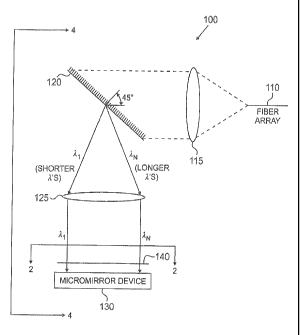
[0009] FIG. 1 shows a first side view of one embodiment of a wavelength
selective
switch constructed in accordance with the present invention.
[0010] FIG. 2 shows a plan view of the surface of the micromirror device on
which the
wavelengths are incident, taken along line 2-2 in FIG. 1.
[0011] FIG. 3 is a perspective view of two mirror elements, which are tiltably
mounted so
that they can tilt about axis.
[0012] FIG. 4 is a second side view of the wavelength selective switch taken
along line 4-
4 in FIG. 1.
[0013] FIGs. 5a and 5b show light paths being reflected off individual mirror
elements.
[0014] FIG. 6 is a side view of another embodiment of the switch taken along
lines 4-4 in
FIG. 4.
[0015] FIG. 7 shows the switch of FIG. 4 configured as a 1x2 switch with an
opitical
channel monitor (OCM).
Detailed Description
[0016] As detailed below, a wavelength selective switch that employs a DMD is
provided. In contrast to the switches described above, the wavelength
selective switch
described herein includes a dispersive element to separate the different
wavelengths of a
wavelength division multiplexed (WDM) or dense wavelength division multiplexed
(DWDM) signal, thereby enabling the switching of multiple wavelengths from
each port.
In addition, the switch can perform other functions in addition to or as an
alternative to
optical switching. For example, unlike the aforementioned switches, when the
switch
described herein is configured as a lxN switch with N>l, it can simultaneously
perform
dynamic gain equalization or power control on a per wavelength basis without
undesirable inter-port crosstalk.
[0017] It should be noted at the outset that the wavelength selective switch
described
below operates in a symmetric manner so that any wavelength components
directed to
any of the output ports can be alternatively directed to any of the input
ports.
Accordingly, one of ordinary skill in the art will recognize that the
switching paths are
reciprocal, and thus the terms input and output as used herein are not limited
to elements
that transmit an optical signal or wavelength component in a single direction
relative to
-4-
CA 02694309 2010-01-22
WO 2009/015139
PCT/US2008/070751
the switch. In other words, when light enters the device from any so-called
output port,
this output port serves as an input port, and similarly, any so-called input
port can equally
serve as an output port.
[0018] FIG. 1 shows a first side view of one embodiment of a wavelength
selective
switch 100 constructed in accordance with the present invention. While the
switch may be
employed in connection with any optical wavelengths, it is particularly
suitable for use in
connection with optical wavelengths in the C-band (wavelengths between about
1525 to
1565 nm) or the L-band (wavelengths between about 1565-1625 nm). The switch
includes an array 110 of parallel input/output optical ports (e.g., fibers) in
the plane
coming out of the page, only one of which is visible in FIG. 1. A collimating
lens 115 is
positioned to receive light exiting from the fiber array 110. The collimating
lens 115 is
centered about the optical axis extending from the middle fiber in fiber array
110. In this
way light exiting the fibers in the fiber array 110 is collimated by lens 115.
The
collimated light is then incident upon a transmission grating 120, which
spatially
separates the light into its component wavelengths 4 4 2,3, - 4 and directs
them
through a second lens 125. Lens 125 performs different functions in the two
axes of the
lens plane. In the plane of the page in FIG. 1, the lens collimates the
dispersed
wavelengths 2,1 through 2,1\T. In the plane out of the page the lens focuses
the collimated
beam onto the surface of the micromirror device 130. The result is a stripe of
spatially
separated wavelengths that are collimated along the axis of dispersion, and
focused
perpendicular to that axis, where the stripe is directed between mirror strips
140 (only
one of which is visible in FIG. 1) and onto the surface of a micromirror
device 130.
[0019] FIG. 2 shows a plan view of the surface of the micromirror device 130
on which
the wavelengths are incident, taken along line 2-2 in FIG. 1. The mirror face
of
micromirror device 130 is populated with thousands of miniature, tiltable,
individually
controllable mirror elements, typical ones of which are indicated at 140 and
145. Each
mirror element typically has dimensions on the order of microns. For example,
one
particular such micromirror device 130 is a 768x1024 array of individually
controllable
mirror elements. Each mirror element is a square about 16 microns on each side
and
rotates about an axis parallel to the plane of the device 130. As indicated in
FIG. 2 by
dashed line 150, the axis of the mirror elements extends diagonally from one
corner to the
opposite corner of each mirror element.
-5-
CA 02694309 2010-01-22
WO 2009/015139
PCT/US2008/070751
[0020] Mirror strips 1401 and 1402 ("mirror strips 140") are situated over the
surface of
the micromirror device 130 and extend in a direction parallel to the axis 150.
The mirror
strips 140 can be fabricated directly on the lower surface of a transparent
window or
substrate using conventional lithographic or other techniques. The substrate
can be
integrated with the micromirror device 130 to form a single optical assembly.
An anti-
reflective coating may be applied to the upper surface of the window to reduce
back
reflections. Likewise, an anti-reflective coating may be applied to the
nonreflective
portions of the lower surface between the individual mirror strips.
[0021] FIG. 3 is a perspective view of mirror elements 141 and 145, which are
tiltably
mounted so that they can tilt about axis 150. The unactuated surface 50 of
individual
mirror element 141, and the surface 52 of individual mirror element 145
normally lie in
the same plane, which can be referred to as the off or float state of the
mirror elements.
By the application of a controlling force to effect the movement of, for
example, support
member 48, surface 52 can be tilted around axis 150 out of the common plane.
If support
44 holds element 141 in its original position (i.e. its float state), light
incident on surface
50 will be reflected to a different location than light incident on surface
52. Micromirror
devices are well known, commercially available components and thus details
concerning
their structure and fabrication need not be discussed further.
[0022] Micromirror devices such as micromirror device 130 are generally
operated in one
of two modes of operation. The first mode of operation is an analog mode,
sometimes
called beam steering. In this mode of operation the address electrodes, which
control the
rotation of the individual mirror elements about their respective axes, is
charged to a
voltage corresponding to the desired deflection of the mirror. Light striking
the
micromirror device is reflected by the mirror at an angle determined by the
deflection of
the mirror. The second mode of operation is a digital mode. When operated
digitally, each
mirror element is fully deflected in either of the two directions about its
axis. That is, each
mirror element can be positioned in one of three states: two states in which
the mirror
element are tilted in opposite directions from one another and the off or flat
state. Digital
operation uses a relatively large voltage to ensure the mirror is fully
deflected. For
purposes of illustration the present invention will be described in terms of a
micromirror
device that operates in a digital mode. Such a micromirror device may be
conveniently
referred to as a digital micromirror device (DMD). In some embodiments of the
invention
-6-
CA 02694309 2010-01-22
WO 2009/015139
PCT/US2008/070751
the DMD is preferably selected to have mirror elements sufficiently small so
that each
wavelength component can reflect off of a relatively large number mirror
elements (e.g.,
or more). Additionally, in some embodiments the spatial fill factor of the
mirror
elements relative to total area of the mirror array in the DMD is equal to
about 85% or
more.
[0023] FIG. 4 is a second side view of the wavelength selective switch taken
along line 4-
4 in FIG. 1. This view illustrates the manner in wavelength 2,1 is selectively
switched from
an input fiber (i.e., fiber 1104) in fiber array 110 to one of two output
fibers 1103 and 1105
in fiber array 110. The remaining wavelengths 2,2- 4 are selectively
switchable in a
similar manner.
[0024] The dimensions of the mirror elements in DMD 130 are sufficiently small
relative
to the optical wavelengths that are employed in the switch 100 so that the
light is
diffracted off the DMD 130. Accordingly, depending on the tilt angle of the
mirror
elements upon which wavelength 2,1 is incident, the DMD 130 serves as a blazed
grating
and the light will be diffracted up and to the right along path 160 or,
alternatively, up and
the left along path 165. The diffracted light will reinforce itself as it
reflects back toward
mirror strips 1401 or 1402, forming a series of points of light at locations
represented by
various diffraction orders. Likewise, the diffracted light will cancel itself
out between the
orders. Thus, in order to maximize the light that reaches mirror strips 1401
or 1402, the
mirror strips should each be located at one of the diffraction orders for the
wavelengths.
In the particular example shown in FIG. 4, the mirrors 1401 and 1402 are
located at the -2
order diffraction and the +2 order diffraction, respectively. That is, the
light diffracted
along paths 160 and 165 represent second order diffraction. More generally,
however, the
mirror strips 1402 and 1402 may be located at any appropriate diffraction
order.
[0025] If the light is incident upon mirror strip 1401, it will be reflected
back to the DMD
130 along path 175. On the other hand, if the light is incident upon mirror
strip 1402, it
will be reflected back to the DMD 130 along path 170. If the mirror elements
upon which
light beam 170 or 175 is incident are tilted in the opposite position from the
mirror
elements upon which the initial incoming wavelength 2,1 is incident along path
180, then
the light will be reflected back toward the second collimating lens 125 along
paths 180 or
182, which are parallel to path 180. This is illustrated in FIG. 5a, where for
simplicity the
light path 180 is shown being reflected off a single mirror element 143 and
the light path
-7-
CA 02694309 2010-01-22
WO 2009/015139
PCT/US2008/070751
182 is shown being reflected off a single mirror element 147 in the DMD 130.
As shown,
mirror elements 143 and 147 are tilted in opposite directions. Note that if
the optical
beam is incident on more than one mirror of the DMD, it is possible to
simultaneously
direct different portions of the beam to both outputs 180 and 182. This
capability is
referred to as programmable multi-casting, which effectively allows a light
beam to be
split and coupled into multiple output ports.
[0026] Referring again to FIG. 4, after traveling along path 180 or 182 after
its second
reflection off the DMD 130, the light will then traverse the grating 120 and
the first
collimating lens 115 in a reciprocal manner from that described above. If the
light has
been reflected off the DMD 130 along path 182, then the light will be received
by output
port 1105. On the other hand, if the light has been reflected off the DMD 130
along path
184, then the light will be received by output port 1103. In this way the
wavelength 2,1 can
be switched from input port 1104 to a selected one of the output ports 1103
and 1105. The
remaining wavelengths 2,i- 4 can be switched in a similar manner.
[0027] The individual wavelengths may be switched from the input port 1104 to
one of
the output ports 1103 and 1105 in either a relatively lossless manner or with
a controllable
amount of attenuation. The attenuation can be imparted by tilting a selected
number of the
mirror elements upon which the switching wavelength is received from one of
the mirror
strips 1401 and 1402. This can be illustrated in connection with FIG. 5b,
which shows
incoming light path 180 and the outgoing light path 182. As previously noted
in
connection with FIG. 5a, for simplicity, the light path 180 is shown being
reflected off the
single mirror element 143 and the light path 182' is shown being reflected off
the single
mirror element 147. In FIG. 5a the mirror elements 143 and 147 are tilted in
opposite
directions. In FIG. 5b on the other hand, mirror elements 143 and 147 are both
tilted in
the same direction and as a result the light is reflected off the mirror
element 147 along
path 182', where it is directed away from the fiber array 110 and thus is
lost. By properly
tilting any selected number of the mirror elements that reflect components of
the
switching wavelength incident upon the DMD 130 a second time, such as in the
case of
mirror element 147, the light directed to the selected output port or fiber
can be attenuated
by a selected amount. More specifically, the light can be attenuated in
increments equal to
the amount of light reflected off a single mirror element. FIG. 5b thus
illustrates a general
principle of operation of the wavelength selective switch 100. The first set
of mirror
-8-
CA 02694309 2010-01-22
WO 2009/015139
PCT/US2008/070751
elements (e.g., mirror elements 143) that the switching wavelength diffracts
off of control
the output port to which the switching wavelength is directed. The second set
of mirror
elements (e.g., mirror elements 147) that the switching wavelength diffracts
off of control
the attenuation of the switching wavelength. Note that if mirror element 147
is positioned
in the off or float state, the light path 182 could be reflected onto a
subsequent one of the
mirror strips 140, which in turn reflects the light back to the DMD 130 from
which it
could be redirected to one or more additional output ports.
[0028] As described above in connection with input port 1104 and output ports
1103 and
1105, the wavelength selective switch serves as a 1x2 switch. Many other
switch
configurations are possible using the 1x2 switch as a fundamental building
block. For
instance, any number of such 1x2 switches may be formed using a single DMD,
provided
that the appropriate number of mirror strips 140 are employed. In FIG. 4, for
example,
seven fibers or ports are shown, any three of which can serve as 1x2 switch in
which the
center port serves as the input ports and the outer ports serve as the output
ports. For
instance, one switch may be formed by ports 1101, 1102 and 1103, with port
1102 serving
as the input port, while another switch may be formed by ports 1105, 1106 and
1107, with
port 1106 serving as the input port. FIG. 6 shows the switch 100 when
configured in this
manner. Similar to FIG. 4, FIG. 6, as well as FIG. 7 described below, is a
side view of the
switch 100 taken along lines 4-4 in FIG. 4. In this example the 1x2 switch
associated with
ports 1101, 1102 and 1103 employs mirror strips 1403 and 1404 and the 1x2
switch
associated with ports 1105, 1106 and 1107 employ mirror strips 1404 and 1405.
[0029] The various embodiments of the wavelength selective switch 100
described above
may be provided with optical channel monitoring (OCM) capabilities. This can
be
accomplished using any two adjacent ports, one of which serves as the OCM
input and
the other of which serves as the output port at which an optical detector can
be placed.
FIG. 7 shows the switch 100 of FIG. 4 in which ports 1103, 1104 and 1105
serves as a 1x2
switch and ports 1101 and 1102 serve as one OCM and ports 1106 and 1107 serve
as
another OCM. Ports 1102 and 1106 serve as the OCM inputs and ports 1101 and
1107
serve as the OCM outputs at which detectors 112 and 114 are located. It should
be noted
that more generally any two adjacent ports in the wavelength selective switch
100 serve
as a lx1 switch. This switch can be programmably operated as an OCM by using
its
wavelength selective attenuation cabability to raster a narrow band of time
varying
-9-
CA 02694309 2015-07-30
wavelengths onto the output port detector. This rastering can be calibrated to
convert the
detector output as a function of time to the optical input power as a function
of wavelength.
[0030] Although various embodiments are specifically illustrated and described
herein, it will
be appreciated that modifications and variations of the present invention are
covered by the
above teachings and are within the purview of the appended claims without
departing from
the intended scope of the invention. For example, while the wavelength
selective switch as
described above employ a fiber array in which the various ports are arranged
in parallel with
one another, in other embodiments of the invention two or more of the various
ports may be
arranged to be non-parallel to one another. In this way back reflections into
the ports can be
avoided when the mirror elements of the DMD are in their off or float state.
In addition, while
the optical switch has been described as a device that performs switching
functionality, the
device disclosed herein more generally may be employed for a variety of other
purposes
instead of, or in addition to, switching. For instance, it has already been
mentioned that the
device can be used as an optical channel monitor. The device may also be used
in applications
such as programmable multicasting to direct wavelength components to more than
one output
port. Another application includes chromatic dispersion control, which can be
accomplished
by suitably adjusting the path lengths traveled by each of the wavelength
components passing
through the device.
-10-