Note: Descriptions are shown in the official language in which they were submitted.
CA 02694777 2011-12-21
FEATURE FORMING PROCESS USING ACID-CONTAINING
COMPOSITION
CROSS-REFERENCE TO RELATED APPLICATIONS
Yiliang Wu et al., "FEATURE FORMING PROCESS USING PLASMA
TREATMENT" (U.S. Patent Application Publication No. 2010/0226811).
BACKGROUND OF THE INVENTION
Fabrication of electronic circuit elements using liquid deposition techniques
is
of profound interest as such techniques provide potentially low-cost
alternatives to
conventional mainstream amorphous silicon technologies for electronic
applications
such as thin film transistors (TFTs), light-emitting diodes (LEDs), large-area
flexible
displays and signages, radio frequency identification (RFID) tags,
photovoltaics,
sensors, and the like. However, the deposition and/or patterning of functional
electrodes, pixel pads, and conductive traces, lines and tracks which meet the
conductivity, processing, and cost requirements for practical applications
have been a
great challenge.
Solution-processable conductors are of great interest for use in such
electronic
applications. Metal nanoparticle-based inks represent a promising class of
materials
for printed electronics. Some metal nanoparticles such as silver-containing
nanoparticles may suffer from instability issue when stored in ambient
atmosphere.
There is an urgent need addressed by embodiments of the present invention to
process
such metal nanoparticle into highly conductive features.
Moreover, in order to stabilize metal nanoparticles, large or bulky
stabilizers
are often used, which usually results in high processing temperature and long
processing time. These are not compatible with plastic substrate such as
polyethylene
terephthalate (PET) and fast manufacturing process. Therefore, there is a need
addressed by embodiments of the present invention to develop a process that
decreases processing temperature and/or shortens processing time.
The conventional method ("Conventional Method"), disclosed for example in
US Patent 7,443, 027 and US Patent 7,270, 694, to form a highly electrically
1
CA 02694777 2010-02-26
conductive feature comprising coalesced silver-containing nanoparticles for
electronic
circuit elements involves: forming a
feature comprising uncoalesced silver-
containing nanoparticles on a suitable substrate and heating the uncoalesced
silver-
containing nanoparticles to form coalesced silver-containing nanoparticles
(wherein
there is absent from the Conventional Method the use of the plasma treatment
and
acid-containing composition treatment described herein for embodiments of the
present invention). This Conventional Method may not be able to achieve high
electrical conductivity for aged silver-containing nanoparticles. Moreover,
the
Conventional Method may not be able to achieve high electrical conductivity at
a
lower temperature and shorter processing time for some applications such as a
high
speed manufacturing flexible device on PET substrate. In embodiments, the
present
invention addresses shortcomings of the Conventional Method.
The following documents provide background information:
Yiliang Wu et al., US Patent 7,443,027.
Yuning Li et al., US Patent 7,270,694.
El Sayed Megahed, US Patent 4,048,405.
T.M. Hammad et al., "The Effect of Different Plasma Treatments on the Sheet
Resistance of Sol-gel ITO and ATO Thin Films," Chinese Journal of Physics,
Vol.
40, No. 5, pp. 532-536 (October 2002).
SUMMARY OF THE DISCLOSURE
In embodiments, there is provided a process comprising:
(a) forming a feature comprising uncoalesced silver-containing nanoparticles;
(b) heating the uncoalesced silver-containing nanoparticles to form coalesced
silver-
containing nanoparticles wherein the feature comprising the coalesced silver-
containing nanoparticles exhibits a low electrical conductivity; and
(c) subjecting the coalesced silver-containing nanoparticles to an acid-
containing
composition to increase the electrical conductivity of the feature by at least
about 100
times.
2
CA 02694777 2012-09-26
In other embodiments, there is provided a process comprising:
(a) forming a feature comprising uncoalesced silver-containing nanoparticles;
(b) heating the uncoalesced silver-containing nanoparticles to form coalesced
silver-
containing nanoparticles wherein the feature comprising the coalesced silver-
containing nanoparticles exhibits a low electrical conductivity; and
(c) subjecting the coalesced silver-containing nanoparticles to a carboxylic
acid to
increase the electrical conductivity of the feature by at least about 1000
times.
In further embodiments, there is provided a process to form a conductive
feature from silver-containing nanoparticles while using a heating temperature
lower
than that employed in a conventional method, the process including:
(a) forming a feature comprising uncoalesced silver-containing nanoparticles;
(b) heating the uncoalesced silver-containing nanoparticles to form coalesced
silver-
containing nanoparticles at a heating temperature at least about 10 degrees C
lower
than that used in the conventional method, wherein the feature comprising the
coalesced silver-containing nanoparticles exhibits a low electrical
conductivity; and
(c) subjecting the coalesced silver-containing nanoparticles to an acid-
containing
composition.
In accordance with another aspect, there is provided a process comprising:
(a) forming a feature comprising uncoalesced silver-containing nanoparticles;
(b) heating the feature comprising the uncoalesced silver-containing
nanoparticles to
form a feature comprising coalesced silver-containing nanoparticles wherein
the
feature comprising the coalesced silver-containing nanoparticles exhibits a
low
electrical conductivity; and
(c) subjecting the feature comprising the coalesced silver-containing
nanoparticles to
an acid-containing composition to increase the electrical conductivity of the
feature
comprising coalesced silver-containing nanoparticles by at least about 100
times.
In accordance with a further aspect, there is provided a process comprising:
(a) folining a feature comprising uncoalesced silver-containing nanoparticles;
3
CA 02694777 2012-09-26
(b) heating the feature comprising the uncoalesced silver-containing
nanoparticles to
form a feature comprising coalesced silver-containing nanoparticles wherein
the
feature comprising the coalesced silver-containing nanoparticles exhibits a
low
electrical conductivity; and
(c) subjecting the feature comprising the coalesced silver-containing
nanoparticles to
a carboxylic acid to increase the electrical conductivity of the feature
comprising
coalesced silver-containing nanoparticles by at least about 1000 times.
In accordance with another aspect, there is provided a process to form a
conductive feature from silver-containing nanoparticles while using a heating
temperature lower than that employed in a conventional method, the process
including:
(a) forming a feature comprising uncoalesced silver-containing nanoparticles;
(b) heating the feature comprising the uncoalesced silver-containing
nanoparticles to
form a feature comprising coalesced silver-containing nanoparticles at a
heating
temperature at least about 10 degrees C lower than that used in the
conventional
method, wherein the feature comprising the coalesced silver-containing
nanoparticles
exhibits a low electrical conductivity; and
(c) subjecting the feature comprising the coalesced silver-containing
nanoparticles to
an acid-containing composition.
BRIEF DESCRIPTION OF THE DRAWINGS
Other aspects of the present invention will become apparent as the following
description proceeds and upon reference to the following figures which
represent
illustrative embodiments:
FIG 1 represents a first embodiment of a thin film transistor wherein the
conductive features were made using the present process.
FIG 2 represents a second embodiment of a thin film transistor wherein the
conductive features were made using the present process.
FIG 3 represents a third embodiment of a thin film transistor wherein the
conductive features were made using the present process.
3a
CA 02694777 2011-12-21
FIG 4 represents a fourth embodiment of a thin film transistor wherein the
conductive features were made using the present process.
Unless otherwise noted, the same reference numeral in different Figures refers
to the same or similar feature.
DETAILED DESCRIPTION
The term "nano" as used in "nanoparticles" refers to, for example, a particle
size of less than about 1,000 nm, such as, for example, from about 0.5 nm to
about
1,000 nm, for example, from about 1 nm to about 500 nm, from about 1 nm to
about
100 nm, from about 1 nm to about 25 nm or from about 1 to about 10 nm. The
particle size refers to the average diameter of the silver-containing
nanoparticles, as
determined by TEM (transmission electron microscopy) or other suitable method.
The phrase "fresh silver-containing nanoparticles" refers to silver-containing
nanoparticles capable of resulting in a highly conductive feature using the
Conventional Method wherein the silver-containing nanoparticles are used
within a
relatively short timeframe after their production (e.g., less than about three
weeks).
The phrase "aged silver-containing nanoparticles" refers to silver-containing
nanoparticles incapable of resulting in a highly conductive feature using the
Conventional Method wherein the silver-containing nanoparticles are used
within a
relatively longer timeframe after their production (e.g., more than three
weeks).
The phrase "uncoalesced silver-containing nanoparticles" refers to silver-
containing nanoparticles having the same or similar particle size as prepared.
The phrase "coalesced silver-containing nanoparticles" refers to the silver-
containing nanoparticles having increased particle size where several
uncoalesced
nanoparticles are fused together. In embodiments, however, distinct particle
contours
may no longer be visible in the "coalesced silver-containing nanoparticles."
Any suitable silver-containing nanoparticles may be used including the silver-
containing nanoparticles (and process for their preparation) described in for
instance
Yuning Li et al., US Patent 7,270,694.
4
CA 02694777 2010-02-26
=
In embodiments, the present process comprises forming a feature comprising
uncoalesced silver-containing nanoparticles on a suitable substrate, heating
the
uncoalesced silver-containing nanoparticles to form coalesced silver-
containing
nanoparticles, and subjecting the feature to a plasma treatment prior to,
during or after
the heating, wherein the resulting feature exhibits an electric conductivity
at least 100
times higher than the feature made without the plasma treatment (that is,
using the
Conventional Method).
In other embodiments, the present process comprises forming a feature
comprising uncoalesced silver-containing nanoparticles on a suitable
substrate,
heating the uncoalesced silver-containing nanoparticles to form coalesced
silver-
containing nanoparticles, and subjecting the coalesced silver-containing
nanoparticles
to an acid-containing composition (also referred herein as "acid treatment")
to
increase the electric conductivity of the feature by at least 100 times higher
than the
feature made without the acid treatment (that is, using the Conventional
Method).
In contrast to the Conventional Method, the present process in embodiments
has several advantages: first, the present process enables a lower processing
temperature and/or shorter heating (annealing) time than the Conventional
Method to
achieve the same conductivity. For some unstable silver-containing
nanoparticles
such as aged silver-containing nanoparticles, while the Conventional Method
cannot
yield high electrical conductivity, the invented process could yield high
electrical
conductivity which is at least 100 times than that resulting from the
Conventional
Method.
In embodiments, the silver-containing nanoparticles are composed of
elemental silver or a silver composite. Besides silver, the silver composite
includes
either or both of (i) one or more other metals and (ii) one or more non-
metals.
Suitable other metals include for example Al, Au, Pt, Pd, Cu, Co, Cr, In, and
Ni,
particularly the transition metals for example Au, Pt, Pd, Cu, Cr, Ni, and
mixtures
thereof. Exemplary metal composites are Au-Ag, Ag-Cu, Au-Ag-Cu, and Au-Ag-Pd.
Suitable non-metals in the metal composite include for example Si, C, and Ge.
The
various components of the silver composite may be present in an amount ranging
for
example from about 0.01% to about 99.9% by weight, particularly from about 10%
to
CA 02694777 2011-12-21
about 90% by weight. In embodiments, the silver composite is a metal alloy
composed of silver and one, two or more other metals, with silver comprising
for
example at least about 20% of the nanoparticles by weight, particularly
greater than
about 50% of the nanoparticles by weight. Unless otherwise noted, the weight
percentages recited herein for the components of the silver-containing
nanoparticles
do not include the stabilizer.
The silver-containing nanoparticles may also contain an organic stabilizer
that
is connected to the surface of the nanoparticles. In embodiments, the
stabilizer is
physically or chemically associated with the surface of the nanoparticles. In
this way,
the nanoparticles have the stabilizer thereon outside of a liquid solution.
That is, the
nanoparticles with the stabilizer thereon may be isolated and recovered from a
reaction mixture solution used in forming the nanoparticles and stabilizer.
The
stabilized nanoparticles may thus be subsequently readily and homogeneously
dispersed in a solvent for forming a printable solution. As used herein, the
phrase
"physically or chemically associated" between the metal nanoparticles and the
stabilizer can be a chemical bond and/or other physical attachment. The
chemical
bond can take the form of, for example, covalent bonding, hydrogen bonding,
coordination complex bonding, or ionic bonding, or a mixture of different
chemical
bonds. The physical attachment can take the form of, for example, van der
Waals'
forces or dipole-dipole interaction, or a mixture of different physical
attachments.
The term "organic" in "organic stabilizer" refers to, for example, the
presence
of carbon atom(s), but the organic stabilizer may include one or more non-
metal
heteroatoms such as nitrogen, oxygen, sulfur, silicon, halogen, and the like.
The
organic stabilizer may be an organoamine stabilizer such as those describe in
U.S.
Patent No. 7,270,694. Examples of the organoamine are an alkylamine, such as
for
example butylamine, pentylamine, hexylamine, heptylamine, octylamine,
nonylamine,
decyl amine, hexadecyl amine, undecylamine, dodecylamine, tridecyl amine,
tetradecylamine, diaminopentane, diaminohexane, diaminoheptane, diaminooctane,
diaminononane, diaminodecane, diaminooctane, dipropylamine, dibutylamine,
dipentyl amine, dihexylamine, diheptyl amine, dioctyl amine, dinonylamine,
didecyl amine,
6
CA 02694777 2010-02-26
methylpropylamine, ethylpropylamine, propylbutylamine, ethylbutylamine,
ethylpentylamine, propylpentylamine, butylpentylamine,
tributylamine,
trihexylamine, and the like, or mixtures thereof.
Examples of other organic stabilizers include, for example, thiol and its
derivatives, ¨0C(=S)SH (xanthic acid), carboxylic acids, polyethylene glycols,
polyvinylpyridine, polyninylpyrolidone, and other organic surfactants. The
organic
stabilizer may be selected from the group consisting of a thiol such as, for
example,
butanethiol, pentanethiol, hexanethiol, heptanethiol, octanethiol,
decanethiol, and
dodecanethiol; a dithiol such as, for example, 1,2-ethanedithiol, 1,3-
propanedithiol,
and 1,4-butanedithiol; or a mixture of a thiol and a dithiol. The organic
stabilizer may
be selected from the group consisting of a xanthic acid such as, for example,
0-
methylxanthate, 0-ethylxanthate, 0-propylxanthic acid, 0-butylxanthic acid, 0-
pentylxanthic acid, 0-hexylxanthic acid, 0-heptylxanthic acid, 0-octylxanthic
acid,
0-nonylxanthic acid, 0-decylxanthic acid, 0-undecylxanthic acid, 0-
dodecylxanthic
acid. The organic stabilizer may be selected from the group consisting of a
carboxylic
acid such as butyric acid, pentanoic acid, hexanoic acid, heptanoic acid,
octanoic acid,
nonanoic acid, decanoic acid, undecanoic acid, dodecanoic acid, tridecanoic
acid,
myristic acid, pentadecanoic acid, palmitic acid, heptadecanoic acid, stearic
acid,
oleic acid, nonadecanoic acid, icosanoic acid, eicosenoic acid, elaidic acid,
linoleic
acid, palmitoleic acid, citronellic acid, geranic acid, undecenoic acid,
lauric acid,
undecylenic acid, isomers thereof, and mixtures thereof. Organic stabilizers
containing a pyridine derivative (for example, dodecyl pyridine) and/or
organophosphine that can stabilize metal nanoparticles may also be used as a
potential
stabilizer.
The extent of the coverage of stabilizer on the surface of the nanoparticles
can
vary, for example, from partial to full coverage depending on the capability
of the
stabilizer to stabilize the nanoparticles. Of course, there is variability as
well in the
extent of coverage of the stabilizer among the individual nanoparticles.
The weight percentage of the optional stabilizer in the nanoparticle may be
from, for example, about 5 weight percent to about 60 weight percent, from
about 10
7
CA 02694777 2010-02-26
weight percent to about 40 weight percent or from about 15 weight percent to
about
30 weight percent of the total weight of the nanoparticles and the
stabilizers.
The silver-containing nanoparticles can be dispersed or dissolved in any
suitable liquid to form a liquid composition comprising the silver-containing
nanoparticles. Such liquid composition can be deposited with any suitable
method on
a suitable substrate to form a feature comprising uncoalesced silver-
containing
nanoparticles.
In embodiments, the liquid comprising one or more solvents including, water,
hydrocarbon solvent, alcohol, ketone, chlorinated solvent, ester, ether, and
the like.
Suitable hydrocarbon solvent includes an aliphatic hydrocarbon having at least
5
carbon atoms to about 20 carbon atoms, such as pentane, hexane, heptane,
octane,
nonane, decane, undecane, dodecane, tridecane, tetradecane, pentadecane,
hexadecane, heptadecane, dodecene, tetradecene, hexadecene, heptadecene,
octadecene, terpinenes, isoparaffinic solvents, and their isomers; an aromatic
hydrocarbon having from about 7 carbon atoms to about 18 carbon atoms, such as
toluene, xylene, ethyltoluene, mesitylene, trimethylbenzene, diethylbenzene,
tetrahydronaphthalene, ethylbenzene, and their isomers and mixtures. Suitable
alcohol
has at least 6 carbon atoms and can be, for example, hexanol, heptanol,
octanol,
nonanol, decanol, undecanol, dodecanol, tetradecanol, and hexadecanol; a diol
such as
hexanediol, heptanediol, octanediol, nonanediol, and decanediol; an alcohol
comprising an unsaturated double bond, such as farnesol, dedecadienol,
linalool,
geraniol, nerol, heptadienol, tetradecenol, hexadeceneol, phytol, oleyl
alchohol,
dedecenol, decenol, undecylenyl alcohol, nonenol, citronellol, octenol, and
heptenol;
a cycloaliphatic alcohol with or without an unsaturated double bond, such as
methylcyclohexanol, menthol, dimethylcyclohexanol, methylcyclohexenol,
terpineol,
dihydrocarveol, isopulegol, cresol, trimethylcyclohexenol; and the like. If
two or more
solvents are used, the solvents are at any suitable ratio. For example, the
hydrocarbon
and the alcohol solvent can be a ratio from about 5:1 to about 1:5.
The silver-containing nanoparticles (along with stabilizer, if any) may be
from
about 10 to about 80 weight percent of the liquid composition, including from
about
15 to about 60 weight percent of the liquid composition. The liquid
composition is
8
CA 02694777 2011-12-21
deposited with any "liquid deposition techniques", including liquid coating
processes,
for example, spin coating, blade coating, rod coating, dip coating, and the
like;
printing techniques, for example, lithography or offset printing, gravure,
flexog,raphy,
screen printing, stencil printing, inkjet printing, stamping (such as
microcontact
printing), and the like. In embodiments, the liquid composition is an ink
composition
and the deposition technique is inkjet printing. An illustrative ink
composition is
disclosed in US Application Publication No. 2010/0143591.
The substrate upon which the silver-containing nanoparticles are deposited
may be any suitable substrate, including, for example, silicon, glass plate,
plastic film,
sheet, fabric, or paper. For structurally flexible devices, plastic
substrates, such as for
example polyester, polycarbonate, polyimide sheets and the like may be used.
The
thickness of the substrate may be from amount 10 micrometers to over 10
millimeters
with an exemplary thickness being from about 50 micrometers to about 2
millimeters,
especially for a flexible plastic substrate and from about 0.4 to about 10
millimeters
for a rigid substrate such as glass or silicon. The substrate can be bare
substrate or
substrate with pre-deposited layer or layers such as conducting layer,
semiconducting
layer, insulating layer such as dielectric layer, planarization layer,
encapsulation layer,
and the like.
With the liquid deposition technique, a feature comprising uncoalesced silver-
containing nanoparticles is first formed. The feature can be any shape such as
line,
dot, and film in any suitable size. The feature has a thickness ranging from
about 5
nanometers to about 5 millimeters, preferably from about 10 nanometers to
about
1000 micrometers. The uncoalesced silver-containing nanoparticles feature at
this
stage may or may not exhibit appreciable electrical conductivity.
Heating the uncoalesced silver-containing nanoparticles at a temperature of,
for example, at or below about 200 C, such as, for example, from about 80 C to
about
180 C, from about 100 C to about 180 C, from about 100 C to about 140 C and
from
about 80 C to about 120 C, to induce the silver-containing nanoparticles or
"anneal"
the silver-containing nanoparticles to form coalesced silver-containing
nanoparticles.
In embodiments, the coalesced silver-containing nanoparticles may or may not
have
9
CA 02694777 2010-02-26
appreciable electrical conductivity. As used herein, the term "heating"
encompasses
any technique(s) that can impart sufficient energy to the heated material or
substrate
to (1) anneal the nanoparticles and/or (2) remove the optional stabilizer from
the
nanoparticles. Examples of heating techniques may include thermal heating (for
example, a hot plate, an oven, and a burner), infra-red ("IR") radiation, a
laser beam,
microwave radiation, or UV radiation, or a combination thereof. The heating
can be
performed for a time ranging from, for example, 1 second to about 10 hours and
from
about 10 seconds to 1 hour. The heating can be performed in air, in an inert
atmosphere, for example, under nitrogen or argon, or in a reducing atmosphere,
for
example, under nitrogen containing from 1 to about 20 percent by volume
hydrogen.
The heating can also be performed under normal atmospheric pressure or at a
reduced
pressure of, for example, from about 1000 mbars to about 0.01 mbars. In
embodiments, the heating is performed in air at the normal atmospheric
pressure.
In some embodiments, the feature comprising the coalesced silver-containing
nanoparticles is subjected to an acid-containing composition to increase the
electrical
conductivity of the feature. The term "subject" refers to exposure to,
including
immersing in, washing or rinsing with the acid containing composition, or
spreading,
coating, and printing acid-containing composition on the feature. In some
embodiments, the substrate bearing the feature is immersed in the acid-
containing
composition. In other embodiments, the feature is washed or rinsed with the
acid
containing composition. In further embodiments, the acid-containing
composition is
deposited on top of the feature using any suitable deposition method, for
example,
spin coating, inkjet printing, spreading, and the like.
Any suitable acid or mixtures of acids (in any suitable ratio such as 50/50 by
volume) can be used. In embodiments, the acid includes HC1, HNO3, H2SO4, HP03,
carboxylic acid having 2 to about 18 carbon atoms, and a mixture thereof.
Representative carboxylic acids includes for example acetic acid, butyric
acid,
pentanoic acid, hexanoic acid, heptanoic acid, octanoic acid, nonanoic acid,
decanoic
acid, undecanoic acid, dodecanoic acid, tridecanoic acid, myristic acid,
pentadecanoic
acid, palmitic acid, heptadecanoic acid, stearic acid, oleic acid,
nonadecanoic acid,
icosanoic acid, eicosenoic acid, elaidic acid, linoleic acid, palmitoleic
acid, citronellic
CA 02694777 2010-02-26
acid, geranic acid, undecenoic acid, lauric acid, undecylenic acid, isomers
thereof, and
mixtures thereof.
The acid-containing composition comprises an optional solvent. Any suitable
solvents may be used including water, alcohol, ketone, ether, ester,
hydrocarbon
solvent. The acid-containing composition has an acid from about 0.001 to 100
weight
percent of the composition, including about 0.01 to about 50 weight percent,
and from
about 0.01 to about 10 weight percent of the composition. In an embodiment, a
low
concentration from about 0.001 to about 10 weight percent, including 0.01 to
about 1
weight percent, is used.
The acid treatment is performed at any suitable temperature for example from
room temperature to an elevated temperature about 100 C, including from room
temperature to 60 C, preferably at room temperature. The acid treatment is
performed
for a period of from about 1 second to about 5 hours, including about 1 second
to
about 10 min, and about 1 second to about 3 min. A short treatment time from
about 1
second to about 10 min, including 1 second to 3 min, may be used.
After the acid treatment, the feature comprising the coalesced silver-
containing nanoparticles is optionally dried for example by heating or air-
flow. The
resulting feature has a high electrical conductivity for example at least 100
times
higher than the feature before the acid treatment, including 1000 times and
10,000
times higher than the feature before the acid treatment.
In other embodiments, the feature is subjected to a plasma treatment. When
subjected to the plasma treatment, the feature comprises the uncoalesced
silver-
containing nanoparticles or the coalesced silver-containing nanoparticles, or
"both"
the uncoalesced silver-containing nanoparticles and the coalesced silver-
containing
nanoparticles ("both" in the sense that the plasma treatment can occur while
the
heating changes the uncoalesced silver-containing nanoparticles to the
coalesced
silver-containing nanoparticles). Namely, the plasma treatment can be
performed
prior to, during, or after the heating. If the plasma treatment is performed
prior to the
heating, the feature may or may not have appreciable electrical conductivity
(as
measured after the plasma treatment but before the heating). However, after
both the
11
CA 02694777 2011-12-21
heating and plasma treatment, the resulting feature is highly conductive. The
conductivity is at least 100 times, including 1000 times and 10,000 times,
higher than
a feature without the plasma treatment.
Any suitable plasma generator can be used for the plasma treatment. For
example, the plasma cleaner from Harrick Plasma can be used. The tabletop
plasma
and plasma generator such as "Plasma-SpotTM" for production from GaLa
Instrumente
GmbH can also be used. The plasma generator can be from about 100 W to about
50
kW at a frequency from about 24 kHz to about 13.56 MHz. In some embodiments,
the
plasma generator is Radio Frequency emission type plasma. The ion energy is
less
than about 12.0 eV.
Any suitable plasma treatment can be used. In embodiments, the plasma
includes air plasma, nitrogen plasma, Argon plasma, helium plasma, neon
plasma, and
the like. In embodiments, the plasma treatment is other than an oxygen plasma
treatment. The plasma treatment is performed at any suitable temperature for
example
from room temperature to an elevated temperature such as the temperature used
in the
heating action, including about 100 C, also including from room temperature
to 60
C, and especially at room temperature. It is performed for a period of from
about 1
second to about 5 min, including about 1 second to about 2 min, and about 1
second
to about 1 min. In embodiments, a short treatment time from about 1 second to
about
2 min, including about 1 second to about 1 min, is used.
Any suitable silver-containing nanoparticles can be used. In embodiments, the
silver-containing nanoparticles are aged silver-containing nanoparticles.
Aging
silver-containing nanoparticles in air will cause some adverse effect on the
silver-
containing nanoparticles due to the reaction of the particles with ambient
oxygen,
carbon dioxide, and/or water. Often the silver-containing nanoparticles will
become
not conductive or less conductive after heating. With the acid-containing
composition
treatment and/or plasma treatment, the conductivity could be significantly
improved.
In embodiments, the present process uses fresh silver-containing
nanoparticles. With the plasma treatment and/or acid treatment, the process
using
fresh silver-containing nanoparticles may in embodiments boost the electrical
12
CA 02694777 2010-02-26
conductivity higher than that achieved by the Conventional Method (employing
the
same heating temperature and heating time as the Conventional Method).
In other embodiments, the present process using aged silver-containing
nanoparticles and/or fresh silver-containing nanoparticles employs a lower
heating
temperature and/or shorter heating time compared with the Conventional Method
but
achieves similar electrical conductivity in the feature compared with the
Conventional
Method due to the use of the plasma treatment and/or acid treatment. Compared
to
the Conventional Method, in embodiments of the present process, the heating
temperature is lowered by at least about 10 degree C, including lowered by at
least
about 20 degree C. Compared to the Conventional Method, in embodiments of the
present process, the heating time is reduced by at least about 20 percent,
including
about 50 percent. For example, in order to achieve high conductivity of 10,000
S/cm
using the Conventional Method for certain silver-containing nanoparticles, a
heating
temperature of at least 140 degree C and heating time of at least 10 min may
be
required. In embodiments of the present process, for the same silver-
containing
nanoparticles, heating at a lower temperature such as about 120 degree C for a
shorter
time of about 3 min is able to achieve similar conductivity. In comparisons
between
the Conventional Method and the present invention, the heating time and
heating
temperature for the Conventional Method are the minimum values (that is,
shortest
heating time/lowest heating temperature) that can effect coalescence for a
particular
type of silver-containing nanoparticles to achieve the required conductivity.
In embodiments, the conductive features prepared by the invented process
have conductivity at least about 1000 S/cm, including at least 5000 S/cm and
at least
10,000 S/cm. Conductivity could be determined by any suitable methods such as
4-
point probe method. In embodiments, the present process with the plasma
treatment
and/or acid treatment increases the electrical conductivity of the feature by
at least
about 1000 times or about 3000 times or about 5000 times, compared with a
feature
produced by a process without the plasma treatment and acid treatment.
Besides the improvement of conductivity, and the decrease of annealing
temperature and annealing times, the present invention in embodiments may
yield a
conductive feature with different surface properties such as a higher surface
energy
13
CA 02694777 2010-02-26
compared to the features formed by the Conventional Method. For certain silver-
containing nanoparticles, the features formed by Conventional Method have a
hydrophobic surface (low surface energy); on the other hand, the features
formed by
the invented process in embodiments have a hydrophilic surface (high surface
energy). The surface property can be determined by contact angle measurement.
In
some situations, the features formed by the Conventional Method have an
advancing
water contact angle greater than about 80 degrees, including greater than 90
degrees.
In contrast, the features formed by the invented process in embodiments have
an
advancing water contact angle less than about 70 degrees, including less than
about 50
degrees. High surface energy would provide better adhesion for subsequent
layers
deposited on top of the conductive features.
In certain embodiments, either the plasma treatment or the acid treatment is
used. In other embodiments, both the plasma treatment and the acid treatment
are
used.
Without limited to any theory, it is believed that the plasma treatment and/or
the acid treatment on coalesced silver-containing nanoparticles is not only to
remove
residual amount of stabilizer or its decomposed components from the surface,
but also
reduce some insulative barrier inside the feature such as the grain boundary
of the
coalesced silver-containing nanoparticles. Plasma treatment on uncoalesced
silver-
containing nanoparticles could create defects at the surface of silver-
containing
nanoparticles which may enhance coalescence of the silver-containing
nanoparticles
upon heating.
In embodiments, the silver-containing nanoparticles can be used in for
example, but
not limited to, fabricating conductive features such as gate, source and drain
electrodes in thin film transistor ("TFT").
In FIG. 1, there is schematically illustrated a TFT configuration 10 comprised
of a heavily n-doped silicon wafer 18 which acts as both a substrate and a
gate
electrode, a thermally grown silicon oxide insulating layer 14 on top of which
are
deposited two metal contacts, source electrode 20 and drain electrode 22. Over
and
between the metal contacts 20 and 22 is an organic semiconductor layer 12.
14
I
CA 02694777 2010-02-26
,
. =
,
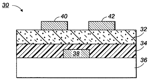
FIG. 2 schematically illustrates another TFT configuration 30 comprised of a
substrate 36, a gate electrode 38, a source electrode 40 and a drain electrode
42, an
insulating layer 34, and an organic semiconductor layer 32.
FIG. 3 schematically illustrates a further TFT configuration 50 comprised of a
heavily n-doped silicon wafer 56 which acts as both a substrate and a gate
electrode, a
thermally grown silicon oxide insulating layer 54, and an organic
semiconductor layer
52, on top of which are deposited a source electrode 60 and a drain electrode
62.
FIG. 4 schematically illustrates an additional TFT configuration 70 comprised
of substrate 76, a gate electrode 78, a source electrode 80, a drain electrode
82, an
organic semiconductor layer 72, and an insulating layer 74.
The substrate may be composed of for instance silicon, glass plate, plastic
film
or sheet. For structurally flexible devices, plastic substrate, such as for
example
polyester, polycarbonate, polyimide sheets and the like may be used. The
thickness of
the substrate may be from amount 10 micrometers to over 10 millimeters with an
exemplary thickness being from about 50 micrometers to about 2 millimeters,
especially for a flexible plastic substrate and from about 0.4 to about 10
millimeters
for a rigid substrate such as glass or silicon.
The gate electrode, the source electrode, and the drain electrode are
fabricated
by embodiments of the present invention. The thickness of the gate electrode
layer
ranges for example from about 10 to about 2000 nm. Typical thicknesses of
source
and drain electrodes are, for example, from about 40 nm to about 1 micrometer
with
the more specific thickness being about 60 to about 400 nm.
The insulating layer generally can be an inorganic material film or an organic
polymer film. Illustrative examples of inorganic materials suitable as the
insulating
layer include silicon oxide, silicon nitride, aluminum oxide, barium titanate,
barium
zirconium titanate and the like; illustrative examples of organic polymers for
the
insulating layer include polyesters, polycarbonates, poly(vinyl phenol),
polyimides,
polystyrene, poly(methacrylate)s, poly(acrylate)s, epoxy resin and the like.
The
thickness of the insulating layer is, for example from about 10 nm to about
500 nm
depending on the dielectric constant of the dielectric material used. An
exemplary
CA 02694777 2011-12-21
thickness of the insulating layer is from about 100 nm to about 500 nm. The
insulating layer may have a conductivity that is for example less than about
10-12
S/cm.
Situated, for example, between and in contact with the insulating layer and
the
source/drain electrodes is the semiconductor layer wherein the thickness of
the
semiconductor layer is generally, for example, about 10 nm to about 1
micrometer, or
about 40 to about 100 nm. Any semiconductor material may be used to form this
layer. Exemplary semiconductor materials include regioregular polythiophene,
oligthiophene, pentacene, and the semiconductor polymers disclosed in Beng Ong
et
al., US Patent Application Publication No. US 2003/0160230 A1; Beng Ong et
al., US
Patent Application Publication No. US 2003/0160234 Al; Beng Ong et al., US
Patent
Application Publication No. US 2003/0136958 Al; and "Organic Thin Film
Transistors for Large Area Electronics" by C. D. Dimitrakopoulos and P. R. L.
Malenfant, Adv. Mater., Vol. 12, No. 2, pp. 99-117 (2002). Any suitable
technique
may be used to form the semiconductor layer. One such method is to apply a
vacuum
of about 10-5 to 1 0-7 torr to a chamber containing a substrate and a source
vessel that
holds the compound in powdered form. Heat the vessel until the compound
sublimes
onto the substrate. The semiconductor layer can also generally be fabricated
by
solution processes such as spin coating, casting, screen printing, stamping,
or jet
printing of a solution or dispersion of the semiconductor.
The insulating layer, the gate electrode, the semiconductor layer, the source
electrode, and the drain electrode are formed in any sequence, particularly
where in
embodiments the gate electrode and the semiconductor layer both contact the
insulating layer, and the source electrode and the drain electrode both
contact the
semiconductor layer. The phrase "in any sequence" includes sequential and
simultaneous formation. For example, the source electrode and the drain
electrode
can be formed simultaneously or sequentially. The composition, fabrication,
and
operation of thin film transistors are described in Bao et al., US Patent
6,107,117.
16
CA 02694777 2010-02-26
=
The invention will now be described in detail with respect to specific
representative embodiments thereof, it being understood that these examples
are
intended to be illustrative only and the invention is not intended to be
limited to the
materials, conditions, or process parameters recited herein. All percentages
and parts
are by weight unless otherwise indicated. The phrases "room temperature" and
"ambient temperature" refer to a temperature range of about 20 to about 25
degrees C.
Unless otherwise indicated, "silver" nanoparticles refer to nanoparticles
having
elemental silver (that is, not a silver composite). For those Examples
involving a
plasma treatment, Harrick Plasma generator (PDC-32G) was used for the plasma
treatment. This generator has an input power of 100W.
Comparative Example 1
Silver nanoparticles stabilized with hexadecylamine were used, which were
aged for 3 months. 15 wt% solution of the nanoparticles in toluene was
prepared and
spin coated on a glass slide. After annealing at 140 C for 3 min,
conductivity of the
resulted film was measured using 4-probe method to be 1.7 X10⁻¹ S/cm.
Example 1
The above low conductivity thin film was immersed in 0.1 M acetic acid
solution in toluene for 5 min. After rinsing with toluene, the film was dried
at 140 C
for 1 min, resulting in a highly conductive film with a conductivity of 2.84
X104
S/cm. The conductivity was improved by 5 orders of magnitude.
Example 2
Similar to Example 1, the low conductivity thin film was immersed in 0.02 M
dilute acetic acid solution in toluene for 5 min. After rinsing with toluene,
the film
was dried at 140 C for 1 min, giving a highly conductive thin film with
conductivity
of 2.21 X10⁴ S/cm. The conductivity was improved by 5 orders of magnitude,
even
with a very dilution acid solution.
Comparative Example 2
Fresh silver nanoparticles stabilized with hexadecylamine were used. 15 wt%
solution of the nanoparticles in toluene was prepared and spin coated on glass
slides.
17
CA 02694777 2011-12-21
After annealing at 140 C for 10, a high conductivity of 2.1X10⁴ S/cm was
observed.
However, when annealed at 120 C for 10 min, conductivity was detected to be
4.8X10⁻² S/cm.
Example 3
This low conductivity thin film in Comparative Example 2 was immersed in
0.5 M acetic acid solution in toluene for 5 min. After rinsing with toluene,
the film
was dried at 120 C for 1 min, giving a highly conductive thin film with
conductivity
of 2.4 X 10⁴ S/cm, an improvement of 5-6 orders of magnitude. It also
indicates that
lower heating temperature can be used with the acid treatment process.
Example 4
The aged silver nanoparticles were formulated as ink by dispersing the
nanoparticles in a mixed solvent of dodecane and terpineol at 2:1 ratio. The
silver
nanoparticles loading was 40 wt%. Using inkjet printer, fine lines were jetted
on glass
substrate. The printed features were annealed at 120 C for 10 min, followed
by
treatment with 0.02 M acetic acid solution in toluene for 5 min. Highly
conductivity
lines were obtained by using two-probe measurement. The acid treatment step
had no
damage to the printed fine lines.
Example 5
Aged silver nanoparticles (3 weeks) were used. 15 wt% solution of the
nanoparticles in toluene was prepared and spin coated on glass slides. After
annealing
at 140 C for 3 min, conductivity of the resulted film was measured using 4-
probe
method to be ¨5.7 X 101 S/cm, which is about 5 orders of magnitude lower than
that
of fresh sample (-2 X10⁴ S/cm).
The low conductivity thin films were subjected to air plasma at room
temperature for different time from 10 to 120 seconds as shown in the
following table,
and the conductivity was measured with 4-probe method again. The following
table
summarizes the values. As one can see, the conductivity was improved to the
level of
fresh sample (-2 X 10⁴ S/cm) with plasma treatment for less than 30 seconds.
Longer
treatment to 120 seconds had no adverse effect on conductivity.
18
CA 02694777 2010-02-26
4 i
Time (s) 0 10 20 30 60
120
Conductivity 5.7X 10⁻¹ 1.27X104 = 1.52X10⁴ 2.01 X10⁴ 2.75X10⁴
2.80X10⁴
(S/cm2)
Example 6
Similar to Example 5, the film was annealed at 120 C for 10 min, followed by
air plasma treatment for 1 min at room temperature. The resulted film showed
conductivity as high as 2.45 X10⁴ S/cm.
Example 7
Similar to Example 4, the printed features were annealing at 120 C for 10
min, followed by air plasma treatment for 1 min. Highly conductivity lines
were
obtained by using two-probe measurement.
Example 8
Aged silver nanoparticles were used. 15 wt% solution of the nanoparticles in
toluene was prepared and spin coated on glass slides. The spin coating film
was
subject to air plasma for 1 min at room temperature. Conductivity of the
plasma
treated film was measured to be 8.4 X 10⁻³ S/cm. After the treatment, the film
was
annealed at 140 C for 3 min. The resulted film showed conductivity as high as
1.8
X104 S/cm. This revealed that plasma treatment prior to heating could also
effectively
improve the conductivity.
Example 9
Similar to Example 5, the low conductive films were subject to nitrogen or
argon plasma for 1 min at room temperature. Both films showed high
conductivity
over 104 S/cm.
Comparative Example 3
Similar to Example 6, silver nanoparticle thin-film was annealed at 120 C for
min, followed by irradiation with UV light for 7 min. (UV treatment is known
as a
surface cleaning method.) The resulted film showed very low conductivity which
is
19
CA 02694777 2010-02-26
=
the same as that before treatment, indicating that UV treatment has no
improvement
on conductivity of the film.
It will be appreciated that various of the above-disclosed and other features
and functions, or alternatives thereof, may be desirably combined into many
other
different systems or applications. Various presently unforeseen or
unanticipated
alternatives, modifications, variations or improvements therein may be
subsequently
made by those skilled in the art which are also intended to be encompassed by
the
following claims. Unless specifically recited in a claim, steps or components
of
claims should not be implied or imported from the specification or any other
claims as
to any particular order, number, position, size, shape, angle, color, or
material.