Note: Descriptions are shown in the official language in which they were submitted.
CA 02695003 2010-01-14
SYSTEM AND METHOD FOR ATTENUATION OF ELECTRICAL NOISE
FIELD OF THE PRESENT INVENTION
[0001] The Present Invention relates to electronic methods and systems for
the
high quality detection and monitoring of very weak signals. More particularly,
the
Present Invention relates to a signal conditioning method and apparatus for
suppressing or attenuating electrical noise while maintaining the strength and
integrity of the input signal coming from the object being detected and
viewed.
BACKGROUND OF THE PRESENT INVENTION
[0002] There are many currently-known electrical products generally
designed to
detect or monitor a weak signal, whether the signal is visual or optical,
magnetic,
auditory, pressure-based or any other sensory measurement. These products
include, for example, night vision binoculars, camera systems designed to
detect
images in sub-optimal conditions and listening devices designed to detect weak
or
distant sounds. In each of these products (along with similar-use products),
the
quality of the final or target image depends not only upon the strength and
quality of
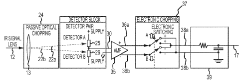
the signal coming from the target or object being detected, but also the
ability to
minimize the random "noise" generated in the electronics of the monitoring
device.
In an optical system, for example, this noise may be "dark current noise,"
which
includes what is referred to as 1/f noise, thermal noise from the
photodetector and
the preamplifier (known as "Johnson noise") and noise caused when voltage is
applied to the photodetector (known as "shot noise"). The greater the random
noise
inside a product is compared to the strength of the target signal, the poorer
the
quality of the final target image. If the internal noise is significant
compared to the
target signal, whether it is because the magnitude of the noise is so great or
the
strength of the target signal is very weak, it will detract from or blur the
image within
the system. And if the signal is weak and there is a lot of noise in the
system, the
final image can be completely hidden or obliterated.
[0003] The ratio of signal strength to the strength of electronic noise is
referred to
as the "signal-to-noise" ratio: The stronger the signal, the lower the noise;
or, the
1
CA 02695003 2010-01-14
,
higher the signal-to-noise ratio, the better is the quality of the image being
shown.
Currently-known products require that an input signal (e.g., light, magnetic
field,
vibration, sound, heat, pressure, etc.) being sensed by an appropriate
detector must
have a signal strength greater than the electrical noise (primarily coming
from the
detector and preamplifier in the system) of the input stage before it can be
reliably
detected and viewed. This means that the signal-to-noise ratio must be greater
than
1.0 before sensing is possible.
[0004] There exists several currently-known ways, or techniques, to
improve the
signal-to-noise ratio in an effort to keep it greater than 1Ø These
techniques
include: (1) amplifying the input signal and (2) filtering out the noise. Both
of these
techniques, however, require knowledge of the input signal in advance, or some
way
to identify the signal. That is, with regard to the former technique, the
input signal
must be known or identifiable in order to amplify it without amplifying the
electronic
noise that surrounds it, and with regard to the latter, the input signal must
also be
known in order to distinguish it from the noise that is being blocked by the
filter.
[0005] Currently-known methods for identifying an input or target
signal include:
(a) knowing the type of signal in advance; (b) having control over the input
signal and
coding it when it is transmitted, such as with signal modulation schemes; or
(c) time-
averaging techniques to detect repeating signals and distinguish them from non-
repeating random noise. Obviously, if the signal to be detected is not known
or
controlled in advance, none of the above techniques, other than time-
averaging, can
be used.
[0006] However, even if used, time-averaging techniques are limited
and
impractical because time-averaging, in general, is a relatively slow process
requiring
many samples to effectively reduce the noise that exists. Finally, none of the
currently-known techniques, including time-averaging, are effective for
detecting
short duration or transient images where there is insufficient data to analyze
the
signal.
[0007] The Present Invention overcomes the aforementioned
shortcomings of
the currently-known techniques, and provides drastically improved signal-to-
noise
ratios even in those situations where creation of the input signal is not
controlled,
2
CA 02695003 2013-05-14
93663-6
where the input signal is not known, and in situations where the target signal
is very
weak compared to a strong background signal. In particular, the Present
Invention
allows one to place "tags," or codes, on the input signal, when the input or
target signal
is not known in advance and no control over transmission of the target signal
is
available, such that background signals and noise can be effectively
attenuated and
filtered, while maintaining the integrity of the target signal. This provides
a high signal-
to-noise ratio and the detection of signals in a manner and having a quality
that has
heretofore never been obtainable.
SUMMARY OF THE PRESENT INVENTION
[0008] In one aspect of the invention, there is provided a method of
improving
signal-to-noise ratio, the method comprising: receiving an input image signal
through a
lens; splitting the input signal after exiting said lens into two components;
and applying a
reverse polarity on each split input signal component; superimposing the two
reverse
polarity input signal components into a superimposed signal; amplifying the
superimposed signal; receiving and reverse chopping the superimposed signal,
providing normal and inverted amplification signals; and superimposing the
normal and
inverted amplification signals into a restored signal.
[0009] In another aspect, there is provided a system for attenuating
electrical
noise, the system comprising: a lens; an input device for receiving an input
image signal
after passing through said lens; a first chopping device for splitting said
received input
signal into two separate time-phased input signals; two detectors of opposite
polarity,
each detector receiving one of said two separate time-phased input signals and
providing an electric current output signal; a first superimposing device to
superimpose
the two electric current output signals and forming a single detected signal;
a
preamplifier, having at least two inputs and an output, with the preamplifier
inputs
receiving a reference signal and the single detected signal; a second chopping
device,
synchronized to said first chopping device, for providing normal and inverted
amplification signals; and a second superimposing device to superimpose said
normal
and inverted amplification signals and provide a superimposed and restored
input
signal.
3
CA 02695003 2013-05-14
93663-6
[0010] In a further aspect, there is provided a system for
attenuating electrical
noise, the system comprising: a lens; an input device for receiving an input
image signal
after passing through said lens; a chopping device splitting said received
signal into two
separate input signals; two detectors of opposite polarity, each detector
receiving one of
said two separate input signals; and an output to each of said two detectors,
each
output of each detector joined and having only a single sense node between the
two
detector outputs, establishing a single dual detector output signal.
[0011] The Present Invention generally provides a method and system
to
attenuate electrical noise and background in a monitoring or detecting
product, thereby
being able to clearly reproduce and illustrate weak target input signals.
Background
signals in embodiments of the Present Invention are suppressed by what is
referred to
as "common mode rejection" techniques, that is, by techniques that cancel
common
mode signals and, here, that cancel common background noise. This noise
attenuation
is accomplished in the detector and preamplifier stage of a detector system,
where
significant noise is typically generated. Noise attenuation in embodiments of
the
Present Invention can be accomplished, and can provide enhanced images, where
the
target input signal is unknown, is of a transient nature or where there is
very little data
available to analyze the signal.
[0012] Following the teaching of the Present Invention, the target
input signal
(which can be any type of input, such as an optical signal or one of
vibration, magnetic
field, sound, heat, pressure, etc.) is split into two components, preferably
through a
process called "dither chopping" Each of the two components is then coded, or
"tagged," with a unique marker as the input signal components are converted
into an
electrical format. The unique encoding technique of the Present Invention
maintains full
view of the input scene and does not have scene blindness problems caused by
physical light shutters used in lock-in and synchronous detection systems. As
a
consequence, the noise reduction technology in the detection circuit of
embodiments of
the Present Invention do not suffer from a 50% loss in input signal strength
occurring in
current "chopper" based systems (e.g., having a physical input shutter), and,
therefore,
have up to twice the detection sensitivity. Significantly, the random noise,
containing
4
CA 02695003 2013-05-14
93663-6
white noise and non-white noise, generated in the system electronics in
embodiments of
the Present Invention is suppressed by lowering the non-white noise with
synchronous
phase detection and lowering the white noise by enabling reduced bandwidth in
operation. In an
4a
CA 02695003 2010-01-14
,
,
optical system using the Present Invention, for example, background signals
are
immediately suppressed at the detector by common mode rejection and the
detector
system "tagging" each input component with +1 or -1 polarity flags as the
signal
enters the optical-to-electrical conversion process. The tagged signal
components
are then synchronized with a second stage of reverse electronic chopping and
combined, thereby reestablishing and preserving the original input signal. In
this
reverse chopping stage, non-white random noise segments are cancelled and the
overall electrical noise effectively attenuated. The simultaneous combination
of full-
signal non-white noise suppression by polarity coding, common mode rejection
at
the sense node and white noise reduction by narrow bandwidth has never been
taught before. The preservation of the original input signal, while
attenuating
electronic noise, provides an exceptionally clear, relatively noise-free,
visual image.
[0013] Embodiments of the Present Invention thus include an input
signal
chopping device to produce at least two input signal components, and at least
two
detectors or an alternating detector system with opposite polarities to detect
the at
least two dither chopped input signal components while simultaneously
cancelling
background signals common to the detectors. Differential signals from the at
least
two detectors or alternating detector system are then superimposed to create a
single detector current signal. A preamplifier is provided to receive that
single
detector signal, followed by electronic switch means to flip polarity of
detected
current signal segments, thereby combining and reestablishing the original
input. A
low pass filter, an amplifier, and an analog-to-digital converter can also be
added,
resulting in a final digital detection signal.
BRIEF DESCRIPTION OF THE FIGURES
[0014] Features, aspects, and embodiments of the Present Invention
are
described in conjunction with the attached drawings, in which:
[0015] Figure 1 is a diagram illustrating an exemplary prior art
device, without the
detection system of the Present Invention;
[0016] Figure 2A is a diagram illustrating a portion of an optical
embodiment of
the Present Invention;
CA 02695003 2010-01-14
,
[0017] Figure 2B is a diagram illustrating an alternative
photovoltaic arrangement
for the sensors and amplifier shown in Figure 2A;
[0018] Figure 3 is another diagram illustrating further portions of
the optical
embodiment of the Present Invention;
[0019] Figure 4 is a diagram showing a portion of the signal
created after the
detectors and before the second electronic chopping stage in one embodiment of
the
Present Invention;
[0020] Figure 5 is a schematic representation of the optical
embodiment of the
Present Invention showing the original input signal and the resulting
electrical
components of that signal after the first chopping stage has been completed;
and
[0021] Figure 6 is a schematic representation of a low pass filter
and restored
input signal from one embodiment of the Present Invention.
DETAILED DESCRIPTION OF THE PREFERRED EMBODIMENTS
[0022] While the Present Invention is susceptible of embodiments in
many
different forms, there is shown in the, drawings and will herein be described
in detail,
preferred embodiments of the Present Invention with the understanding that the
present disclosure is to be considered as an exemplification of the principles
of the
Present Invention, and is not intended to limit the broad aspects of the
Present
Invention to the embodiments illustrated herein.
[0023] FIG. 1 is a diagram illustrating an exemplary optical
detection device, as it
may exist in the prior art. The image being detected is shown at 11, and the
input
signal from image 11 is represented by line 12. The input signal in this
example is
an optical signal and is received by optical lens 13. After exiting the lens,
the input
signal enters detector 14, exits detector 14 as electric analog detector
signal 15, and
enters preamplifier 16. Amplified signal 17 exits preamplifier 16 and enters
amplifier
18, where the input signal is amplified again. Signal 19 exiting amplifier 18
then
enters analog-to-digital converter 20, and exits as digital detected signal
21. Digital
detected signal 21 is then processed in any of the methods well-known in the
art.
6
CA 02695003 2010-01-14
[0024] The electronic noise that is addressed by the Present Invention is
created
at and between detector 14 and preamplifier 16, when the input signal is
converted
into an electrical form. Accordingly, the system of the Present Invention
replaces the
detector and preamplifier configuration of the currently-known devices. More
specifically, the components within the box labeled 10 in FIG 1 are replaced
by
components forming part of the Present Invention.
[0025] FIGS. 2A and 2B illustrate components of embodiments of the Present
Invention in which there is shown an optical system, such as could be used for
night
vision binoculars or a low light camera. It is recognized, however, that the
Present
Invention can also be used for other systems, such as those based upon
vibration,
sound, heat, pressure or the like.
[0026] In FIGS. 2A and 3, which illustrate different details and
representations of
the Present Invention, the image being detected is again shown at 11, as in
FIG. 1,
with an input signal shown at 12, and an optical lens shown at 13. There is
then
provided a method for splitting or dither chopping the input signal into two
separate
signals directed to two separate detectors. As shown in FIG. 2A, a method for
dither
chopping the input signal is accomplished by a physical beam steering system
(alternatively, any beam shift solution may be used to achieve the same end).
In
particular, the input signal exiting the lens is split into two separate time
division
multiplexed components, 22a and 22b, by a micromirror array, a single mirror
of
which is portrayed at 24 (see FIG. 5). In one embodiment of the Present
Invention
the micromirror array is a magnetic chopper steering mirror such as from
Sutech
Optical Model SF800M (see, www.sutechoptical.com). In another embodiment, the
micromirror array is a fast steering mirror such as from Newport (see,
www.newport.com/Fast-Steering-Mirrors/144996/1033/catalog.aspx).
[0027] The separate time division multiplexed components 22a and 22b are
then
directed to and enter two detectors 25 and 26. In Fig. 2A the two detectors
are
shown in a serial arrangement, having a bias on the detectors. Fig. 2B shows
an
alternative arrangement of the detectors 25 and 26, shown in a parallel
configuration
without any bias.. Alternatively, for a single point source, one can have a
single
signal with a modulating dual detector block, or for a larger image, a
microlens array
7
CA 02695003 2010-01-14
,
focusing the image and a modulating dual detector block, also dither chopping
the
signal. Additionally, dither chopping of the input signal may be accomplished
by
other means, including those that do not have moving parts. An example may be
the
use of refractive index steering (birefringent properties) as taught in
telecommunications applications.
[0028] Detectors 25, 26 shown in Fig. 2A have inverse polarities, such
that
opposite outputs are provided from each detector 25, 26 at any single point in
time.
That is, a positive polarity output will exist at one detector when a negative
polarity
output exists at the other detector. Such opposite polarities may be
established by
the position of the detector in the circuit, or by the inherent properties of
the detector.
For example, when using a resistive type detector (e.g., a thermistor, a
sensor that
changes resistance with changes in temperature), the polarity of the sensor is
established by its position in relation to the power supply. The orientation
of the
sensors in use is not significant. When using a polarity sensitive detector
(e.g., a
PZT or electret microphone, having a fixed internal voltage and polarity), on
the other
hand, the polarity is established by the internal voltage of the sensor. When
a
polarity sensitive detector is used, it must be connected to the appropriate
polarity of
the power supply. The complementary power supply voltages are then set to
produce a null at the junction of the voltage divider at sense node 27. This
configuration effectively "tags" each multiplexed input signal component with
a +1 or
-1 polarity, depending on the detector that is sensing the signal.
[0029] The Present Invention is not dependent on the specific type of
detectors
that are used. Detectors can range from visible to longwave infrared
detectors,
visible light detectors such as UDT Sensors CD-1705 silicon PiN photodectors,
to
long wave infrared detectors such as from Infrared Associates, Inc., Type MCT-
13
HgCdTe LWIR. Other detector families, including InGaAs and InSb detectors, can
also be used.
[0030] As shown in FIGS. 2A or 2B and 3, detector 25, at the designated
point in
time, is shown as providing a positive signal, and detector 26 is shown as
providing a
negative signal. A sense node 27 provides a single combined output of the
multiple
detectors. Thus, after the input signal is split and each multiplexed
component is
8
CA 02695003 2010-01-14
,
directed to detector 25 or 26, as referenced above, each component will be
tagged
with a positive or negative polarity. For example, with an optical detector
pair, a
positive signal is provided when detector 25 senses one component of the
multiplexed input light signal and a negative signal is provided when detector
26
senses the next time phased component of the input light signal. By having
only a
single sense node for the detector pair, any background light that is detected
by both
detectors at the same time will cancel each other out and result in a signal
of zero
background value.
[0031] An extremely fast and efficient dual optical detection circuit
based upon a
balanced, inverted parallel photodiode pair, known as an "opsistor," is shown
and
described in Chow et al., U. S. Patent No. 5,838,995, entitled "Wavelength-
Controllable Voltage-Phase Photodiode Optoelectronic Switch ," which is
incorporated herein by reference. The opsistor, photodiode pair is based upon
a
photovoltaic arrangement. A photoconductive arrangement with bias can also be
used, as is well known in the art.
[0032] FIG. 5 illustrates the physical chopping procedure and the
electrical
"tagged" signal that results after exiting the detector pair. The optical
input signal is
shown at 12. The physical mirror chopping, as described above, is
schematically
represented at 14. The two chopped components resulting from electronic
tagging
are graphically portrayed, with signal 30a representing the tagged positive
signal
from detector 25 (not illustrated), and signal 30b representing the tagged
negative
signal from detector 26 (not illustrated).
[0033] The resulting signal 30 from the detector pair shown in FIGS. 2
and 3 is
the superimposition of tagged signals 30a, 30b, as shown in FIG. 4, plus any
noise
that is created in the detector and amplifier as the input signal is converted
to an
electrical signal. As is seen, and a part of the innovation of the Present
Invention,
the dual detector arrangement provides two paths for injecting the input
signal into a
detection circuit, but only one noise waveform with which to contend. In other
words,
the physical chopping and tagging that is performed is only performed on the
input
signal, and any noise, which is added on signal 30, is not chopped or tagged.
This
will allow for identification of the tagged signal and filtered attenuation of
the
9
CA 02695003 2010-01-14
,
untagged noise.
[0034] As further shown in FIGS. 2 and 3, the resulting electrical
signal 30 is
amplified in amplifier 35, with balanced output, as is well known in the art.
Exiting
amplifier 35 are balanced outputs 36a, 36b. These outputs enter switching
network
37, which provides a second, electrical chopping or "reverse" chopping
process.
This second chopping process is synchronized to the first dithering chopping
frequency, whereby the dithered positive signals are passed and the dithered
negative signals are inverted. That is, there is a fundamental two-step
sequence.
First, the input signal is coded with a +1 and -1 polarity factor as it enters
the
electrical domain consisting of the detector and preamplifier circuit. Second,
inside
the electrical domain, a second stage of electronic chopping with +1 and -1
multipliers is synchronously phase-locked in the input signal dither chopping.
The
optimum frequency of the system chopping rates (e.g., of the chopping rates of
both
chopping steps), can be varied, but must be greater than the expected target
signal
bandwidth (e.g., the rate that the target signal is expected to change). A
preferred
chopping rate is approximately Ten (10) times the maximum expected target
signal
bandwidth (i.e., a detector system with 30 frame/sec response will use a
chopping
rate around 300 Hz). In this manner, much of the quasi-DC noise on the signal,
which was not chopped, will cancel itself out when passing through the
switching
network while white noise is attenuated by reduced bandwidth. The reverse
chopped signals exiting this second electronic chopping circuit are shown at
38a and
38b.
[0035] Reverse chopped signals 38a, 38b enter low pass filter 39, as
illustrated
in FIG. 6. Low pass filter 39 passes the low frequency input signal and
filters out any
remaining high frequency noise. Exiting low pass filter 39 is the final
restored input
signal, also shown in FIG. 6, which corresponds to a relatively noise-free
signal 17
that can be input to amplifier 18 and analog-to-digital converter 20, as shown
in the
remaining system illustrated in FIG. 1.
[0036] The disclosed Present Invention provides a system and method
for
attenuating electrical noise. It should be noted that the above-described and
CA 02695003 2010-01-14
,
illustrated embodiments and preferred embodiments of the Present Invention are
not
an exhaustive listing of the form the Present Invention might take; rather,
they serve
as exemplary and illustrative of embodiments of the Present Invention as
presently
understood. Many other forms of the Present Invention exist and are readily
apparent to one having ordinary skill in the art.
11