Note: Descriptions are shown in the official language in which they were submitted.
CA 02695853 2010-02-04
WO 2009/021069 PCT/US2008/072379
ELECTRICALLY AND THERMALLY NON-METALLIC
CONDUCTIVE NANOSTRUCTURE-BASED ADAPTERS
TECHNICAL FIELD
[0001] The present invention relates to electrical and thermal adapters, and
more particularly, to nanostructure-based adapters designed to maximize
interaction between a nanoscale conductive element and a traditional
electrical
and/or thermal circuit system.
BACKGROUND ART
[0002] The joining of electrical conductors to another element, such as a
connector, in a system usually involves the use of an adhesive, and/or the use
of
mechanical means, such as crimping or a solder connection. All of these have
some disadvantages.
Adhesives
[0003] Electrical or thermal contact between elements can sometimes be
provided by means of an adhesive. For example, a joint between a high surface
area element in an electrolytic capacitor may be formed by means of a complex
cellulose binder and an aluminum or titanium foil. This type of binding system
can generate a substantially high internal resistance that can severely
degrade
the performance of the capacitor. This internal resistance can also serve to
increase the capacitor time constant (i=R*C). Other binding examples can
include epoxy bonding of the components involved. Such bonding may have
dual functions, including (1) providing a mechanical bond, and (2) carrying
heat, as seen with bonding of elements of an airplane or jet engine close to a
heat source.
[0004] In the case of thermal junctions, the provision of good contact area
can
often be difficult. For example, it can be difficult to provide a good contact
at
the junction between an integrated circuit housing and a heat sink, where a
thermal resistance of more than 20 degrees may be needed to drive, for
instance,
150 watts per square cm though the junction.
1
CA 02695853 2010-02-04
WO 2009/021069 PCT/US2008/072379
Mechanical Means
[0005] It has been shown by the Kuhlmann-Wilsdorf theory of electrical
contacts, and by analogy through the R.Holm theory for electrical contacts,
that
electrical current or thermal energy must necessarily pass though two
contacting
surfaces in only a few, or perhaps up to 50 atomic contact spots.
Interestingly,
this is not strongly dependent on the total area of contact, but rather can be
dependent upon clamping force between contacts. This limitation of the total
surface area that may be in actual contact between a connector and its
corresponding contacting element can generally introduce a severe electrical
or
thermal contact resistance.
Solder Connections
[0006] To overcome this contact resistance and improve overall conductivity,
the effective contact area may need to be increased. One means of
accomplishing this is by soldering. However, the lead-tin alloys in common use
for soldering, or even lead free solders (e.g., silver-antimony-tin), can have
a
strong tendency to form intermetallic compounds or layers at the solder j oint
or
junction. Formation of intermetallic compounds usually occurs because, for
instance, the tin-copper etc., present in the solder can exhibit fast
diffusion
when coupled with common conductors, such as copper, generally used for both
thermal and electrical conduction. Moreover, the formation of intermetallic
compounds or layers can continue to occur, over time, even at ambient
temperatures. The consequence of such a formation at these junctions is that
the
intermetallic layer itself can become brittle (i.e., degradable), as well as
electrically and thermally resistive, leading to an increasing resistance or
even a
catastrophic mechanical failure at solder junctions, especially when these
junctions have a different coefficient of thermal expansion.
[0007] This holds true for both thermal and electrical junctions. Examples of
solder system degradation due to intermetallic formations have been widely
reported in the automotive industry, aerospace industry, and even in military
missiles.
2
CA 02695853 2010-02-04
WO 2009/021069 PCT/US2008/072379
[0008] A common approach for addressing this problem has been the
introduction of a "silver powder containing grease" between a heat generating
element and a heat dissipating element. This grease can increase thermal
transport, as it provides an additional thermal path, even though the grease
may
be of high thermal resistance itself. Fillers, such as silver powders, can
often be
added to this grease, and can also help in improving heat.
[0009] In addition to the above issues, there does not currently exist a
design for
joining and maximizing the number of conductive nanostructures involved in
conductivity to the devices in the macro-world, while enhancing or maintaining
the efficiency of the electrical or thermal transport exhibit by these
conductive
nanostructures.
[00010] In light of these issues, it would be desirable to provide a way to
allow
for efficient interaction between a nanoscale conductive element and the
traditional electrical and/or thermal circuit system, while minimizing
electrical
or thermal resistance and improve overall conductivity.
SUMMARY OF THE INVENTION
[00011] The present invention provides, in accordance with one embodiment, a
conductive adapter. The adapter includes, in an embodiment, a conducting
member made from a conductive nanostructure-based material and having
opposing ends. Such a material may be wires, yarns, tapes, ribbons or sheets
made from carbon nanotubes. In an embodiment, the conducting member can
be made from one of carbon, copper, silver, boron, boron-nitride, MoSz or
similar compounds, or a combination thereof. The adapter can also include a
connector portion positioned on one end of the conducting member for
maximizing a number of conductive nanostructures within the conducting
member in contact with connector portion, so as to enable efficient conduction
between a nanoscale environment and a traditional electrical and/or thermal
circuit system. In one embodiment, the connector portion may be made from
one of copper, aluminum, gold, silver, silver coated copper, cadmium, nickel,
tin, bismuth, arsenic, alloys of these metals, boron, boron nitride, glassy
carbon,
3
CA 02695853 2010-02-04
WO 2009/021069 PCT/US2008/072379
ceramics, silicon, silicon compounds, gallium arsenic, a combination thereof,
or
other materials capable of being electrically and/or thermally conductive. The
adapter may further include a coupling mechanism situated between the
conducting member and the connector portion, to provide a substantially
uniform contact between the conductive nanostructure-based material in the
conducting member and the connector portion. In one embodiment, the coupling
mechanism may be a glassy carbon material capable of providing substantially
low resistance coupling. The coupling mechanism may also provide the
conducting member with substantially uniform contact to the connector portion
across a contact surface area on the connector portion.
[00012] In an alternate embodiment, the connector portion may be deposited,
such as by electroplating, on at least on of the opposing ends of the
conducting
member. In this embodiment, connector portion can be made from one of gold,
silver, nickel, aluminum, copper, bismuth, tin, zinc, cadmium, tin-nickel
alloy,
copper alloy, tin-zinc alloy, bismuth-copper alloy, cadmium-nickel alloy,
other
conductive metals and their alloys, or a combination thereof. Moreover, the
conducting member can be imparted with a design to permit extension of the
conducting member in at least one direction.
[00013] In another embodiment of the present invention, there is provided a
method for making a conductive adapter. The method includes initially
providing a conducting member made from a nanostructure-based material and
a connector portion to which the conducting member may be joined. The
conducting member, in one embodiment, can be wires, yarns, tapes, ribbons or
sheets made from nanotubes. The nanotubes can be made from one of carbon,
copper, silver, boron, boron-nitride, MoSz or similar compounds, or a
combination thereof. In one embodiment, the connector portion may be made
from one of copper, aluminum, gold, silver, silver coated copper, boron, boron
nitride, glassy carbon, ceramics, silicon, silicon compounds, gallium arsenic,
a
combination thereof, or other materials capable of being electrically and/or
thermally conductive. Next, a coupling mechanism may be placed at a junction
between the conducting member and the connector portion. In an embodiment,
the coupling mechanism may be a glassy carbon precursor, such as furfuryl
4
CA 02695853 2010-02-04
WO 2009/021069 PCT/US2008/072379
alcohol, Resol resin, or any material known to form glassy carbon when heat
treated that can be deposited into the junction. The conducting member and
connector portion may thereafter be held against one another, while the
junction
is heated to pyrolyze the glassy carbon precursor to form a glassy carbon low
resistance coupling mechanism. In one embodiment, the minimum temperature
of pyrolysis should be at least in the neighborhood of about 400 C or higher.
It
should be appreciated that material that may be sensitive to this temperature
may not be suitable for this invention. Moreover, pyrolysis need not go to
completion for this junction to offer substantially superior contact
resistance to
the traditional means for coupling conducting members.
[00014] In a further embodiment of the invention, there is provided another
method for making an conductive adapter. The method includes initially
providing a conducting member made from a nanostructure-based material and
having opposing ends. The conducting member, in one embodiment, can be
wires, yarns, tapes, ribbons or sheets made from nanotubes. The nanotubes can
be made from one of carbon, copper, silver, boron, boron-nitride, MoSz or
similar compounds, or a combination thereof. Next, a connector portion may be
deposited on at least one end of the conducting member for maximizing a
number of conductive nanostructures within the conducting member in contact
with connector portion, so as to enable efficient conduction between a
nanoscale
environment and a traditional electrical and/or thermal circuit system. In an
embodiment, deposition can be accomplished by electroplating the connector
portion on each of the opposing ends of the conducting member. In such an
embodiment, one of gold, silver, nickel, aluminum, copper, bismuth, tin, zinc,
cadmium, tin-nickel alloy, copper alloy, tin-zinc alloy, bismuth-copper alloy,
cadmium-nickel alloy, other conductive metals and their alloys, or a
combination thereof may be used to deposit the connector portion on each of
the
opposing ends of the conducting member. The method further including
providing a patterned conducting member to permit extension of the conducting
member in at least one direction. In particular, the design on the conducting
member may be such that it permits extension of the conducting member along
one of an X axis, Y axis, or a combination thereof.
CA 02695853 2010-02-04
WO 2009/021069 PCT/US2008/072379
BRIEF DESCRIPTION OF DRAWINGS
[00015] Figs. lA-B illustrate a Chemical Vapor Deposition system for
fabricating nanotubes, in accordance with one embodiment of the present
invention.
[00016] Fig. 2 illustrates an electrically and thermally conductive adapter in
accordance with one embodiment of the present invention.
[00017] Fig. 3 illustrates an electrically and thermally conductive adapter in
accordance with another embodiment of the present invention
[00018] Figs. 4A-E illustrate an extendible electrically and thermally
conductive
adapter in accordance with various embodiments of the present invention.
DESCRIPTION OF SPECIFIC EMBODIMENTS
[00019] The need to carry relatively high current pulses between two movable
conductors, such as a high energy capacitor, a ground strap, a bus bar or bus
pipe, or pulse generating circuit, to an external circuit without degradation
of
the waveform or without heating of a junction requires careful engineering of
the conduction path. This can be important where the conductor may be subject
to movement which might cause fatigue damage in more commonly used
copper conductors. To satisfy this need, the present invention provides, in an
embodiment, a an approach for carrying relatively high current pulses through
the use of a nanostructure-based conducting member, such as that made from
carbon nanotubes in the form of, for example, a ribbon, a spun cable, or a
sheet.
[00020] Presently, there exist multiple processes and variations thereof for
growing nanotubes, and forming sheets or cable structures made from these
nanotubes. These include: (1) Chemical Vapor Deposition (CVD), a common
process that can occur at near ambient or at high pressures, and at
temperatures
above about 400 C, (2) Arc Discharge, a high temperature process that can
give
rise to tubes having a high degree of perfection, and (3) Laser ablation.
6
CA 02695853 2010-02-04
WO 2009/021069 PCT/US2008/072379
[00021] The present invention, in one embodiment, employs a CVD process or
similar gas phase pyrolysis procedures known in the industry to generate the
appropriate nanostructures, including carbon nanotubes. Growth temperatures
for a CVD process can be comparatively low ranging, for instance, from about
400 C to about 1350 C. Carbon nanotubes, both single wall (SWNT) or
multiwall (MWNT), may be grown, in an embodiment of the present invention,
by exposing nanoscaled catalyst particles in the presence of reagent carbon-
containing gases (i.e., gaseous carbon source). In particular, the nanoscaled
catalyst particles may be introduced into the reagent carbon-containing gases,
either by addition of existing particles or by in situ synthesis of the
particles
from a metal-organic precursor, or even non-metallic catalysts. Although both
SWNT and MWNT may be grown, in certain instances, SWNT may be selected
due to their relatively higher growth rate and tendency to form rope-like
structures, which may offer advantages in handling, thermal conductivity,
electronic properties, and strength.
[00022] The strength of the individual carbon nanotubes generated in
connection
with the present invention may be about 30 GPa or more. Strength, as should
be noted, is sensitive to defects. However, the elastic modulus of the carbon
nanotubes fabricated in the present invention may not be sensitive to defects
and
can vary from about 1 to about 1.2 TPa. Moreover, the strain to failure of
these
nanotubes, which generally can be a structure sensitive parameter, may range
from a about 10% to a maximum of about 25% in the present invention.
[00023] Furthermore, the nanotubes of the present invention can be provided
with relatively small diameter. In an embodiment of the present invention, the
nanotubes fabricated in the present invention can be provided with a diameter
in
a range of from less than 1 nm to about 10 nm.
[00024] The nanotubes of the present invention can also be used as a
conducting
member to carry relatively high current similar to a Litz wire or cable.
However, unlike a Litz wire or cable soldered to a connector portion, the
nanotube conducting member of the present invention can exhibit relatively
lower impedance in comparison. In particular, it has been observed in the
7
CA 02695853 2010-02-04
WO 2009/021069 PCT/US2008/072379
present invention that the shorter the current pulses, the better the nanotube-
based wire cable or ribbon would perform when compared with a copper ribbon
or Litz wire. One reason for the observed better performance may be that the
effective frequency content of the pulse, which can be calculated from the
Fourier Transform of the waveform for current pulses that are square and
short,
e.g., about 100 ms to less than about 1 ms, can be very high. Specifically,
individual carbon nanotubes of the present invention can serve as conducting
pathways, and due to their small size, when bulk structures are made from
these
nanotubes, the bulk structures can contain extraordinarily large number of
conducting elements, for instance, on the order of 1014/cm2 or greater.
[00025] Carbon nanotubes of the present invention can also demonstrate
ballistic
conduction as a fundamental means of conductivity. Thus, materials made from
nanotubes of the present invention can represent a significant advance over
copper and other metallic conducting members under AC current conditions.
However, joining this type of conducting member to an external circuit
requires
that essentially each nanotube be electrically or thermally contacted to avoid
contact resistance at the junction.
[00026] It should be noted that although reference is made throughout the
application to nanotubes synthesized from carbon, other compound(s), such as
boron, MoSz, or a combination thereof may be used in the synthesis of
nanotubes in connection with the present invention. For instance, it should be
understood that boron nanotubes may also be grown, but with different
chemical precursors. In addition, it should be noted that boron may also be
used
to reduce resistivity in individual carbon nanotubes. Furthermore, other
methods, such as plasma CVD or the like can also be used to fabricate the
nanotubes of the present invention.
System for Fabricating Nanotubes
[00027] With reference now to Fig. 1A, there is illustrated a system 10,
similar to
that disclosed in U.S. Patent Application Serial No. 11/488,387 (incorporated
herein by reference), for use in the fabrication of nanotubes. System 10, in
an
embodiment, may be coupled to a synthesis chamber 11. The synthesis
8
CA 02695853 2010-02-04
WO 2009/021069 PCT/US2008/072379
chamber 11, in general, includes an entrance end 111, into which reaction
gases
(i.e., gaseous carbon source) may be supplied, a hot zone 112, where synthesis
of extended length nanotubes 113 may occur, and an exit end 114 from which
the products of the reaction, namely the nanotubes and exhaust gases, may exit
and be collected. The synthesis chamber 11, in an embodiment, may include a
quartz tube 115 extending through a furnace 116. The nanotubes generated by
system 10, on the other hand, may be individual single-walled nanotubes,
bundles of such nanotubes, and/or intertwined single-walled nanotubes (e.g.,
ropes of nanotubes).
[00028] System 10, in one embodiment of the present invention, may also
include a housing 12 designed to be substantially airtight, so as to minimize
the
release of potentially hazardous airborne particulates from within the
synthesis
chamber 11 into the environment. The housing 12 may also act to prevent
oxygen from entering into the system 10 and reaching the synthesis chamber 11.
In particular, the presence of oxygen within the synthesis chamber 11 can
affect
the integrity and compromise the production of the nanotubes 113.
[00029] System 10 may also include a moving belt 120, positioned within
housing 12, designed for collecting synthesized nanotubes 113 made from a
CVD process within synthesis chamber 11 of system 10. In particular, belt 120
may be used to permit nanotubes collected thereon to subsequently form a
substantially continuous extensible structure 121, for instance, a non-woven
sheet. Such a non-woven sheet may be generated from compacted, substantially
non-aligned, and intermingled nanotubes 113, bundles of nanotubes, or
intertwined nanotubes (e.g., ropes of nanotubes), with sufficient structural
integrity to be handled as a sheet.
[00030] To collect the fabricated nanotubes 113, belt 120 may be positioned
adjacent the exit end 114 of the synthesis chamber 11 to permit the nanotubes
to
be deposited on to belt 120. In one embodiment, belt 120 may be positioned
substantially parallel to the flow of gas from the exit end 114, as
illustrated in
Fig. lA. Alternatively, belt 120 may be positioned substantially perpendicular
to the flow of gas from the exit end 114 and may be porous in nature to allow
9
CA 02695853 2010-02-04
WO 2009/021069 PCT/US2008/072379
the flow of gas carrying the nanomaterials to pass therethrough. Belt 120 may
be designed as a continuous loop, similar to a conventional conveyor belt. To
that end, belt 120, in an embodiment, may be looped about opposing rotating
elements 122 (e.g., rollers) and may be driven by a mechanical device, such as
an electric motor. Alternatively, belt 120 may be a rigid cylinder. In one
embodiment, the motor may be controlled through the use of a control system,
such as a computer or microprocessor, so that tension and velocity can be
optimized.
[00031] In an alternate embodiment, instead of a non-woven sheet, the
fabricated
single-walled nanotubes 113 may be collected from synthesis chamber 11, and a
yarn 131 may thereafter be formed. Specifically, as the nanotubes 113 emerge
from the synthesis chamber 11, they may be collected into a bundle 132, fed
into intake end 133 of a spindle 134, and subsequently spun or twisted into
yarn
131 therewithin. It should be noted that a continual twist to the yarn 131 can
build up sufficient angular stress to cause rotation near a point where new
nanotubes 113 arrive at the spindle 134 to further the yarn formation process.
Moreover, a continual tension may be applied to the yarn 131 or its
advancement into collection chamber 13 may be permitted at a controlled rate,
so as to allow its uptake circumferentially about a spool 135.
[00032] Typically, the formation of the yarn 131 results from a bundling of
nanotubes 113 that may subsequently be tightly spun into a twisting yarn.
Alternatively, a main twist of the yarn 131 may be anchored at some point
within system 10 and the collected nanotubes 113 may be wound on to the
twisting yarn 131. Both of these growth modes can be implemented in
connection with the present invention.
Conductive Adapter
[00033] To carry relatively high current pulses between two movable
conductors,
such as a high energy capacitor, a ground strap, a bus bar or bus pipe, or
pulse
generating circuit, to an external circuit without degradation of the waveform
or
without heating of ajunction, the present invention provides, in an
embodiment,
a conductive adapter 20, such as that shown in Fig. 2. The conductive adapter
CA 02695853 2010-02-04
WO 2009/021069 PCT/US2008/072379
20 can include, among other things, a conductive nanostructure-based material
21, a connector portion 22, and a coupling mechanism 23 made from a material
capable of providing substantially low resistance coupling, while
substantially
maximizing the number of conductive nanostructures that can be actively
involved in conductivity.
[00034] In accordance with one embodiment, the adapter 20 includes a
conducting member 21 made from a conductive nanostructure-based material.
The conductive nanostructure-based material, in an embodiment, may be yarns,
ribbons, wires, cables, tapes or sheets (e.g., woven or non-woven sheets) made
from carbon nanotubes fabricated in a manner similar to that disclosed above
in
U.S. Patent Application No. 11/488,387. In an embodiment, conducting
member 21 may be made from one of carbon, copper, silver, boron-nitride,
boron, MoSz, or a combination thereof. Moreover, the material from which the
conducting member 21 may be made can include, in an embodiment, graphite of
any type, for example, such as that from pyrograph fibers.
[00035] The adapter 20 can also include a connector portion 22 to which the
conducting member 21 may be joined. In one embodiment, the connector
portion 22 may be made from a metallic material, such as copper, aluminum,
gold, silver, silver coated copper, cadmium, nickel, tin, bismuth, arsenic,
alloys
of these metals, boron, boron nitride, a combination thereof, or other
materials
capable of being electrically and/or thermally conductive. The connector
portion 22 may also be made from non-metallic material, such as those having
glassy carbons, ceramics, silicon, silicon compounds, gallium arsenide or
similar materials, or a combination thereof, so long as the material can be
electrically and/or thermally conductive. The connector portion 22, in and
embodiment, when coupled to conducting member 21, permits relatively high
current from a source that may be carried by the conducting member 21 to be
directed to an external circuit without substantial degradation.
[00036] To do so, the adapter 20 may further include a coupling mechanism 23
situated between the conducting member 21 and the connector portion 22, so as
to join the conducting member 21 to the connector portion 22. In one
11
CA 02695853 2010-02-04
WO 2009/021069 PCT/US2008/072379
embodiment, the coupling mechanism 23 may be made from a glassy carbon
material capable of providing substantially low resistance coupling. Glassy
carbon, in general, may be a form of carbon related to carbon nanotubes and
can
contain a significant amount of graphene like ribbons comprising a matrix of
amorphous carbon. These ribbons include sp2 bonded ribbons that can be
substantially similar to the sp2 bonded nanotubes. As a result, they can have
relatively good thermal and electrical conductivity. Examples of precursor
materials from which glassy carbon can be made include furfuryl alcohol,
RESOL resin (i.e., catalyzed alkyl-phenyl formaldehyde), PVA, or liquid resin
or any material known to form glassy carbon when heat treated. Of course,
other commercially available glassy carbon materials or precursor materials
can
be used.
[00037] In addition, coupling mechanism 23 may also provide the conducting
member 21 with substantially uniform contact to the connector portion 22
across a contact surface area on the connector portion 22. To that end, the
coupling mechanism 23 can act to substantially maximize the number of
conductive nanostructures within the conducting member 21 that can be actively
involved in conductivity to enhance efficiency of electrical and thermal
transport. For instance, relatively high current from a source and carried by
the
conducting member 21 can be directed to an external circuit without
substantial
degradation. The adapter 20 of the present invention, thus, can be used to
enable efficient conduction to a standard connector for use in a traditional
electrical and/or thermal circuit systems. In particular, adapter 20 can
enable
efficient interaction, for instance, through electrical and/or thermal
conduction,
between a nanoscale environment and the traditional electrical and/or thermal
circuit system.
[00038] For comparison purposes, the electrical and thermal conduction
properties for glassy carbon is compared to those properties exhibited by
graphite. As illustrated in Table 1 below, the presence of the graphene
ribbons
can enhance the electrical and therefore the thermal conductivity of glassy
carbon relative to that observed with graphite.
12
CA 02695853 2010-02-04
WO 2009/021069 PCT/US2008/072379
Table I
['aramctcr Grahhitc Glassy Carbon
Electrical resistivity 14.70 x 10 ohm-cm 0.50 x 10 ohm-cm
Thermal conductivity 95 w/ rri K 6.3 w/rri K
[00039] In another embodiment, there is provided a method for making a
conductive adapter of the present invention. The method includes initially
providing a conducting member, similar to conducting member 21, made from a
nanostructure-based material, and a connector portion, similar to connector
portion 22, to which the conducting member may be joined. The nanostructure-
based material, in one embodiment, can be those made from conductive carbon
nanotube, for instance, yarns, tapes, cables, ribbons, or sheets made from
carbon
nanotubes. The connector portion, on the other hand, may be made from a
metallic material, such as copper, nickel, aluminum, silver, gold, cadmium,
tin,
bismuth, arsenic, alloys of these metals, boron, boron-nitride, other
conductive
metals, any conductive metals coated with gold or silver, or a combination
thereof. The connector portion may also be made from non-metallic material,
such as those having glassy carbon forms, ceramics, silicon, silicon
compounds,
gallium arsenide, or similar materials, so long as the material can be
electrically
and/or thermally conductive.
[00040] Next, a coupling mechanism, similar to coupling mechanism 23, may be
placed at a junction between the conducting member and the connector portion.
In an embodiment, the coupling mechanism may be a glassy carbon precursor,
such as furfuryl alcohol, Resol resin, PVA or any material known to form
glassy
carbon when heat treated that can be deposited into the junction. It should be
appreciated that the tendency of the glassy carbon resin or material to "wet"
the
nanotubes in the conducting member can help to coat each individual nanotube,
so that each nanotube can contribute to electron or thermal transport.
[00041] The conducting member and connector portion may thereafter be held
against one another, while the junction between the conducting member and the
connector portion may be heated to a temperature range sufficient to pyrolyze
13
CA 02695853 2010-02-04
WO 2009/021069 PCT/US2008/072379
the glassy carbon precursor to form a glassy carbon low resistance coupling
mechanism. In one embodiment, the minimum temperature of pyrolysis should
be at least in the neighborhood of about 400 C to about 450 C. If pyrolysis
is
carried out in an inert atmosphere, the temperature may need to be higher to
permit the pyrolysis process to go to completion.
[00042] It should be appreciated that materials that may be sensitive to this
temperature may not be suitable for this invention. Moreover, pyrolysis need
not go to completion for this junction to offer substantially superior contact
resistance to the traditional means for coupling conducting members.
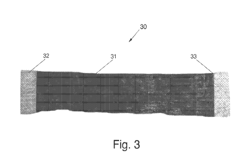
[00043] Looking now at Fig. 3, in accordance with another embodiment of the
present invention, there is shown a conductive adapter 30, for carrying
relatively high current from a source to an external circuit without
substantial
degradation of the waveform or without substantially heating of a junction.
[00044] In the embodiment shown in Fig. 3, adapter 30 includes a conducting
member 31 made from a conductive nanostructure-based material. The
conductive nanostructure-based material, in an embodiment, may include yarns,
ribbons, cables, tapes or sheets (e.g., woven or non-woven sheets) made from
carbon nanotubes fabricated in a manner similar to that disclosed above in
U.S.
Patent Application No. 11/488,387. In an embodiment, conducting member 31
may be made from one of carbon, copper, silver, boron-nitride, boron, MoSz, or
a combination thereof. The material from which the conducting member 31
may be made can also include, in an embodiment, graphite of any type, for
example, such as that from pyrograph fibers.
[00045] Adapter 30, as illustrated, can also include a connector portion 32 at
each of opposing ends of the conducting member 31. In one embodiment of the
invention, connector portion 32 may be a coating deposited, such as
electroplating, directly on each end of conducting member 31. Deposition or
electroplating of connector portion 32 on to conducting member 31 can be
carried out using methods well known in the art. Examples of electroplated
connector portion 32 include gold, silver, nickel, aluminum, copper, bismuth,
tin, zinc, cadmium, tin-nickel alloy, copper alloy, tin-zinc alloy, bismuth-
copper
14
CA 02695853 2010-02-04
WO 2009/021069 PCT/US2008/072379
alloy, cadmium-nickel alloy, other conductive metals and their alloys, or a
combination thereof.
[00046] Connector portion 32, in an embodiment, may be deposited or
electroplated on to conducting member 31 substantially uniformly, so as to
permit substantially uniform contact of the nanotubes in conducting member 31
across a contact surface area on the connector portion 32. As such, the
connector portion 32 can act to substantially maximize the number of
conductive nanostructures within the conducting member 31 that can be actively
involved in conductivity to enhance efficiency of electrical and thermal
transport and reduce contact resistance. To that end, relatively high current
from a source and carried by the conducting member 31 can be directed to an
external circuit without substantial degradation. The adapter 30, thus, can be
used to enable efficient interaction, for instance, through electrical and/or
thermal conduction, between a nanoscale environment and the traditional
electrical and/or thermal circuit system, as well as conduction to a standard
connector for use in a traditional electrical and/or thermal circuit systems.
[00047] With reference now to Figs. 4A-B, in accordance with a further
embodiment of the present invention, an adapter 40 can be designed to extend
or expand in at least one direction, for instance, lengthwise, without
compromising or substantially changing the resistivity of the adapter 40. In
other words, resistivity or the resistance property of the adapter 40 can be
independent of extension or expansion of adapter 40, even if the extension or
expansion is to a substantially extreme degree.
[00048] Adapter 40, in one embodiment, includes a conducting member 41 made
from a conductive nanostructure-based material. Such a material may be a
sheet (e.g., woven or non-woven sheet) a plurality of tapes or ribbons made
from carbon nanotubes, similar in manner to that disclosed in U.S. Patent
Application No. 11/488,387. Moreover, the material from which the conducting
member is made may include, in an embodiment, graphite of any type, for
example, such as that from pyrograph fibers.
CA 02695853 2010-02-04
WO 2009/021069 PCT/US2008/072379
[00049] However, unlike adapter 30 shown in Fig. 3, conducting member 41 of
adapter 40 may be imparted or etched with various patterns, including that
shown in Figs. 4A and 4B to permit the adapter 40 to extend or expand, for
instance, in a lengthwise direction (i.e., along the X axis) when pulled
axially
from opposite ends of the adapter 40 (see Fig. 4B). It should be appreciated
that
in addition to the patterns shown in Figs. 4A and 4B, the conducting member 41
may include other patterns or designs, so long as such a pattern or design
permits extension of adapter 40.
[00050] Although shown extending in a lengthwise direction, adapter 40 may
also be designed to extend along its width (i.e., along the Y axis). As shown
in
Figs. 4C-D, conducting member 41 may be provided with any pattern known in
the art that allows the adapter 40 to extend or be extensible along its width.
It
should be appreciated that conducting member 41 may also include a pattern
that allows the adapter 40 to extend lengthwise as well as along its width
(i.e., in
two dimensions).
[00051] To the extent desired, looking now at Fig. 4E, adapter 40 may include
two or more layers of conducting member 41, one on top of the other, and
substantially non-bonded to one another, along their length, so that adapter
40
may also be extendible along the Z axis. In such an embodiment, conducting
members 41 may be bonded to one another along their respective edges 43. In
an embodiment bonding of the edges 43 can be accomplished by the use of a
glassy carbon material, such as that provided above.
[00052] In addition to being extendible, conducting member 41 may also be
provided with shape memory capability. Specifically, the nanotubes from
which conducting member 41 may be made can permit the conducting member
41 to retract substantially back to its originally length, width or shape (see
Fig.
4A) after the conducting member 41 has been extended (see Fig. 4B) along
one, two or three dimensions.
[00053] The pattern, design or etching provided on conducting member 41, in an
embodiment, may be implement by processes known in the art, include
stamping, laser etching etc.
16
CA 02695853 2010-02-04
WO 2009/021069 PCT/US2008/072379
[00054] The adapter 40 can also include a connector portion 42 at each of
opposing ends of the conducting member 41. In one embodiment of the
invention, connector portion 42 may be a coating deposited, such as by
electroplating, directly on each end of conducting member 41. Deposition or
electroplating of connector portion 42 on to conducting member 41 can be
carried out using methods well known in the art. In one embodiment, the
connector portion 42 may be made from a metallic material, such as gold,
silver,
nickel, aluminum, copper, bismuth, tin, zinc, cadmium, tin-nickel alloy,
copper
alloy, tin-zinc alloy, bismuth-copper alloy, cadmium-nickel alloy, other
conductive metals and their alloys, or a combination thereof. The connector
portion 42 may also be made from non-metallic material, such as those having
glassy carbon forms, or similar materials, so long as the material can be
electrically and/or thermally conductive. To the extent that the adapter 40
may
be designed to allow conducting member 41 to extend or be extensible along its
width, similar to that shown in Fig. 4D, connector portion 42 may also be
designed to extend or be extensible widthwise along with the conducting
member 41.
[00055] In accordance with one embodiment, connector portion 42 may be
deposited or electroplated on to conducting member 41 substantially uniformly
to permit substantially uniform contact of the nanotubes in conducting member
41 across a contact surface area on the connector portion 42. To that end, the
connector portion 42 can act to substantially maximize the number of
conductive nanostructures within the conducting member 41 that can be actively
involved in conductivity to enhance efficiency of electrical and thermal
transport. The adapter 40 of the present invention can be used to enable
efficient interaction, for instance, through electrical and/or thermal
conduction,
between a nanoscale environment and the traditional electrical and/or thermal
circuit system, as well as conduction to a standard connector for use in a
traditional electrical and/or thermal circuit systems.
[00056] Adapters 20, 30 and 40 may be used as current conducting members,
including high current conducting members, capacitors, battery electrodes,
fuel
cell electrodes, as well as for thermal transport, for high frequency
transport,
17
CA 02695853 2010-02-04
WO 2009/021069 PCT/US2008/072379
and many other applications. With respect to adapter 40, because of its
ability
to extend, its shape memory capability, as well as its thermal and electrical
conductive properties, adapter 40 may be used for a variety of structural and
mechanical applications, including those in connection with the aerospace
industry, for example, as a conducting member on modern airplane wings that
have curved up designs.
EXAMPLE I
[00057] Wires for use as current conducting members can be made from yarns
that have been fabricated using carbon nanotubes of the present invention. In
one embodiment, a plurality of carbon nanotube yarns was coated with a glassy
carbon resin and bonded together to form a wire. The wire was then heated to
about 125 C for about one hour. Following this heating step, the wire was
transferred to a high temperature furnace where it was heated to a temperature
at least 450 C for about another hour in an inert atmosphere.
[00058] Wires made from carbon nanotube yarns were observed to have a
resistivity in the semiconducting member state of about 0.5x 10⁻⁵ to about 4 x
10l.
[00059] The thermal conductivity of the wires made from carbon nanotube yarns
was also measured. In an example, the thermal conductivity of wires made
from carbon nanotube yarns were observed to be between about 5 Watts/meter-
degree K and about 70 Watts/meter-degree K. This wide variation in thermal
conductivity may be a result of the wide variation in tube diameters and tube
lengths, all of which contribute to variation of these parameters.
[00060] It should be appreciated that the tendency of the glassy carbon resin
to
"wet" the nanotube material can help to coat each individual tube, so that
each
tube can contribute to the electron or thermal transport. In addition, the
coefficient of thermal expansion of the carbon nanotube yarns and the glassy
carbon resin should result in fewer strains at the interface between adjacent
yarns.
18
CA 02695853 2010-02-04
WO 2009/021069 PCT/US2008/072379
[00061] Since wires made from carbon nanotube yarns are relatively better as
electrical and thermal conductors, these yarns, in an embodiment, can be made
into insulated multi-stranded cables by usual commercial processes. The
resulting cables can then be coupled to commonly used end connectors (i.e.,
connector portions) to enable efficient interaction between a nanoscale
environment and the traditional electrical and/or thermal circuit system.
EXAMPLE II
[00062] In the same way as the wires above, carbon nanotube tapes or ribbons
can be made from strips of carbon nanotube textiles. In one embodiment, a
plurality of the strips were joined together by coating a surface of each
strip
with furfuryl alcohol (i.e., glassy carbon precursor), then mechanically
compressing the joint between adjacent strips. The amount of glassy carbon
precursor added to the strips depends on the thickness of the strips. For
optimal
conduction, the joints should be saturated. While compressing, the joined
strips
(i.e., tape or ribbon) was heated to about 125 C for about one hour.
Following
this heating step, the tape or ribbon was transferred to a high temperature
furnace where it was heated to a temperature at least 450 C for about another
hour in an inert atmosphere.
[00063] The resulting tape or ribbon can serve as (i) high current conducting
members for high frequency transport of, for instance, very high frequency
signals, as well as (ii) very efficient heat conducting members for thermal
transport.
[00064] In addition, since based on weight, the tapes of the present invention
can
conduct substantially better than copper or aluminum, the resulting tapes or
ribbons can be coupled to commonly used end connector portions to enable
efficient interaction between a nanoscale environment and the traditional
electrical and/or thermal circuit system.
[00065] It should be noted that even at relatively low frequencies, the
junctions
in the tapes or ribbons can be conductive at frequencies substantially above
50
MHz, and that the joint may heat up. Nevertheless, the junctions should be
able
19
CA 02695853 2010-02-04
WO 2009/021069 PCT/US2008/072379
to tolerate temperatures of up to about 400 C in air, and much higher in an
inert
atmosphere, for a short period without degrading.
EXAMPLE III
[00066] Joining of the above wires, tapes, yarns, ribbons or multiple ribbon
conducting members to standard connectors (i.e., connector portions) can be
also be carried out in accordance with the following method of the present
invention.
[00067] In one embodiment, the insides of contact surfaces of a connector
portion can be coated with, for example, malic acid (1%) catalyzed furfuryl
alcohol. Then, the wire, yarn, tape or ribbon conducting member was inserted
into the connector portion. The connector portion was then heated to about 125
C for about one hour. Thereafter, the temperature was increase to about 450 C
for at least on hour in an inert gas environment.
[00068] The resulting wire, yarn, tape or ribbon conducting member having a
commonly used end connector portion can be utilized to enable efficient
interaction between a nanoscale environment and the traditional electrical
and/or thermal circuit system.
EXAMPLE IV
[00069] The tapes, ribbons or wires generated in the above examples can be
bonded to a heat collector or to a current collector for use in the collection
of
heat or harvesting of current. In particular, the tapes, ribbons or wires
(i.e.,
conducting members) can be initially be coated with a glassy carbon resin.
Then, the coated conducting member can be coupled to a copper or silver coated
copper connector portion. Thereafter, the glassy carbon precursor in the
juncture between each conducting member and each connector portion may be
pyrolyzed to bond each connector portion to each conducting member. The
pyrolysis process can be carried out at a temperature of about 400 C or more.
[00070] In addition, pyrolysis can be done in a helium, argon, or nitrogen
environment, or in a vacuum. The duration of the pyrolysis depends on the
amount of the precursor material in the juncture. Since the glassy carbon
resin
CA 02695853 2010-02-04
WO 2009/021069 PCT/US2008/072379
cures by releasing mostly water, it may be desirable to provide an exit path
for
the reaction products of the pyrolysis process. If this not done, then the
duration
of the pyrolysis may have to be extended.
[00071] Once completed the resulting adaptive conducting members can be
bonded to a copper heat collector or to a copper silver current collector for
use
in the collection of heat or harvesting of current.
EXAMPLE V
[00072] A conducting member sheet made from nanotubes of the present
invention can be bonded to a connector portion to be utilized as capacitor
electrode. For use as a connector portion, samples of aluminum (or titanium)
foil of thickness ranging from about 5 microns to about 50 microns, and
preferable about 25 microns were cleaned with acetone, hexane and methanol.
The samples were then coated with furfuryl alcohol catalyzed with 1% malic
acid. The coating was applied by any means necessary to provide a very thin
(about 0.01 microns to about 10 microns, and preferably about 0.5 microns).
[00073] Next, on to the coated foil was placed a carbon nanotube sheet having
a
density of about 0.5 mg/cm2 . This sheet bonded weakly to the foil by the
surface tension of the alcohol. The coated foil was then allowed to air dry,
then
transferred to an oven set at about 100 C to polymerize for one or more
hours.
Following this polymerization process, the coated foil was transferred to an
oven and heated slowly, about 20 C per minute or less, up to at least 400 C,
and held at this temperature for at least one hour. It could then be cooled at
any
rate to ambient and used as a super capacitor electrode.
[00074] It should be appreciated that these examples are extremely
conservative.
It is likely that it may be possible to heat these connects with a fast
technique,
such as microwave, so that the polymerization and the transformation step can
happen in one production process and at very high speeds. The thinner the
coating of the glassy carbon and the shorter the diffusion distance of the
mainly
water reaction product to the environment the fast the heating process.
21
CA 02695853 2010-02-04
WO 2009/021069 PCT/US2008/072379
EXAMPLE VI
[00075] Sheets of carbon nanotubes made from the present invention can have a
wide variety of applications. Many of these applications include having the
sheets bonded to a substrate (i.e., connector portion) using a glassy carbon
material. Examples of specific applications include battery electrodes or fuel
cell electrodes, in addition to the above capacitor electrodes. The substrates
employed may be foils of copper, titanium, stainless steels, or even non-metal
polymers or ceramics. For these and similar applications, it can be important
that the glassy carbon precursor be provided in a substantially thin layer, so
that
infiltration into the carbon nanotube sheet can be minimized to prevent
degradation to the properties of the sheet.
[00076] A straight forward means of accomplishing this can be to roll a very
precise layer of the glassy carbon precursor on to the foil or substrate
connector
portion, then to place the carbon nanotube sheet onto this substrate connector
portion. Thereafter the resulting assembly can be cured first at relatively
low
temperatures of about 100 C in order to polymerize the glassy carbon resin.
Subsequently, a high temperature heat treatment can be employed at
temperatures in excess of 400 C for a period of time sufficient to convert
most
of the resin to a glassy carbon material. Other means known in the art may
also
be suitable, such as electrostatic spraying, web coating, or brushing on the
material.
EXAMPLE VII
[00077] The bonding of a carbon nanotube sheets onto a substrate connector
portion can have additional applications, such as utilizing the resulting
assembly
in the absorption of radar signal (EMI shielding) or to provide other
desirable
properties, such as lighting protection. For such applications, it may not be
critical if the bonding agent penetrates the carbon nanotube sheet.
Accordingly,
the glassy carbon material can be coated with less care than for that carried
out
in capacitor, battery or fuel cell applications. In one embodiment, the
substrate
for applications in this example can be a graphite epoxy, e-glass epoxy, or
combinations with other types of matrices.
22
CA 02695853 2010-02-04
WO 2009/021069 PCT/US2008/072379
[00078] While the present invention has been described with reference to
certain
embodiments thereof, it should be understood by those skilled in the art that
various changes may be made and equivalents may be substituted without
departing from the true spirit and scope of the invention. In addition, many
modifications may be made to adapt to a particular situation, indication,
material and composition of matter, process step or steps, without departing
from the spirit and scope of the present invention. All such modifications are
intended to be within the scope of the claims appended hereto.
23