Note: Descriptions are shown in the official language in which they were submitted.
CA 02696013 2010-02-09
WO 2009/023776 PCT/US2008/073170
NANOSTRUCTURED MATERIAL-BASED THERMOELECTRIC
GENERATORS
TECHNICAL FIELD
[0001] The present invention relates to power generators, and more
particularly, to electric power generators using thermoelectric effect
associated
with nanostructured material arrays.
BACKGROUND ART
[0002] Thermal electric generators are usually made from semiconductor "n"
and "p" type elements arranged in series "n" to "p", and can be attached on
one
side to a hot plate or heat source, and on the other side to a cold plate or
heat
sink. The efficiency of these generators includes fundamentally the Carnot
efficiency and secondarily the device efficiency, with overall energy
conversion
values of less than about 10% and usually less than about 5%.
[0003] These devices typically rely on semiconductor materials having, among
other things, a relatively high Seebeck coefficient, S, a change in voltage
with
temperature, a high electrical conductivity, a, and a low thermal
conductivity,
k.
[0004] The figure of merit, therefore, can be expressed as:
(1) ZT= S2*6*AT/k
[0005] so that materials with a high thermal conductivity k tend to behave
poorly as
thermoelectric generators, because they can leak away thermal energy that
otherwise can contribute to power generation.
[0006]
[0007] It should be noted that the weight of these materials, in many
instances,
typically does not come into consideration. However, for many practical
considerations, weight may be important. For example, Bi2Te3, an often used
material in the manufacturing of thermoelectric devices because its ZT value
is
CA 02696013 2010-02-09
WO 2009/023776 PCT/US2008/073170
about 1, has a density of about 7.4 g/cc to about 7.7 g/cc. As such, devices
made of this high performace material can be relatively heavy.
[0008] Moreover, many of the applications for which the use of a
thermoelectric generator can be contemplated requires a thermoelectric device
that has a substantially high specific power. As an example, for single
junction
solar cell based arrays, a specific power of from about 25 W/kg to about 100
W/kg needs to be achieved. In addition, for future applications using, for
instance, multi-junction GaAs arrays, a specific power of from about 200 W/kg
to about 1000 W/kg may be needed.
[0009] However, thermoelectric devices or systems that utilize Bi2Te3, SiGe
alloys, or other similar materials can only generate a specific power at a
level of
from about 1-5W/kg. Furthermore, in many of the contemplated applications,
the temperatures to which the thermoelectric devices can be exposed can be
substantially high. Unfortunately, Bi2Te3, SiGe alloys, or other similar
materials used in presently available thermoelectric devices or systems tend
to
melt as the temperature approaches about 400 C.
[00010] Accordingly, it would be desirable to provide thermoelectric devices
that
are efficient, yet lightweight, that can operate at substantially high
temperature,
and that can generate the necessary voltage to permit useful applications.
SUMMARY OF THE INVENTION
[00011] The present invention provides, in accordance with one embodiment, a
thermoelectric device for use in the generation of power, as well as other
applications.
[00012] In one embodiment, the thermoelectric device includes a first member
designed to collect heat from a heat source. The first member can be designed
to withstand temperatures ranging from below 0 C up to about 600 C and
above. The thermoelectric device can also include a second member in spaced
relations from the first member for dissipating heat from the first member.
The
first and second member, in an embodiment, may be made from a thermally
conductive material, such a aluminum nitride. The thermoelectric device
2
CA 02696013 2010-02-09
WO 2009/023776 PCT/US2008/073170
further includes a core positioned between the first member and a second
member for converting heat from the first member to useful energy. In one
embodiment, the core includes a nanotube thermal element exhibiting a
relatively high Seebeck coefficient that increases with an increase in
temperature, and a conductive element exhibiting a relatively high transition
temperature. The thermal element, in an embodiment, may have a density range
of from about 0.1 g/cc to about 1.0 g/cc, which can result in weight saving
over
traditional materials used in a thermoelectric device. The thermal element and
conductive element may be coupled to one another, so as to allow the core to
operate within in a substantially high temperature range, for example up to
about 600 C and above. In addition, the core may be designed to achieve a
relatively high specific power up to and exceeding about 3W/g at a AT of about
400 C.
[00013] In another embodiment, a method of generating power is provided. The
method includes initially providing a thermoelectric device having (i) a first
member designed to collect heat from a heat source, (ii) a second member in
spaced relations from the first member for dissipating heat from the first
member, and (iii) a core positioned between the first member and a second
member for converting heat from the first member to useful energy, the core
having a nanotube thermal element exhibiting a relatively high Seebeck
coefficient that increases with an increase in temperature, and a conductive
element exhibiting a relatively high transition temperature, the elements
coupled
to one another allowing the core to operate in a substantially high
temperature
range. Next the thermoelectric device can be positioned so as to permit the
first
member to collect heat from a heat source. Thereafter, the collected heat can
be
driven across the core to the second member due to a temperature differential
between the first member and the second member. Subsequently, during the
course of heat transfer, the core is allowed to convert the heat transferred
across
it into power. In one embodiment, once power has been generated, the power
can be directed to another to permit such a device to operate. Alternatively,
if
the thermoelectric device is coupled to a machine or device capable of
generating waste heat, so that the waste heat can act as a heat source to be
3
CA 02696013 2010-02-09
WO 2009/023776 PCT/US2008/073170
captured, the device can convert the waste heat to power and redirect the
power
to the machine for further use. To enhance efficiency and power generated, the
number of thermal elements and conductive elements in the core can be
increased. In addition, the power generated can be up to and exceeding about
3W/g at a AT of about 400 C.
[00014] A method of manufacturing a thermoelectric device is also provided.
The method includes initially providing at least one nanotube thermal element
exhibiting a relatively high Seebeck coefficient that increases with an
increase
in temperature. In one embodiment, the nanotube thermal element can be
provided with a density range of from about 0.1 g/cc to about 1.0 g/cc. In
addition, the nanotube thermal element can be doped with one of a p-type
dopant, n-type dopant, or both. Next, the thermal element can be coupled to a
corresponding conductive element exhibiting a relatively high transition
temperature to provide a core member. In one embodiment, the thermal
element and the conductive element can withstand a temperature range of from
below Oo C up to about 600o C and above. Thereafter, the core member may
be positioned between a first member designed to collect heat from a heat
source, and a second member in spaced relations from the first member for
dissipating heat from the first member. To provide the thermoelectric device
with the ability to increase the power generated, in one embodiment, the
number
of nanotube thermal elements on can be increased.
BRIEF DESCRIPTION OF DRAWINGS
[00015] Fig. 1 illustrates a Chemical Vapor Deposition system for fabricating
a
continuous sheet of nanotubes, in accordance with one embodiment of the
present invention.
[00016] Fig. 2 illustrate a illustrate a Chemical Vapor Deposition system for
fabricating a yarn made from nanotubes, in accordance with one embodiment of
the present invention.
[00017] Fig. 3 illustrates the relationship between power conversion
efficiency as
a function of ZT.
4
CA 02696013 2010-02-09
WO 2009/023776 PCT/US2008/073170
[00018] Fig. 4 illustrates the Seebeck coefficient for individual nanotubes as
a
function of temperature.
[00019] Fig. 5 illustrates the Seebeck coefficient as a function of
temperature for
single-wall nanotube sheets.
[00020] Fig. 6 illustrates the power output from a thermoelectric device made
with single-wall nanotube sheets as a function of temperature.
[00021] Fig. 7 illustrates linear array with copper plated onto single-wall
nanotube sheet for use as a component of a thermoelectric device of the
present
invention.
[00022] Figs. 8A-B illustrates the linear array in Fig. 7 wrapped up to
provide a
core of a thermoelectric device.
[00023] Fig. 9 illustrates a pocket solar collector with a thermoelectric
device of
the present invention.
[00024] Fig. 10 illustrates another solar collector with another configuration
of a
thermoelectric device, in accordance with an embodiment of the present
invention.
[00025] Figs. 11A-D illustrate a multi-element thermoelectric array for use as
a
thermoelectric device.
[00026] Figs. 12A-B illustrate data from a thermoelectric device having a 5
element array and from thermoelectric device having a 30 element array.
[00027] Figs. 13A-B illustrate a thermoelectric device having an alternating
array core for energy harvesting, in accordance with an embodiment of the
present invention.
[00028] Fig. 14 illustrates a thermoelectric core contained inside the
thermoelectric device shown in Figs. 13A-B.
DESCRIPTION OF SPECIFIC EMBODIMENTS
CA 02696013 2010-02-09
WO 2009/023776 PCT/US2008/073170
[00029] Carbon nanotubes, such as those manufactured in accordance with an
embodiment of the present invention, can exhibit a significant Seebeck effect.
In particular, these carbon nanotubes can exhibit a Seebeck coefficient that
may
be substantially linear with temperatures, for instance, from ambient to at
least
about 600 C. Moreover, the Seebeck coefficient for a structure made with
substantially aligned carbon nanotubes of the present invention can be
measurably higher.
[00030] Furthermore, the carbon nanotubes of the present invention can have
lower density than traditional materials used in making thermoelectric
generators. As such, significant weight saving can be achieved by replacing
the
relatively heavy traditional materials with the lighter carbon nanotubes of
the
present invention. Due to their relatively lower density, relatively higher
Seebech effect, and relatively lower thermal conductivity, carbon nanotubes
can
be designed to achieve relatively high specific power.
[00031] Thermoelectric devices or generators of the present invention may be
manufactured using, in one embodiment, at least one sheet or one yarn made
from single, dual, or multiwall carbon nanotubes. In one embodiment, the sheet
or yarn may be doped with p-type or n-type dopants, and subsequently coupled
to a conductive material, such as copper or nickel. These affixed elements
(i.e.,
doped sheet or yarn, and conductive material) may, thereafter, be arranged or
assembled in various configurations to provide the thermoelectric devices or
generators of the present invention. It should be appreciated that the
flexibility
and low density of carbon nanotubes, and thus the sheet or yarn, permit
geometries that would not otherwise be possible with traditional semiconductor
materials.
Systems for Fabricating Nanotubes
[00032] Nanotubes for use in connection with the present invention may be
fabricated using a variety of approaches. Presently, there exist multiple
processes and variations thereof for growing nanotubes. These include: (1)
Chemical Vapor Deposition (CVD), a common process that can occur at near
6
CA 02696013 2010-02-09
WO 2009/023776 PCT/US2008/073170
ambient or at high pressures, and at temperatures above about 400 C, (2) Arc
Discharge, a high temperature process that can give rise to tubes having a
high
degree of perfection, (3) Laser ablation, and (4) HIPCO.
[00033] The present invention, in one embodiment, employs a CVD process or
similar gas phase pyrolysis procedures known in the industry to generate the
appropriate nanostructures, including carbon nanotubes. Growth temperatures
for a CVD process can be comparatively low ranging, for instance, from about
400 C to about 1350 C. Carbon nanotubes, both single wall (SWNT) or
multiwall (MWNT), may be grown, in an embodiment of the present invention,
by exposing nanoscaled catalyst particles in the presence of reagent carbon-
containing gases (i.e., gaseous carbon source). In particular, the nanoscaled
catalyst particles may be introduced into the reagent carbon-containing gases,
either by addition of existing particles or by in situ synthesis of the
particles
from a metal-organic precursor, or even non-metallic catalysts. Although both
SWNT and MWNT may be grown, in certain instances, SWNT may be selected
due to their relatively higher growth rate and tendency to form rope-like
structures. These rope-like structures can offer a number of advantages,
including handling, lower thermal conductivity which can be a desirable
feature
for thermoelectric devices, good electronic conductivity, and high strength.
[00034] With reference now to Fig. 1, there is illustrated a system 10,
similar to
that disclosed in U.S. Patent Application Serial No. 11/488,387 (incorporated
herein by reference), for use in the fabrication of nanotubes. System 10, in
an
embodiment, may be coupled to a synthesis chamber 11. The synthesis
chamber 11, in general, includes an entrance end 111, into which reaction
gases
(i.e., gaseous carbon source) may be supplied, a hot zone 112, where synthesis
of extended length nanotubes 113 may occur, and an exit end 114 from which
the products of the reaction, namely the nanotubes and exhaust gases, may exit
and be collected. The synthesis chamber 11, in an embodiment, may include a
quartz tube 115 extending through a furnace 116. The nanotubes generated by
system 10, on the other hand, may be individual single-walled nanotubes,
bundles of such nanotubes, and/or intertwined single-walled nanotubes (e.g.,
ropes of nanotubes).
7
CA 02696013 2010-02-09
WO 2009/023776 PCT/US2008/073170
[00035] System 10, in one embodiment of the present invention, may also
include a housing 12 designed to be substantially airtight, so as to minimize
the
release of potentially hazardous airborne particulates from within the
synthesis
chamber 11 into the environment. The housing 12 may also act to prevent
oxygen from entering into the system 10 and reaching the synthesis chamber 11.
In particular, the presence of oxygen within the synthesis chamber 11 can
affect
the integrity and compromise the production of the nanotubes 113.
[00036] System 10 may also include a moving belt 120, positioned within
housing 12, designed for collecting synthesized nanotubes 113 made from a
CVD process within synthesis chamber 11 of system 10. In particular, belt 120
may be used to permit nanotubes collected thereon to subsequently form a
substantially continuous extensible structure 121, for instance, a non-woven
sheet. Such a non-woven sheet may be generated from compacted, substantially
non-aligned, and intermingled nanotubes 113, bundles of nanotubes, or
intertwined nanotubes (e.g., ropes of nanotubes), with sufficient structural
integrity to be handled as a sheet.
[00037] To collect the fabricated nanotubes 113, belt 120 may be positioned
adjacent the exit end 114 of the synthesis chamber 11 to permit the nanotubes
to
be deposited on to belt 120. In one embodiment, belt 120 may be positioned
substantially parallel to the flow of gas from the exit end 114, as
illustrated in
Fig. 2. Alternatively, belt 120 may be positioned substantially perpendicular
to
the flow of gas from the exit end 114 and may be porous in nature to allow the
flow of gas carrying the nanomaterials to pass therethrough. Belt 120 may be
designed as a continuous loop, similar to a conventional conveyor belt. To
that
end, belt 120, in an embodiment, may be looped about opposing rotating
elements 122 (e.g., rollers) and may be driven by a mechanical device, such as
an electric motor. Alternatively, belt 120 may be a rigid cylinder. In one
embodiment, the motor may be controlled through the use of a control system,
such as a computer or microprocessor, so that tension and velocity can be
optimized.
8
CA 02696013 2010-02-09
WO 2009/023776 PCT/US2008/073170
[00038] In an alternate embodiment, as illustrated in Fig. 2, instead of a non-
woven sheet, the fabricated single-walled nanotubes 113 may be collected from
synthesis chamber 11, and a yarn 131 may thereafter be formed. Specifically,
as the nanotubes 113 emerge from the synthesis chamber 11, they may be
collected into a bundle 132, fed into intake end 133 of a spindle 134, and
subsequently spun or twisted into yarn 131 therewithin. It should be noted
that
a continual twist to the yarn 131 can build up sufficient angular stress to
cause
rotation near a point where new nanotubes 113 arrive at the spindle 134 to
further the yarn formation process. Moreover, a continual tension may be
applied to the yarn 131 or its advancement into collection chamber 13 may be
permitted at a controlled rate, so as to allow its uptake circumferentially
about a
spool 135.
[00039] Typically, the formation of the yarn 131 results from a bundling of
nanotubes 113 that may subsequently be tightly spun into a twisting yarn.
Alternatively, a main twist of the yarn 131 may be anchored at some point
within system 10 and the collected nanotubes 113 may be wound on to the
twisting yarn 131. Both of these growth modes can be implemented in
connection with the present invention.
Nanotubes
[00040] The strength of the individual carbon nanotubes generated in
connection
with the present invention may be about 30 GPa or more. Strength, as should
be noted, is sensitive to defects. However, the elastic modulus of the carbon
nanotubes fabricated in the present invention may not be sensitive to defects
and
can vary from about 1 to about 1.2 TPa. Moreover, the strain to failure of
these
nanotubes, which generally can be a structure sensitive parameter, may range
from a about 10% to a maximum of about 25% in the present invention.
[00041] The nanotubes of the present invention can also be provided with
relatively small diameter. In an embodiment of the present invention, the
nanotubes fabricated in the present invention can be provided with a diameter
in
a range of from less than 1 nm to about 10 nm.
9
CA 02696013 2010-02-09
WO 2009/023776 PCT/US2008/073170
[00042] The carbon nanotubes of the present invention can further demonstrate
ballistic conduction as a fundamental means of conductivity. Thus, materials
made from nanotubes of the present invention can represent a significant
advance over copper and other metallic conducting members under AC current
conditions.
[00043] Moreover, the carbon nanotubes of the present invention can be
provided with a density of from about 0.1 g/cc to about 1.0 g/cc, and more
particularly, from about 0.2 g/cc to about 0.5 g/cc. As such, materials made
from the nanotubes of the present invention can be substantially lighter in
weight. In addition, carbon nanotubes of the present invention can exhibit a
Seebeck coefficient that is substantially linear with temperatures, for
example,
from ambient to at least about 600 C.
[00044] It should be noted that although reference is made throughout the
application to nanotubes synthesized from carbon, other compound(s), such as
boron, MoSz, or a combination thereof may be used in the synthesis of
nanotubes in connection with the present invention. For instance, it should be
understood that boron nanotubes may also be grown, but with different
chemical precursors. In addition, it should be noted that boron may also be
used
to reduce resistivity in individual carbon nanotubes. Furthermore, other
methods, such as plasma CVD or the like can also be used to fabricate the
nanotubes of the present invention.
Carbon Nanotube Sheets
[00045] Although sheets made from carbon nanotubes may be manufactured a
similar manner to that described above, sheets of carbon nanotubes may also be
made using other processes. For example, Buckey paper may be made by
dispersing carbon nanotube "powder" in water with an appropriate surfactant to
create a suspension. When this suspension is filtered through a membrane, a
type of Buckey paper is created whose properties are illustrated in Table 1
below.
[00046] In one embodiment of the present invention, sheets of carbon nanotubes
may be stretched to substantially align the carbon nanotubes within each sheet
CA 02696013 2010-02-09
WO 2009/023776 PCT/US2008/073170
in order to improve properties of the nanotubes. The properties of a carbon
nanotube sheet made in accordance with one embodiment of the present
invention, and that of a Bucky paper are compared for illustrative purposes in
Table 1 below.
Table I
Property Bucky Paper CNT Sheet of Present Invention
Tensile strength 40 MPa 800 to 1000 MPa
Modulus 8 GPa 20 -100 GPa
Resistivity 5 x 10⁻² S2-cm < 2 x 10⁻⁴ S2-cm
Thermal conductivity NA 65 Watts/rn-K
Seebeck Coefficient NA -60 V/K n-type to 70 V/K p-type
(Be2Te-287 V/ C n-type)
Figure of Merit (400 C) NA CNT -0.4
ZT=S2 *T*cy/TC
ZT/p(g/cc) (BizTe3 - 1)
S(p/n)=140 uTU/K CNT-0.9 normalized by density
U-- 106 S/m Bi2Te3 -0.13 normalized by density
TC=20W/mK
dT=400C
[00047] It should be note that, in Table 1, the figure of merit does not
contain
density or weight. However, since carbon nanotubes sheets can be substantially
light, the resulting thermoelectric device or generator can nevertheless be
designed with very high power to weight ratio.
[00048] It should be appreciated that the sheets from which the thermoelectric
device may be made can include, in an embodiment, graphite of any type, for
example, such as that from pyrograph fibers. Moreover, the sheets from which
the thermoelectric device can be made may include traditional particles or
microparticles, such as mesoporous carbons, activated carbon, or metal
powders, as well as nanoparticles, so long as the material can be electrically
and/or thermally conductive.
Dopi~n
[00049] A strategy for reducing the resistivity, and therefore increasing the
conductivity of the nanotube sheets or yarns of the present invention,
includes
11
CA 02696013 2010-02-09
WO 2009/023776 PCT/US2008/073170
introducing trace amounts of foreign atoms (i.e. doping) during the nanotube
growth process. Such an approach, in an embodiment, can employ any known
protocols available in the art, and can be incorporated into the growth
process of
the present invention, as disclosed in U.S. Patent Application Serial No.
11/488,387 (incorporated herein by reference).
[00050] In an alternate embodiment, post-growth doping of a collected nanotube
sheet or yarn can also be utilized to reduce the resistivity. Post-growth
doping
may be achieved by heating a sample of nanotubes in a N2 environment to about
1500 C for up to about 4 hours. In addition, placing the carbon nanotube
material over a crucible of B203 at these temperatures will also allow for
boron
doping of the material, which can be done concurrently with N2 to create
BXNyCz nanotubes.
[00051] Examples of foreign elements which have been shown to have an effect
in reducing resistivity in individual nanotubes include but are not limited to
boron, nitrogen, boron-nitrogen, ozone, potassium and other alkali metals, and
bromine.
[00052] In one embodiment, potassium-doped nanotubes have about an order of
magnitude reduction in resistivity over pristine undoped nanotubes. Boron
doping may also alter characteristics of the nanotubes. For example, boron
doping can introduce p-type behavior into the inherently n-type nanotube. In
particular, boron-mediated growth using BF3/MeOH as the boron source has
been observed to have an important effect on the electronic properties of the
nanotubes. Other potential sources useful for boron doping of nanotubes
include, but are not limited to B(OCH3)3, B2H6, and BC13.
[00053] Another source of dopants for use in connection with an embodiment of
the present invention is nitrogen. Nitrogen doping may be done by adding
melamine, acetonitrile, benzylamine, or dimethylformamide to the catalyst or
carbon source. Carrying out carbon nanotube synthesis in a nitrogen
atmosphere can also lead to small amounts of N-doping.
[00054] It should be appreciated that when doping the yarn or sheet made from
nanotubes with a p-type dopant, such as boron, the Seebeck value and other
12
CA 02696013 2010-02-09
WO 2009/023776 PCT/US2008/073170
electrical properties may remain p-type in a vacuum. On the other hand, by
doping the yarn or sheet with a strong n-type dopant, such as nitrogen, the
nanotubes can exhibit a negative Seebeck value, as well as other n-type
electrical characteristics even under ambient conditions.
[00055] The resulting doped yarn or sheet of nanotubes can be used as a p-type
element or an n-type element in the manufacture of a thermoelectric device or
generator of the present invention.
Thermoelectric Effect
[00056] Thermoelectric effect can generally be characterized to as a voltage
difference that exists between two places on a conductor exhibiting a
temperature difference. This effect, commonly referred to as the Seebeck
effect, is defined as that voltage difference between two points when the
temperature difference is 1 K.
[00057] To generate power efficiently, the conductor typically needs to have
substantially good electrical conductivity, while having poor thermal
conductivity. A figure of merit commonly known as Z is defined as:
(1) Z= (Seebeck Coefficient) *Electrical Conductivity = Thermal
Conductivity or
(2) Z= S2 *s/6. This relationship comes from the consideration of useful
power per degree divided by conducted power as shown below.
From the definition of S, the voltage across two points is:
(3) V= S * AT
And the current through the conductor would be:
(4) 1= V/R= S * AT/R,
The power generated, not including convection or radiation losses, can be:
(5) Useful Power =I*V=S*AT*S*AT / (L/p*A) = (S* AT)2*p*A/L
Constant, where L is the length of the thermoelectric element and A
is the cross sectional area and p is the resistivity.
13
CA 02696013 2010-02-09
WO 2009/023776 PCT/US2008/073170
(6) The Thermal Power lost down the conductor is given by: Pi ss 6*A*
AT/L, where 6 is the thermal conductivity.
(7) The ratio of electrical power generated to thermal power lost is the
figure of merit, ZT: Ratio=(S* AT)2*p*A/L /6*A*AT /L=S2 ATp/6
=Z*T
Convection and Radiation
[00058] Heat loss from the conductor can impact energy generation. In
particular, the lower the heat loss, due to radiation and/or convection, the
higher
the AT and so power of the device can be. Since both radiation losses and
convection losses can be proportional to surface area to volume, the desired
geometry for a thermoelectric generator may be that of a cylinder (i.e., yarn
of
nanotube) of short length. However, if the length is too short, then
transmission
losses can be high, as will be discussed below. As such, the figure of merit
should include these types of losses.
Efficiency
[00059] Typically, a ZT value of 1 can indicate that the thermoelectric device
is
about 50% efficient. A ZT value of 0.1, on the other hand, indicates an
efficiency of about 10%. In general, the larger the ZT, the more efficient the
device.
[00060] Looking at Fig. 1, the relationship between the Seebeck coefficient
and a
function of ZT is illustrated. In one example, for an n/p junction, the
Seebeck
coefficient for a thermoelectric device made from carbon nanotubes of the
present invention can be about 140 V/ K. It should be noted that although
weight can be important, weight is not a consideration in Fig. 1.
Specific Power
[00061] As noted above, traditional theremoelectric device made with Bi2Te3
has
a density ranging from about 7.4 g/cc to about 7.7 g/cc, and may reach over 8
g/cc. The thermoelectric device made from nanotubes of the present invention,
on the other hand, has a density range of from about 0.1 g/cc to about 1.0
g/cc,
and more particularly, from about 0.2 g/cc to about 0.5 g/cc. As such, there
can
14
CA 02696013 2010-02-09
WO 2009/023776 PCT/US2008/073170
a factor of about 40 and up to about 80 in weight advantage for the carbon
nanotubes of the present invention over Bi2Te3.
[00062] In addition, the Seebeck coefficient for a sheet of, for instance,
substantially aligned carbon nanotubes may be from about -130 V/ K to about
-140 V/ K in a combined p-type and n-type element. As such, a maximum
voltage at a AT of 200 C, for example, can be about:
[00063] AV= AT*S= 200 x 130 x 10-6= 26 mV
[00064] Moreover, in addition to the high Seebeck effect and a substantially
lower density in comparison to traditional material used in thermoelectric
devices, the carbon nanotubes of the present invention can also have
substantially lower thermal conductivity due to the existence of dual or
multiwall nanotubes, or due to the aggregation of the nanotubes into large
bundles. As such, the thermoelectric device made with nanotubes of the present
invention can achieve relatively high specific power, for instance, greater
than
about 1000 W/kg and can exceed about 3000 W/kg at a AT of about 400 C.
[00065] This specific power compares well with that achieved for single
junction
solar cell based arrays, which may range from about 25 W/kg to about 100
W/kg, as well as the specific power for future multi-junction GaAs arrays,
which may range from about 200 W/kg to about 1000 W/kg.
[00066] It should be appreciated that the Seebeck coefficient can exhibit an
almost constant curve relative to temperature above 200 K. Such a property
can suggest that at relatively high temperatures, for example, at about 600 C
or
higher, the thermoelectric device made from nanotubes of the present invention
can likely outperform those made with the more traditional semiconductor
materials, such as Bi2Te3, since these traditional semiconductor materials can
melt at about 556 C.
[00067] For most semiconductors, the ZT may vary considerably over a very
short temperature interval. However, values of around 1 may be typical. Of the
wide variety of semiconductors available, Bi2Te3 is often the most employed
CA 02696013 2010-02-09
WO 2009/023776 PCT/US2008/073170
because of its relatively high ZT. Table II compares the specific ZT for
Bi2Te3
with that for carbon nanotubes of the present invention.
Table II
Parameter CNT CNT/density Bi2Te3 BizTe3/densit
Z( V/ K) 70p, 70n or NA 54 NA
140 for the
element
ZT @300C 0.4 -l 1 -0.13
[00068] As illustrated in Fig. 4, carbon nanotubes can exhibit a Seebeck
coefficient that increases at low temperature but can be flat with temperature
higher than about 200 C. The Seebeck coefficient is shown for individual
nanotubes as a function of temperature up to near ambient temperature. This
measured effect uses a relatively small change in temperature in a specimen in
which the overall temperature can vary considerably. Such an approach differs
from tests in which only the maximum temperature difference is plotted. It
should be appreciated that data currently exist in the public domain only for
individual tubes, ropes or bundles of tubes and composites, and only within a
limited temperature range. Data on yarns and sheets, on the other hand, are
reported herein for the first time.
[00069] It has been observed and noted above that sheets made from
substantially aligned single wall carbon nanotubes can exhibit a substantially
high Seebeck coefficient, for example, on a same order as individual tubes or
bundles. Measurements have been obtained ranging from about 325 K to about
600 K. These measurements are shown in Fig. 5. The Seebeck coefficients
measured are with respect to copper contacts and are generally larger than
about
60 V/ K. These values may be marginally higher than for individual tubes, as
shown in Fig. 4.
[00070] Some of the key thermoelectric parameters for a carbon nanotube
material of the present invention in comparison to a semiconductor (Bi2Te3)
material are listed in Table III.
16
CA 02696013 2010-02-09
WO 2009/023776 PCT/US2008/073170
Table III
Parameter Bi2Te3 Carbon Nanotube Sheet
Seebeck Coefficient 14 gV/ K at 300K >60 gV/ K (300 K to 700 K)
50.4 V/K at 644 K**
Power Factor 4 x 10⁻³ W/k2-m 1.68 x 10⁻³ W/k2-m
S26
Figure of Merit (ZT) 0.8 to 1 0.4
Measured NA 3 Watts/gram
Thermoelectric
Power/gram
[000711 The power output from a thermoelectric device made from a sheet of
single-walled carbon nanotubes in contact with a high conductivity metal, such
as copper, is shown in Fig. 6. Note that for this device, the power is about 1
W/g. Other specimens, as noted above, have shown up to 3 Watts per gram at a
AT of 400 C. As a note, a single stage element at AT of 400 K provides only
26 mV (65 x 10-6 * 400). These specific power can likely be higher as the
temperature increases above 400 C.
[00072] Even though the specific power can be relatively high, the practical
usable voltage can be low thereby requiring multiple stages or elements or an
electronic device that transforms current to voltage.
EXAMPLE I
[00073] In this example, a thermoelectric device or generator is provided
using at
least one carbon nanotube sheet made in accordance with an embodiment of the
present invention.
[00074] With reference now to Fig. 7, there is shown a schematic diagram of an
array 70 of a thermal element 71 and a conducting element 72 in substantial
linear alignment. In one embodiment, element 71 can be a sheet of carbon
nanotubes doped with a p-type dopant. Alternatively, element 71 can be a sheet
of carbon nanotubes doped with an n-type dopant. Although reference is made
to a sheet of carbon nanotubes, it should be appreciated that a plurality of
sheets
can be used, with each placed on top of one another. This is because, when
17
CA 02696013 2010-02-09
WO 2009/023776 PCT/US2008/073170
using a plurality of sheets, the mass can increase, which can result in more
power output in the thermoelectric device.
[00075] Conducting element 72, on the other hand, may be made from a metallic
material, such as copper, nickel, or other similar conductive materials. In
one
embodiment, the conductive element 72 may be coated (e.g., electroplated) on
to the thermal element 71 and subsequently laser cut to provide the segmented
pattern as shown. The process of coating and laser etching can be similar to
those processes known in the art.
[00076] Alternatively, rather than using a metallic material, a glassy carbon
material may be used instead as the conducting element 72. In such an
embodiment, lines of a glassy carbon precursor may be printed or placed on to
the thermal element 71. The thermal element 71 with the glassy carbon
precursor material may then be polymerized, in accordance with methods
known in the art, to provide a glassy carbon material thereon. This embodiment
can act to eliminate contact resistance and enable relatively higher operation
temperatures.
[00077] To the extent that array 70 requires some stiffness, a high
temperature
polymer material, such as Torlon, or a polyamide material, may be affixed to
the thermal element 71 and conductive element 72. The high temperature
polymer or polyamide material, in an embodiment, can be substantially thin and
can have a thickness ranging from about, 0.001" to 0.005". To affix the
polymer or polyamide material to the thermal element 71 and conductive
element 72, a thin film of glassy carbon resin, for instance, malic acid
catalyzed
furfuryl alcohol may be used to coat the polymer or polyamide material,
followed by placement of the array 70 thereonto, then curing.
[00078] In an alternate embodiment, stiffness may be provided by initially
coating one side of a high temperature polymer or polyamide material with
copper, nickel or other similar materials to provide the conductive element
72.
Next, the coated polymer or polyamide material can be photoprocessed. The
polymer or polyamide material, thereafter, can be coated with a thin film of a
glassy carbon resin, such as malic acid catalyzed furfuryl alcohol. A sheet or
a
18
CA 02696013 2010-02-09
WO 2009/023776 PCT/US2008/073170
stack of sheets of substantially aligned carbon nanotubes can then be affixed
onto the polymer or polyamide material to provide thermal element 71. After
curing, the resulting assembly can be laser cut to form linear array 70 of
thermal
element 71 and conductive element 72 illustrated in Fig. 7.
[00079] Voltage for linear array 70 can be calculated from V=n*50x10-6* AT. In
one example, if n=100, and AT =250 C, then V=1.25 volts.
[00080] The linear array 70, formed by any of the above embodiments, can then
be rolled up about an axis into a disk or core 80 as shown in Fig. 8A. It
should
be appreciated that in the embodiment where a polymer or polyamide material
is not used, when forming core 80, the overlapping layers of the wrapped core
80 can be separated by the higher temperature polymer or polyamide material
acting as an insulator, if so desired.
[00081] Once formed, the core 80 shown in Fig. 8B can be positioned between a
thermal plate 81 attached to a one surface of core 80 and a thermal plate 82
attached to an opposing surface of core 80. It should be noted that one of the
plates can act as a hot surface for collecting heat energy, while the other
plate
may act as a cool surface for dissipating heat energy from the hot surface.
Thereafter, electrical connections can be made to form a thermoelectric device
83 or generator of the present invention. With such a design, heat collected
by,
for example, the thermal plate 81 on the top surface can be driven across the
core 80 to the thermal plate 82 on the bottom surface due to a temperature
differential between the two thermal plates. During the course of heat
transfer,
the design of core 80 allows it to convert the heat transferred across it into
power.
[00082] With the ability to convert heat into power, the thermoelectric device
84
can act as a module that can be used for a wide variety of applications. It
should be appreciated that this thermoelectric device is defined by a large
cross-
sectional area and small hot-cold gap spacing. Such a layout provides a
substantially high current with the potential for dense packaging, while
utilizing
a light weight supporting structure. Moreover, the thermal conductivity
through
the carbon nanotube sheet can also be substantially high, meaning that for
19
CA 02696013 2010-02-09
WO 2009/023776 PCT/US2008/073170
applications with limited thermal power input (e.g., solar collection, waste
heat
collection, etc.) the efficiency and power can be low. However, with unlimited
thermal power, the power to weight ratio can exceed 3 W/g.
[00083] In one embodiment, the voltage of device 84 can be characterized by:
V= n * 26 mV.
Thus, for example, if V=1.4 V and AT=200 C then n= 54, if AT=400 C, then
n=75 per device.
[00084] One application for the thermoelectric generator or device 84 is to
use it
in connection with a small sun collector 90, as shown in Fig. 9. This solar
collector 90, as illustrated, includes thermoelectric device 84 placed at the
secondary focus of the collector 90. Sun collector 90 can also include
reflectors
92 and 93, both of which may be designed to fold out. In an embodiment,
reflector 92 may have a 1 inch radius when unfolded, and the entire set up of
sun collector 90 may be the size of a pencil. With such a size, sun collector
90
may be used for battery charging applications on one scale with an estimated
solar conversion efficiency of at least about 10-15%. Such a conversion
efficiency by the sun collector 90 compares favorably with a similar photocell
type generator, despite being at a much lighter weight and at lower cost.
[00085] In another embodiment, the collector 90 can be designed to produce a
few 10's or 100's of mW for battery charging. Larger configurations, of
course,
can be designed when more power is desired.
[00086] Another application for the thermoelectric device 84 or generator
shown
in Fig. 8B can be used as a large area power generator for houses, buildings,
cities etc. For instance, the use of heliostats (or simple concave mirrors)
allows
the concentration of a significant amount of solar energy into a small area,
where a hot end of a thermoelectric generator can absorb the solar energy. In
addition, the use of thermoelectric device 84 can allow for relatively high
conversion efficiencies of heat to electrical work with no moving parts.
Moreover, since the thermoelectric device 84 includes elements 71 and 72 with
CA 02696013 2010-02-09
WO 2009/023776 PCT/US2008/073170
substantially high chemical stability, device 84 can be durable and can last
over
a long period.
[00087] The thermoelectric device 84 may also be used as a heat or energy
engine. In one embodiment, the thermoelectric device 84 can be used as an
energy generator from waste heat. In particular, device 84 may be attached so
that its hot surface contact a source of waste heat, such as a pipe in a
heating
system, while its cool surface contact a cold sink, so that heat can be
transferred
thereto and heat up the cold sink area, and cool down the heat source area. In
accordance with one embodiment, if a 1 kg of nonwoven nanotube sheets of the
present invention is used to manufacture device 84 for use as a heat or energy
engine, such a heat or energy engine can directly convert heat to electrical
work,
and can put out approximately 1kW of power. Such a capability allows for a
lightweight replacement of, for instance, car and truck alternators, as well
as
power supplies for marine & aerospace applications. Large scale systems
containing a metric ton of nanotubes of the present invention can put out in
principle, a megawatt.
[00088] The design of such a heat or energy engine can also be used to cool
down, for instance a submarine. In particular, the thermoelectric element may
be attached to the hot reactor tube of a nuclear submarine on one side, and on
the other side to the cold hull of the submarine adjacent to cold ocean water
to
permit the reactor tube to cool down.
[00089] A similar design can be used to incorporate into clothing to transfer
heat
from the body, which acts as the heat source, to cooler environment, such as
air,
to cool down the wearer.
EXAMPLE II
[00090] In this embodiment, a thermoelectric device is provided using at least
one carbon nanotube yarn made in accordance with an embodiment of the
present invention.
[00091] Looking now at Fig. 10, a solar collector 100 is provided. The solar
collector 100, in an embodiment, includes a thermoelectric device 101 having a
21
CA 02696013 2010-02-09
WO 2009/023776 PCT/US2008/073170
outer ring 102 and an inner member 103 concentrically positioned relative to
the
outer ring 102. Inner member 103, as illustrated, may be a hot plate designed
to
collect heat from solar rays, while outer ring 102 may be a cool plate
designed
to dissipate heat. Thermoelectric device 101 may also include a core 104
having at least one carbon nanotube yarn 105, made from a plurality of
intertwined nanotubes in substantially alignment. Yarn 105, in an embodiment,
extends radially between the inner member 103 and the outer ring 102, and can
act as a thermal element. In one embodiment, yarn 105 may be a p-type
element or n-type element coated (i.e., electroplated) along its length with a
segmented pattern of a metallic material, such as copper or nickel, so that
between consecutive coated segments is a segment of non-coated nanotube
yarn. The coated segments of yarn 105, in an embodiment, can act as a
conductive element, while the non-coated segments of yarn 105 can act as a
thermal element. As illustrated, the end of yarn 105 in contact with the hot
plate inner member 103 can act as a negative lead, while the opposite end of
yarn 105 in contact with the cool plate outer ring 102 can act as a positive
lead.
Because of its design, the long thin yarn 105 (i.e., thermal element) can be
defined by a high gap length and a small cross-sectional area. Such a design,
in
an embodiment, can allow the solar collector 100 to maximize the difference in
temperature between a hot inner member 103 and the cool outer ring 102 by
minimizing heat transfer from inner member 103 to outer ring 102. Moreover,
since there may be no conducting media, other than the carbon nanotubes yarn
105, the design of solar collector 100 makes it substantially efficient in
terms of
minimizing waste heat transfer.
EXAMPLE III
[00092] In this embodiment, a multi-element thermoelectric array is provided
using a plurality of carbon nanotube yarns made in accordance with one
embodiment of the present invention.
[00093] As illustrated in Figs. 11A-D, a thin thermoelectric panel 110 is
provided. The thin panel 110, in an embodiment, includes a plurality of thin
thermal elements 111 (Fig. 11C) made from nanotube yarns. In one
22
CA 02696013 2010-02-09
WO 2009/023776 PCT/US2008/073170
embodiment, about 30-1000 or more elements 111 having high hot-cold gap
length and a small cross-section can be provided on the thin panel 110. These
elements 111, designed to act as p-type elements, may be positioned on, for
example, a substrate 112 made from, for example, aluminum nitride, mica or
other similar material. In an embodiment, the substrate 112 may be coated with
copper or nickel on a side on which the carbon nanotube thermal elements are
situated (Fig. 11A), while its opposite side remains uncoated (Fig. 11B). On
the
uncoated side, panel 110 may be provided with a plurality of copper wires 113
acting as n-type elements. In one embodiment, each copper wire 113 may be
connected to a corresponding thermal element 111, as shown in Fig. 11C. To
the extent desired, a plurality of thin panels 110 may be assembled into a
core
114 of for use as a thermoelectric device 115, as illustrated in Fig. 11D.
Such a
device 115 includes a first plate 116 acting as a hot surface, and a second
plate
117 acting as a cool surface. Plates 116 and 117, in an embodiment, may be
made from heat conducting materials, such as alumina. With such a design,
heat collected by the first plate 116 can be driven across the core 114 to the
second plate 117 due to a temperature differential between the first plate 116
and the second plate 117. During the course of heat transfer, the design of
core
114 allows it to convert the heat transferred across it into power.
[00094] Although shown with a plurality of panels 110, it should be noted that
device 115 can include just one panel 110, and that the device 115, including
the thermoelectric panel 110, can be used or designed to have any of a number
of other configurations. In addition, nickel wires 113 may be used in place of
copper wires 113, or n-type nanotube yarns can be used in place of wires 113.
[00095] This design of panel 110 can be mechanically robust. In an
embodiment, in order to obtain, for instance, 1.5 volts at about a AT of 400
K,
the number of thermal elements 111 utilized within panel 110 may be about 58.
Moreover, in a vacuum, the panel 110 has the potential for a wide range of
operating temperatures, from the highest to perhaps the lowest of operating
temperatures. In addition, the highly dense array of thermal elements 111 can
give the panel 110 a substantially high operating voltage per unit of heated
area
in comparison to any of the designs provided above. In an embodiment, if
23
CA 02696013 2010-02-09
WO 2009/023776 PCT/US2008/073170
spacing of thermal elements 111 is too close, then cold junctions in panel 110
may need to be heated to raise the temperature.
[00096] Figs. 12A-B illustrate data obtained from a panel having an array of
thermal elements 111. In particular, data from a 5 element panel and from a 30
element panel are illustrated in Fig. 12A and Fig. 12B respectively. These
panels, similar to panel 110 above, includes a coated side having p-type
carbon
nanotube thermal elements, and an uncoated side having copper or nickel n-type
elements. In an embodiment, these panels may be about 1 cm by 1 cm in size.
Alternatively, the copper or nickel n-type elements can be substituted with n-
type nanotube yarns. Note the y-axis scale differences between the two arrays.
EXAMPLE IV
[00097] In space applications, a geometry, such as that shown in Figs. 11A-D
may be able to handle substantially high power. In particular, in space,
radiation can be used for cooling. For example, placing an insulated reflector
on the back side of the substrate 112 and suspending the carbon nanotube yarns
(i.e., elements 111) above this reflector can be used for high heat transfer.
Further, in accordance with an embodiment, by heating p-type nanotubes in
vacuum, it is possible to reversibly transformed p-type nanotubes to n-type.
In
other words, exposing the p-type nanotubes to a vacuum environment at an
elevated temperature can transform such nanotubes to n-type. On the other
hand, doping the p-type nanotubes can permanently stabilize them.
Accordingly, by making device 115, as shown in Fig. 11D, from a single yarn
and appropriately masking it during the doping operation, a substantially high
Seebeck coefficient array can be made that is capable of generating high power
for space applications.
[00098] This geometry can also be modified by introducing a reflector on the
back surface and doping the nanotubes after growth with boron using a
selective
masking technique.
EXAMPLE V
24
CA 02696013 2010-02-09
WO 2009/023776 PCT/US2008/073170
[00099] Waste heat is essentially a free, readily-available source of energy
which
can be converted into useful forms through an energy harvesting device of the
present invention.
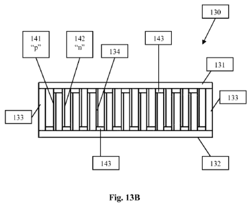
[000100] Figs. 13A-B illustrates one possible configuration of a
thermoelectric
device 130 useful for energy harvesting. Device 130, as shown, includes a top
plate 131 and a bottom plate 132, both of which may be made from, in an
embodiment, heat-conducting alumina, such as aluminum nitride. In one
embodiment, top plate 131, for instance, can act as a hot surface for
collecting
heat energy, while the bottom plate 132 can act as a cool surface for
dissipating
heat energy from the top plate 131. Thermoelectric device 130 also includes
supports 133 situated between top plate 131 and bottom plate 132. Supports
133, in one embodiment, may be made from a low-thermal-conductivity
material, such as Torlon. Device 130 further includes a core 134 situated
between supports 133 and extending from the top plate 131 to the bottom plate
132. In an embodiment, core 134 may be provided with a design such as that
illustrated in Fig. 14. Specifically, core 134 may include a nanotube sheet
having one segment doped with a p-type dopant and an adjacent segment doped
with an n-type dopant, in an alternating pattern to provide a linear array 140
of
alternating p-type elements 141 and n-type elements 142. Moreover, as
illustrated, between adjacent p-type element 141 and n-type element 142, a
conducting element 143 can be provided to join the p-type element 141 with the
n-type element 142. Furthermore, one end of linear array 140 can be designed
to act as a positive contact, while the opposite end can act as a negative
contact
(See Fig. 13A).
[000101] With particular reference now to Fig. 13B, in the embodiment shown,
the core 134 can include a series of nine alternating "n" and "p" type thermal
elements 141 and 142 made from a carbon nanotube sheet. The nanotube sheet,
in one embodiment, can be folded accordion style and placed between the
supports 133, such that every other conducting element 143 is in contact with
the hot top plate 131, while each of the remaining adjacent conducting
elements
143 is in contact with the cool bottom plate 132.
CA 02696013 2010-02-09
WO 2009/023776 PCT/US2008/073170
[000102] Although shown with nine alternating "n" and "p" type elements, it
should be appreciated that, if desired, core 134 can be made to have more than
or less than the nine alternating "n" and "p" type elements shown. Moreover,
rather than just one nanotube sheet, a plurality of nanotube sheets having
alternating "n" and "p" type elements may be used. When utilizing a plurality
of nanotube sheets, each sheet may be placed on top of one another, or each
sheet placed adjacent to and in parallel to one another, or both. Regardless
of
the arrangement of the sheets, when using a plurality of sheets, the mass of
core
134 can increase, which can result in more power output in the thermoelectric
device 130.
[000103] To provide the doped pattern in array 140, in one embodiment, the n-
type elements 142 may be doped (i.e., chemically treated) with chemicals or
chemical solutions that can act as electron donors when adsorbed onto the
surface of the nanotubes, making the resulting n-type elements 142 electron-
doped. Examples of such chemicals or chemical solutions include
polyethylenimine (PEI) and hydrazine. Other chemicals or chemical solutions
can also be used. Of course, traditional doping protocols may instead be used.
[000104] Table IV illustrates solutions used and their effect on carbon
nanotube
materials.
26
CA 02696013 2010-02-09
WO 2009/023776 PCT/US2008/073170
Table IV
Seebeck
after
Starting Ending Secondary
Seebeck Seebeck Secondary Treatment
Sample # Treatment (uV/K) (uV/K) Treatment (uV/K)
Polyethylenimine (PEI,
H(NHCHzCHz)nNHz) 20 wt% in Bake 2 hr @
1 EtOH 32 -58 250 C 75
Tri-octyl phosphene (TOP,
3a [CH3(CH2)7]3P) 20 wt% in EtOH 32 -14
Tri-octyl phosphene (TOP) 20 wt% Bake 2 hr @
3b in Hexane 32 -62 325 C 70
3c 100% TOP 32 -61
Tri-phenyl phosphine 20 wt% in
4a acetone 32 -15
Hydrazine, NH2NH2
6 Ammonia, NH3
7 Aniline, C6H5NH2
8 Sodium Azide, NaN3
9 Melamine, C3H6N6
Acetonitrile, CH3CN
11 Benzylaime, C6H5CH2NH2
Polyvinylpyrrolidone ((PVP,
12 (C6H9NO)n)
Methylpyrrolidone (NMP,
13 CsH9NO)
14 Polyaniline
Amino butyl phosphonic acid
[000105] In one embodiment, treatment of n-type elements 142 can be as
follows.
Strips of copper 143 are electroplated onto the a carbon nanotube sheet to
divide
it into distinct sections. Every other section, in an embodiment, can be doped
to
n-type 142, as shown in Fig. 14. The sections to be n-type are then treated
with
a concentrated electron-rich solution of one of the chemicals listed in Table
IV.
After the n-type sections are carefully rinsed, the strip is folded, accordion-
style
and soldered between the two alumina plates 131 and 132. The Seebeck
coefficient produced from the "n" and "p" type sections is, respectively, -60
V/ K and 70 V/ K, which gives a total of 130 V/ K per element.
[000106] This device can also be used as a Peltier device, using the flow of
electrons or holes within the thermoelectric material to pump heat from one
side
27
CA 02696013 2010-02-09
WO 2009/023776 PCT/US2008/073170
of the device to the other. The internal thermoelectric element can be
modified
slightly from the energy harvesting version to increase the efficiency. The
treatment remains the same as above with the exception that a multi-layered
piece of nanotube material may be used (thickness of about 1-2 mm) with the
nanotube materials placed on top of one another. Short, square elements can
then be cut from the treated nanotube material and soldered between the
alumina plates, thus increasing the contact area between the thermoelectric
material and the alumina.
Advantages
[000107] Advantages of the thermal and conductive elements used in
thermoelectric device of the present invention include:
[000108] = High semiconductor transition temperature of up to 600 C.
[000109] = High power output of greater than 1 W/g to 3W/g at a 400 C
difference in temperature.
[000110] = Substantially light in weight and low cost when compared with
the commercially available semiconductor material in large volumes.
[000111] = Voltages can be tailored by increasing the number of elements in
an array.
Applications
[000112] The thermoelectric device or generator of the present can be utilized
for
a number of other applications. Among these, devices can be manufactured for
applications including: (1) A solar battery charger (2) A high energy light
weight transient thermal battery replacement placed in rockets or missiles,
(3) A
low temperature energy harvester suitable for body heat battery charging or
applications used at very low temperatures, such as sub-zero (i.e., below 0
C)
or temperatures in space or in Arctic or Antarctic environments, and (4) a 1
Mega-Watt thermal generator.
[000113] Light weight thermoelectric devices can also be manufactured in
combination with solar cells to capture the waste heat radiated to space.
These
devices can be designed to operate at a temperature of about 370 K and
radiate
28
CA 02696013 2010-02-09
WO 2009/023776 PCT/US2008/073170
to about a 50 K background. This very large AT should enable the capture of
significant amounts of now wasted power and allow the solar arrays to operate
at a reduced temperature thereby improving their efficiency.
[000114] Carbon nanotube thermoelectric devices of the present invention can
further be used in conjunction with waste heat from satellites, communication
electronics, and power systems, for power harvesting and thermal management
purposes. An example may be a body heat powered device used for charging
batteries. In particular, carbon nanotube thermoelectric blanket power sources
could replace delicate, heavy, and expensive GaAs cell and coated cover glass
components in photovoltaic arrays, so as to eliminate the costly multi-step
assembly. This in turn would permit improved on-station altitude control and
reduced propellant usage for either lower launch costs or extended mission
operations. Future civil and defense spacecraft may also need more efficient,
higher power sources and improved thermal management systems in order to
meet escalating mission performance goals. As such, the thermoelectric devices
of the present invention can be used for such purposes
[000115] Another example may be to use the thermoelectric devices of the
present
invention in conjunction with various machines, electronic devices, power
systems that generate waste heat. The present invention contemplates using the
thermoelectric devices to harvest the waste heat, converting the waste heat to
power, and redirecting the power to these machines, devices or systems for
reused, so as to enhance efficiency and reduce overall power usage.
[000116] Moreover, whether used for megawatt-class space-based radar
platforms, radio isotope thermoelectric generator (RTG) powered deep space
exploration missions, or orbiting nanosat clusters, a high specific power
technology such as that offered by the thermoelectric power generators can be
a
key enabler in each mission area and can provide a strong competitive
advantage.
[000117] Ground-based devices can also be designed from the thermoelectric
element of the present invention.
29
CA 02696013 2010-02-09
WO 2009/023776 PCT/US2008/073170
[000118] While the present invention has been described with reference to
certain
embodiments thereof, it should be understood by those skilled in the art that
various changes may be made and equivalents may be substituted without
departing from the true spirit and scope of the invention. In addition, many
modifications may be made to adapt to a particular situation, indication,
material and composition of matter, process step or steps, without departing
from the spirit and scope of the present invention. All such modifications are
intended to be within the scope of the claims appended hereto.