Note: Descriptions are shown in the official language in which they were submitted.
CA 02696119 2010-02-10
Chip Module For An RFID System
The invention relates to a chip module for an RFID system, an
RFID system with the chip module and a self-adhesive RFID label,
as well as a method for producing same.
When producing RFID labels, so-called chip modules are used which
have an RFID microchip and electric connection contacts with
which they are connected to an antenna. The German Patent
Application 10 2006 052 517 describes a generic chip module in
which an RFID chip and a coupling antenna which is electrically,
in particular galvanically, connected with the RFID chip is
arranged on a web-like support material. RFID labels are
produced using the chip module, wherein a chip module arranged on
a support foil is positioned and glued onto a flat secondary
antenna such that the coupling antenna and the RFID antenna are
inductively coupled.
In the German Patent Application 10 2007 026 720, a self-adhesive
antenna for an RFID system is described which is punched out of
an aluminum foil having a thickness of 1 m - 20 m, in
particular of about 10 m, and is glued onto the front side of an
adhesive material.
The object of the invention is to create a generic chip module
which enables the production of an environmentally friendly RFID
system comprising primarily recyclable materials such as aluminum
CA 02696119 2010-02-10
2
and paper.
This object is solved with the features of claim 1.
According to claim 2, an adhesive material comprising a support
layer of paper is advantageous as the web-like or sheet-like
support material.
The coupling antenna can be cut, in particular punched, out of an
aluminum foil in a cost-effective and environmentally friendly
manner, as claimed in claim 3. Alternatively, it is also
possible to imprint the coupling antenna with an aluminum-
containing printing ink.
Claims 5 to 9 comprise preferred, there especially preferred,
embodiments of an RFID system in which the coupling antenna and a
secondary antenna of the system are inductively coupled.
Especially advantageously, the secondary antenna is also made of
recyclable aluminum and the antenna foil for the secondary
antenna is an adhesive material having a support layer also made
of recyclable paper. This also simplifies the production of the
system as the number of materials used is limited.
The self-adhesive RFID label according to claim 10 can be
advantageously made in a simplified manner since the same
material is used for the inlay material, including its adhesive
layer, as used for the cover material with the associated
adhesive layer of the label.
An RFID label according to claim 11 can be made especially
advantageously if an adhesive material with a support layer
comprised of paper is used for all support materials, whereby the
paper can be recycled in an environmentally friendly manner.
CA 02696119 2010-02-10
3
Claims 12 and 13 contain especially advantageous methods for
producing a chip module according to the invention.
The invention will be described in greater detail in the
following with reference to examples of embodiments, wherein the
same features in the various embodiments are provided with the
same reference numbers. Alternative features will be
differentiated by the additions "a" and "b".
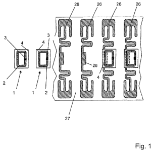
Fig. 1 shows a chip module which is fastened to a support foil
and its positioning on a secondary antenna.
Fig. 2a schematically shows a method for producing the coupling
antennas for the chip module.
Fig. 2b schematically shows an alternative method.
Fig. 3a shows, in a top view, the individual production steps
of the coupling antenna in the method according to Fig.
2a.
Fig. 3b shows the production steps in the alternative method
according to Fig. 2b.
Fig. 4 shows the structure of the aluminum/adhesive composite
material from which the coupling antennas are produced.
Fig. 5 shows the punching out of the coupling antennas.
Fig. 6 shows a section through a chip module.
Fig. 7a shows the section C-C of Fig. 6 in a first embodiment.
CA 02696119 2010-02-10
4
Fig. 7b shows the section C-C of Fig. 6 in a second embodiment.
Fig. 8 shows the strip-like arrangement of the coupling
antennas before the chip is fastened to them.
In Fig. 1, two chip modules 1 are shown which each comprise a
coupling antenna 2 and an RFID chip 3 arranged on the coupling
antenna 2. The RFID chip 3 is electrically, in particular
galvanically, connected with the coupling antenna. The coupling
antenna 2 with the RFID chip 3 is arranged on the upper side of a
web-like or sheet-like support material 4. On its lower side,
the support material 4 has an adhesive layer 10 which is covered
by a removable web-like or sheet-like separating material 6,
preferably a silicone paper.
The coupling antenna 2 consists of an aluminum layer having a
thickness of 1 m - 20 m, in particular of 3 m - 12 m. In the
embodiment, the thickness of the aluminum layer is about 10 m.
Preferably, the coupling antenna 2 is cut out of an aluminum foil
7 of corresponding thickness. This can be accomplished, as shown
in the example, by punching out or by cutting with a laser beam.
Alternatively, it is also possible to imprint the coupling
antenna 2 on the support material 4 with an aluminum-containing
ink.
The support material 4 contains a support layer which is
preferably made of paper. The support material 4 can also be
made of a plastic such as PP or PE. Preferably, a web-like or
sheet-like aluminum/adhesive composite material, whose
structure/composition is shown in Fig. 4, is used as starting
material for the production of the chip module.
An aluminum foil 7 is securely glued to the upper side of a web-
CA 02696119 2010-02-10
like or sheet-like support material 4 of paper by means of an
adhesive layer 9. A separating foil composed of silicone paper 6
is removably glued to the lower side of the paper layer 4 by
means of an adhesive layer 10. The coupling antennas 2 are first
punched out of this aluminum/adhesive composite material in the
manner described in the following.
The aluminum/adhesive composite material is comprised of an
aluminum foil 7 having a thickness of 1 m - 20 m, in particular
3 m - 12 m, in the example about 10 m, a support material of
paper having a thickness of between 50 g/m2 - 90 g/m2, in the
example 70 m, and a separating foil of silicone paper having a
thickness of 50 m - 60 m. The adhesive layer 9 under the
aluminum foil 7 has a thickness of 3 m - 7 m, in the example
about 5 m, and the adhesive layer 10 on the lower side of the
paper support foil 4 has a thickness of between 15 m and 25 m,
in the example 20 m.
As shown in Fig. 2a, the aluminum/adhesive composite material is
removed from a roll 11 by means of advancing rollers 12 and
delivered to a subsequent punching machine 13. The inner contour
14 of the coupling antenna 2 is punched out by means of the
punching machine 13 with a cut through all layers of the
aluminum/adhesive composite material. As can be seen on the left
in Fig. 3a, a hole defined by the inner contour 14 is then found
in the middle of a strip in the composite material. The cutting
waste produced during punching is removed, drawn off by suction
in the example. In a subsequent further punching device 15, the
contact point 16a for the RFID chip is then punched out. With
this punching, the cut extends at least through the aluminum foil
7 and the adhesive layer 9 found below it, whereby the support
material 4 is not completely cut through. The object of this
CA 02696119 2010-02-10
6
punching step is to cut the previously self-contained coupling
antenna 2 open by means of a separating cut, so that an
electrical short circuit does not occur. At the same time, a
non-conductive zone is cut out of the aluminum foil 7 in which
so-called supporting bumps of the chip 3 can be arranged. The
areas exposed in the aluminum foil 7 during this punching process
are shown in Fig. 7a.
Following the punching device 15, a further punching device 18a
is arranged by means of which the outer contour 19 of the
coupling antenna 2 is cut out. In this punching process, the cut
extends up to the separating foil 6. The punching processes for
the contact point and for the outer contour are shown in two
steps in Fig. 2a. However, the two punching processes can also
be carried out with a single rotating tool, as shown in Fig. 5.
The punching tool 20 comprises two punch knives 21, 22 which cut
to varying depths, wherein the punch knife 21 cuts out the
contact point 16 with a cut that extends up to the paper 4 used
as support material, and the punch knife 22 cuts out the outer
contour with a cut which extends to the separating foil 6.
After the punching in the punching device 18a, the punch grid is
removed and wound on a roll 23. The separating foil 6 with the
coupling antenna 2 found thereon is wound into a roll 24. As
shown in Fig. 8, the coupling antennas 2 are arranged at a
distance behind one another on the separating foil 6. The latter
is, in turn, made in the form of strips, so that the coupling
antennas 2 can be delivered in several tracks and behind one
another in each case to the subsequent processing. An RFID chip
3 is fastened to each coupling antenna 2 in the subsequent
processing step, as shown in Fig. 6.
An alternative method is shown in Fig. 2b in which the inner
CA 02696119 2010-02-10
7
contour 14 and the outer contour 19 of the coupling antenna 2 is
punched out in one cut which extends to the separating foil 6.
The inner contour 14 is thereby taken along by the punch cylinder
18b and drawn off by suction and can then be disposed of. The
contact point 16 for the RFID chip 3 is then punched out in the
punching device 15, which, as a straight cut 16 b, thus forms a
straight separating line according to this embodiment, as shown
in Figs. 3b and 7b.
As shown in Figs. 6 and 7a, 7b, the aluminum foil 7 represents
the conductor path of the coupling antenna 2 in the uppermost
layer. When furnished with chips 3, the chip feet, called
"bumps" 17 are pressed into the aluminum foil 7 and, optionally,
into the adhesive layer 9 below it. In this way, a certain
positive locking for the galvanic contacting of the bumps 17 is
produced. An adhesive 25, which holds the chip 3 in position, is
applied with the contact points of the coupling antenna 2 prior
to being equipped. This adhesive 25 is usually an expensive
conductive adhesive having silver particles as conductive
substance..
An embodiment is shown in Fig. 7a in which the contact point 16a
comprises a perhaps semicircular recess which is punched out of
the aluminum foil 7. The contact of the aluminum foil 7 with the
RFID chip takes place via the lower bumps 17a which are
electrically separated from one another by a further separating
cut 16a in the aluminum foil 7 to prevent an electrical short
circuit.
An advantageous alternative possibility is shown in Fig. 7b, as
to how to form the contact point 16 between the coupling antenna
2 punched out of the aluminum foil 7 and the RFID chip 3. In
this embodiment, the two upper bumps 17 only have a function of
CA 02696119 2010-02-10
8
supporting the chip 3, they are not connected with the chip so as
to be electrically conductive. The electrical contact is made
via the two lower bumps 17a. The two contact bumps 17a are
electrically separated from one another by a straight cut 16b.
When punching out the straight cut 16b, the two edges of the foil
7 are flanged apart, so that a separating line forms which safely
prevents a contact. In the event that it is required for the
insulation effect, an insulating adhesive can, in addition, be
pressed into the separating line 16b which securely keeps the two
edges of the foil 7 apart after hardening. Advantageously, this
plastic can be simultaneously used to securely fasten the bumps
17 and thus the RFID chip 3 to the foil 7.
The invention makes it possible to replace the adhesive 25 by a
non-conductive, cost-effective adhesive. Attention must be paid
to the fact that a possibly appearing oxide layer of the aluminum
at the contact points of the coupling antenna 2 does not impede
the electric contact in a troublesome manner. To prevent the
appearance of a troublesome oxide layer from the start, a very
thin layer of protective lacquer can be applied over the aluminum
foil 7 as oxidation protection. With respect to its consistency
and its adhesion to the aluminum, the protective lacquer is
selected such that it breaks open when contacting, i.e. when the
chip 3 is placed on the contact points of the coupling antenna 2
and releases a non-oxidized contact surface for a galvanic
connection.
The chip module 1 with the chip 3 can already be used as an RFID
system in a very narrow short-range area, since the coupling
antenna 2 acts as UHF antenna. For greater ranges, the chip
module 1 is positioned and glued with its support material 4 to a
flat secondary antenna 26 in such a manner that the coupling
antenna 2 and the secondary antenna 26 are inductively coupled.
CA 02696119 2010-02-10
9
The secondary antennas 26 are thereby arranged on the upper side
of a support material, whereby an adhesive material with a paper
support layer is thereby preferably used as support material.
Alternatively, a plastic such as PE or PP can also be used for
the support layer. Preferably, as shown in Fig. 1, the adhesive
layer of the support material is covered by a web-like or sheet-
like separating material 27. The secondary antennas 26 are thus
arranged on the upper side of the separating material 27.
Preferably, the secondary antenna 26 is also made from an
aluminum layer having a thickness of 1 m - 20 m, in particular
of 3 m - 12 m, in the example about 10 m. Similar to the
coupling antenna 2, the secondary antenna 26 is thereby
preferably cut out, in particular punched out, of an aluminum
foil of corresponding thickness. Preferably, an adhesive with a
paper support layer is used as support material for the secondary
antenna 26 in the same way as for the coupling antenna 2, to keep
the number of materials used low and to use, if necessayr, the
same materials.
The RFID systems consisting of the chip module and secondary
antenna are preferably used to produce self-adhesive RFID labels.
An RFID system is thereby used as an RFID inlay between a web-
like or sheet-like cover material which is provided with an
adhesive layer on the lower side and a web-like or sheet-like
support material which can be removed from the adhesive layer.
Preferably, the same material is thereby used as support material
for the RFID inlay, including its adhesive layer, as for the
cover material with the adhesive layer of the label. It is
especially preferred to use an adhesive material with a paper
support layer for all support materials. In this way, only paper
and aluminum are used for the production of the RFID label,
aluminum being for the antennas.