Note: Descriptions are shown in the official language in which they were submitted.
CA 02696704 2010-02-17
WO 2009/025700 PCT/US2008/008089
RFID ANTENNA FOR USE ADJACENT TO CONDUCTIVE ELEMENTS
FIELD OF THE INVENTION
The present invention relates to radio frequency identification (RFID) tag
antennas,
and more particularly to RFID tag antennas which are operable when adjacent to
metal
and other conductive elements.
BACKGROUND OF THE INVENTION
Accurately monitoring of the location and flow of the objects associated with
inventory, product manufacturing, merchandising, and related operations is
challenging.
There is a continuing need to determine the location of these objects and to
track relevant
information about the objects. A tag, marker or label device suitably
configured to be
associated with any of a variety of objects, including goods, items, persons,
or animals, or
substantially any moving or stationary and animate or inanimate object, which
facilitates
location and data tracking, can be used. One such tag tracking system is an
electronic
identification system, such as RFID. RFID tags are affixed to, connected to,
or in some
way associated with an object for the purpose of tracking the object, and
storing and
retrieving information about the object.
The RFID tag stores data associated with the object. A RFID reader may scan
for
RFID tags by transmitting an interrogation signal at a known frequency. The
RFID tags
may respond to the interrogation signal with a response containing, for
example, data
associated with the object or a RFID tag ID. The RFID reader detects the
response signal
and decodes the data or the RFID tag ID. The RFID reader may be a handheld
reader, or a
fixed reader by which items carrying a RFID tag pass. A fixed reader may be
configured
as an antenna located in a pedestal similar to those used in an electronic
article
surveillance ("EAS") system.
1
CA 02696704 2010-02-17
WO 2009/025700 PCT/US2008/008089
Antennas collect and emit energy in the form of electromagnetic waves. The
units
for this transfer take the form of power-per-unit area. Many tags for use in
such tag
detection systems have a single favored orientation with respect to the
stimulating field
where they exhibit a maximum response, i.e., they are directional. Most tags
are
somewhat rectangular in shape and are variations of a dipole antenna, with a
high length-
to-width ratio. These tags give a maximum response when oriented within an
incident
field orthogonal to the long axis of the tag. This property is commonly
referred to as "read
orientation sensitivity".
For example, FIG. 1 illustrates an example of a RFID tag 100 with an antenna
102
disposed upon substrate 104. Substrate 104 is substantially rectangular in
shape. The
antenna 102 comprises multiple antenna portions, i.e., antenna 102 has a first
antenna
portion 106 and a second antenna portion 108. The first antenna portion 106 is
connected
to a first side 112A of lead frame 112. Second antenna portion 108 may be
connected to a
second side 112B of lead frame 112. RFID chip 110 may be connected to lead
frame 112
by ultrasonically bonding lead frame 112 to the conductive pads on RFID chip
110. RFID
chip 110 and lead frame 112 are placed directly in the geometric center of the
dielectric
substrate material of substrate 104. The ends of lead frame 112 can be
physically and
electrically bonded to the foil antenna pattern of antenna 102. The RFID chip
also can be
bonded directly to antenna 102 at the conductive pads by use of conductive
adhesive to
eliminate the need for lead frame 112.
The first antenna portion 106 has a first antenna end 106A and a second
antenna
end 106B. Similarly, second antenna portion 108 has a first antenna end 108A
and a
second antenna end 108B. The first antenna end 106A of first antenna portion
106 is
connected to lead frame 112A. First antenna portion 106 is disposed on
substrate 104 and
forms an inwardly spiral pattern from RFID chip 110 in a first direction, with
second
2
CA 02696704 2010-02-17
WO 2009/025700
PCT/US2008/008089
antenna end 106B to terminate on the inner loop of the inwardly spiral pattern
on one half
of the substrate 104. Similarly, first antenna end 108A of second antenna
portion 108 is
connected to lead frame 112B. Second antenna portion 108 is disposed on
substrate 104
to form an inwardly spiral pattern from RFID chip 110 in a second direction,
with second
antenna end 108B to terminate on the inner loop of the inwardly spiral pattern
on the other
half of the substrate 104. As illustrated in FIG. 1, the two clockwise spiral
sections 106,
108 of antenna 102 basically are rotationally symmetrical with respect to each
other. The
RFID tag 100 generates a radiation pattern 200 (FIG.2) similar to the
radiation pattern of a
conventional dipole antenna.
The RFID tag 100 receives and emits best when perpendicular (e.g., along the z-
axis) to its y-axis and not at all along that y-axis (also referred to as the
"dipole axis"), as
illustrated by the radiation pattern 200 graph of FIG. 2. The dead area in the
radiation
pattern 200 of the antenna 102 is referred to as a null 202. Antenna
directivity is
important for RFID tags because if the tag 100 is oriented where its null 202
is pointed at
the tag reader, the tag 100 receives no power for excitation and therefore is
not read. In
general, the radiation pattern describes the sensitivity of the receiving
antenna to the
direction of travel or the propagation of an electromagnetic (EM) wave. Since
the EM
wave is a transverse wave, the E-field component of the EM wave is
perpendicular to the
direction of the wave propagation.
Another situation that causes additional null regions in the radiation pattern
200 of
the tag antenna 102 is when the RFID tag 100 is applied to a conductive
surface, e.g., a
metal surface. In order to couple energy into a "dipole-like" antenna, an
excitation field
("E-field") parallel to the length of the dipole-like antenna that has the
proper frequency is
required. The conductive nature of the metal dictates that the tangential e-
field, which is
aligned with length of the dipole, will be zero on the metal surface. This
effect prevents
3
CA 02696704 2010-02-17
WO 2009/025700
PCT/US2008/008089
coupling of energy into the RFID tag 100, which causes a full or partial
degradation of the
detection performance of the RFID tag 100.
Once removed from the surface of the metal, the electric field can be non-
zero.
Therefore, a dielectric spacer, which provides separation between the dipole
antenna and
the metal surface, enables some degree of an excitation field reaching the
RFID tag 100.
However, a large spacer, e.g., larger than ten millimeters, is required even
for ultra-high
frequency (UHF) RFID tags to regain comparable exposure to the excitation
field, and
thus making the packaging and application impractical. In addition, the
typical dielectric
spacer is relatively expensive.
In view of the above, it is desirable to provide a RFID device having a
radiation
pattern that is minimally affected by a conductive surface, such as a metal
surface, EAS
tag, etc.
SUMMARY OF THE INVENTION
The present invention advantageously provides a radio frequency identification
(RFID) system and RFID tag for operation with conductive elements.
In accordance with one aspect, the present invention provides a RFID tag for
use
with conductive elements that includes a substrate body having a surface and
defining a
plane of the tag. A RFID integrated circuit is disposed on the surface of the
substrate
body. An antenna that has an antenna pattern is disposed on the substrate body
and is in
electrical communication with the RFID integrated circuit. The antenna
generates a
radiation pattern with maximum gain along an axis that is substantially
coplanar with the
tag. The antenna can include a first antenna portion and a second antenna
portion. The
first antenna portion has a first antenna end and a second antenna end. The
first antenna
end of the first portion is in electrical communication with the RFID
integrated circuit.
4
CA 02696704 2010-02-17
WO 2009/025700 PCT/US2008/008089
The first antenna portion forms an antenna pattern in a counterclockwise
direction. The
second antenna portion has a first antenna end and a second antenna end. The
first
antenna end of the second antenna portion is in electrical communication with
the RFID
integrated circuit. The second antenna portion forms an antenna pattern in a
clockwise
direction. The second antenna portion has a first antenna end and a second
antenna end,
the first antenna end of the second antenna portion is in electrical
communication with the
RFID integrated circuit. The second antenna portion forms an antenna pattern
in a
clockwise direction.
In accordance with another aspect, the present invention provides a RFID
system
for use with conductive elements that includes a RFID reader that generates
interrogation
signals, and a security tag to receive the interrogation signal and transmit a
response
signal. The security tag includes a substrate body having a surface and
defining a plane of
the tag. A RFID integrated circuit is disposed on the surface of the substrate
body. An
antenna that has an antenna pattern is disposed on the substrate body and is
in electrical
communication with the RFID integrated circuit. The antenna arranged to
generate a
radiation pattern with maximum gain along an axis that is substantially
coplanar with the
tag.
In accordance with another aspect, the present invention provides a RFID tag
for
use with conductive elements that includes a substrate body having a surface
and defining
a plane of the tag, a RFID integrated circuit disposed on the surface of the
substrate body,
a conductive element, the conductive element proximate the substrate body, and
an
antenna that has an antenna pattern. The antenna is disposed on the substrate
body and in
electrical communication with the RFID integrated circuit, the antenna
arranged to
generate a radiation pattern with maximum gain along an axis that is
substantially coplanar
with the tag.
5
CA 02696704 2015-04-28
77496-331
According to another aspect of the present invention, there is provided a
radio
frequency identification (RFID) tag, the tag comprising: a substrate having a
surface, the
substrate defining a plane of the tag; a RFID integrated circuit disposed on
the surface of the
substrate; and an antenna having an antenna pattern, the antenna disposed on
the substrate and
in electrical communication with the RFID integrated circuit, the antenna
arranged to generate
a radiation pattern with maximum gain along an axis that is substantially
coplanar with the
tag, wherein the antenna includes a first antenna portion and a second antenna
portion, the
first antenna portion having a first antenna end and a second antenna end, the
first antenna end
of the first antenna portion in electrical communication with the RFID
integrated circuit and
the first antenna portion forming an antenna pattern in a counterclockwise
direction, and the
second antenna potion having a first antenna end and a second antenna end, the
first antenna
end of the second antenna portion in electrical communication with the RFID
integrated
circuit and the second antenna portion forming an antenna pattern in a
clockwise direction,
wherein the substrate has a first edge, a second edge opposite the first edge,
a third edge, and a
fourth edge opposite the third edge, the third and fourth edges are longer
than the first and
second edges; wherein the RFID integrated circuit is positioned at a midpoint
of the fourth
edge of the substrate.
According to another aspect of the present invention, there is provided a RFID
system, the system comprising: a radio frequency identification reader
generating
interrogation signals; and a security tag to receive the interrogation signal
and transmit a
response signal, the security tag comprising the features as described herein.
According to another aspect of the present invention, there is provided an
radio
frequency identification (RFID) tag, the tag comprising: a substrate having a
first surface and
a second surface opposite to the first surface, the substrate defining a plane
of the tag; a
conductive element disposed on the first surface of the substrate; an RFID
integrated circuit
disposed on the second surface of the substrate; and an antenna having an
antenna pattern, the
antenna disposed on the second surface of the substrate and in electrical
communication with
the RFID integrated circuit, the antenna having a first clockwise dipole
element forming a first
spiral and a second counterclockwise dipole element forming a second spiral,
the antenna and
the conductive element arranged to generate a radiation pattern having a
maximum gain along
6
CA 02696704 2015-04-28
77496-331
an axis that is substantially coplanar with the plane of the tag that is
greater than a maximum
gain along an axis that is substantially orthogonal to the plane of the tag,
the radiation pattern
exhibiting a null substantially orthogonal to the plane of the tag.
According to another aspect of the present invention, there is provided a RFID
system, the system comprising: a radio frequency identification reader
generating
interrogation signals; and a security tag to receive the interrogation signal
and transmit a
response signal, the security tag comprising: a substrate having a first
surface and a second
surface opposite to the first surface, the substrate defining a plane of the
tag; a conductive
element disposed on the first surface of the substrate; an RFID integrated
circuit disposed on
the second surface of the substrate; and an antenna having an antenna pattern,
the antenna
disposed on the second surface of the substrate and in electrical
communication with the
RFID integrated circuit, the antenna having a first clockwise dipole element
forming a first
spiral and a second counterclockwise dipole element forming a second spiral,
the antenna and
the conductive element arranged to generate a radiation pattern having a
maximum gain along
an axis that is substantially coplanar with the plane of the tag that is
greater than a maximum
gain along an axis that is substantially orthogonal to the plane of the tag,
the radiation pattern
exhibiting a null substantially orthogonal to the plane of the tag.
According to another aspect of the present invention, there is provided an
radio
frequency identification (RFID) tag, the tag comprising: a substrate having a
first surface and
a second surface opposite to the first surface, the substrate defining a plane
of the tag; a
conductive element disposed on the first surface of the substrate; an RFID
integrated circuit
disposed on the second surface of the substrate; and an antenna having an
antenna pattern, the
antenna disposed on the second surface of the substrate and in electrical
communication with
the RFID integrated circuit, the antenna having a first clockwise dipole
element forming a first
spiral and a second counterclockwise dipole element forming a second spiral,
the combined
antenna and conductive element generating a radiation pattern having a maximum
gain along
an axis that is substantially coplanar with the plane of the tag that is
greater than a maximum
gain along an axis that is substantially orthogonal to the plane of the tag,
the radiation pattern
exhibiting a null substantially orthogonal to the plane of the tag.
6a
CA 02696704 2015-04-28
77469-331
Additional aspects of the invention will be set forth in part in the
description which
follows, and in part will be obvious from the description, or may be learned
by practice of
the invention. The aspects of the invention will be realized and attained by
means of the
elements and combinations particularly pointed out in the appended claims. It
is to be
understood that both the foregoing general description and the following
detailed
description are exemplary and explanatory only and are not restrictive of the
invention, as
claimed.
6b
CA 02696704 2010-02-17
WO 2009/025700 PCT/US2008/008089
BRIEF DESCRIPTION OF THE DRAWINGS
A more complete understanding of the present invention, and the attendant
advantages and features thereof, will be more readily understood by reference
to the
following detailed description when considered in conjunction with the
accompanying
drawings wherein:
FIG. 1 is a diagram of a conventional RFID tag;
FIG. 2 is a diagram illustrating an example of a three-dimensional radiation
pattern
of the conventional tag antenna of FIG. 1;
FIG. 3 is a diagram of a RFID system constructed in accordance with the
principles
of the present invention;
FIG. 4 is a diagram of another embodiment of a RFID system constructed in
accordance with the principles of the present invention;
FIG. 5 is a diagram of an exemplary tag having an antenna constructed in
accordance with the principles of the present invention;
FIG. 6 is a diagram illustrating an example of a three-dimensional radiation
pattern
of the antenna of the tag of FIG. 5 constructed in accordance with the
principles of the
present invention;
FIG. 7 is a diagram of another exemplary tag having an antenna constructed in
accordance with the principles of the present invention; and
FIG. 8 is a diagram illustrating an example of a three-dimensional power gain
radiation pattern of the antenna of the tag of FIG. 7 constructed in
accordance with the
principles of the present invention.
7
CA 02696704 2010-02-17
WO 2009/025700 PCT/US2008/008089
DETAILED DESCRIPTION OF THE INVENTION
Referring now to the drawing figures in which like reference designators refer
to
like elements, there is shown in FIG. 3 a diagram of an exemplary system
constructed in
accordance with the principles of the present invention and designated
generally as "300".
Communication system 300 provides an electronic identification system in the
embodiment described herein. Further, the described communication system 300
is
configured for backscatter communications as described in detail below. It is
contemplated that other communication protocols can be utilized in other
embodiments.
The depicted communication system 300 includes at least one reader 302 having
at
least one electronic wireless remote communication device 306. Radio frequency
(RF)
communications can occur between a reader 302 and remote communication devices
306
for use in identification systems and product monitoring systems as exemplary
applications.
Remote communication devices 306 include radio frequency identification (RFID)
devices in the embodiments described herein. Multiple wireless remote
communication
devices 306 typically communicate with reader 302 although only one such
device 306 is
illustrated in FIG. 3.
Although multiple communication devices 306 can be employed in communication
system 300, there is typically no communication between the multiple
communication
devices 306 themselves. Instead, the multiple communication devices 306
communicate
with reader 302. Multiple communication devices 306 can be used in the same
field of
reader 302, i.e., within the communication range of reader 302. Similarly,
multiple
readers 302 can be in proximity to one or more of devices 306.
Remote communication device 306 is configured to interface with reader 302
using
a wireless medium in one embodiment. More specifically, communication between
8
CA 02696704 2010-02-17
WO 2009/025700 PCT/US2008/008089
communication device 306 and reader 302 occur via an electromagnetic link,
such as an
RF link, e.g., at microwave frequencies in the described embodiment. Reader
302 is
configured to output forward link wireless communication signals 308. Further,
reader
302 is operable to receive return link wireless communication signals 310,
e.g., a reply
signal, from devices 306 responsive to the forward link communication signals
308. In
accordance with the above, forward link communication signals and return link
communication signals are wireless signals, such as radio frequency signals.
Other forms
of communication signals, such as infrared, acoustic, and the like are
contemplated.
Reader unit 302 includes at least one antenna 312 as well as transmitting and
receiving circuitry, similar to that implemented in devices 306. Antenna 312
comprises a
transmit/receive antenna connected to reader 302. In an alternative
embodiment, reader
302 can have separate transmit and receive antennas.
In operation, reader 302 transmits a forward link communication signal 308,
e.g.,
an interrogation command signal, via antenna 312. Communication device 306 is
operable to receive the incoming forward link signal 308. Upon receiving
signal 308,
communication device 306 responds by communicating the responsive return link
communication signal 310, e.g., a responsive reply signal. Communications
within system
300 are described in greater detail below.
In one embodiment, responsive return link communication signal 310, e.g., a
responsive reply signal is encoded with information that uniquely identifies
or labels the
particular device 306 that is transmitting so as to identify any object,
animal, or person
with which communication device 306 is associated. Communication devices 306
can be
RFID tags that are attached to objects or people where each tag is programmed
with
information relating to the object or person to which it is attached. The
information can
take a wide variety of forms and can be more or less detailed depending on the
needs to be
9
CA 02696704 2010-02-17
WO 2009/025700 PCT/US2008/008089
served by the information. For example, the information may include
merchandise
identification information, such as a universal product code. A tag may
include
identifying information and security clearance information for an authorized
person to
whom the tag has been issued. A tag may also have a unique serial number, in
order to
uniquely identify an associated object or person. Alternatively, a tag may
include more
detailed information relating to an object or person, such as a complete
description of the
object or person. As a further exemplary alternative, a tag may store a single
bit, in order
to provide for theft control or simple tracking of entry and departure through
the detection
of an object or person at a particular reader, without necessarily
specifically identifying
the object or person.
Remote device 306 is configured to output a reply signal within reply link
communication 310 responsive to receiving forward link wireless communication
308.
Reader 302 is configured to receive and recognize the reply signal within the
reply link
communication signal 310, e.g., return signal. The reply signal can be
utilized to identify
the particular transmitting communication device 306 and may include various
types of
information corresponding to the communication device 306 including but not
limited to
stored data, configuration data or other command information.
An exemplary embodiment of a reader 302 is explained with reference to FIG. 4.
In this embodiment, the reader 302 has a RF module or unit 400 and a
controller module
or unit 402. The RF module 400 includes a radio signal source 404 for
synthesizing radio
frequency signals, e.g., an interrogating RF signal, that outputs a RF signal
to transceiver
406 of the reader 302. The interrogating RF signal from the source 404 uses a
suitable
frequency such as 915 MHz. When the radio signal source 404 is energized,
transceiver
406 transmits the interrogating RF signal (typically after the RF signal has
been modulated
CA 02696704 2010-02-17
WO 2009/025700
PCT/US2008/008089
with an information signal) through antenna 312 to a suitable antenna 314 such
as a dipole
antenna at the wireless communication device 306.
Modulated signals are received from communication device 306 via antenna 312
and passed to transceiver 406. Controller module 402 of reader 302 receives
the digital
equivalent of the modulated signal. In one embodiment, controller module 402
produces
signals in a sequence having a pattern identifying the pattern of the l's and
O's in read
only memory ("ROM") 408 of communication device 306. For example, the received
and
processed sequence may be compared in reader 302 with a desired sequence to
determine
whether the object being identified is being sought by reader 302 or not.
Continuing to refer to FIG. 4, one embodiment of remote communication device
306 is explained. The depicted communication device 306 includes a modulator
410
having a receiver/transmitter as described below and a data source such as ROM
408,
which provides a sequence of binary l's and binary O's in an individual
pattern to identify
the object. In this embodiment, a binary "1" in ROM 408 causes a modulator 410
to
produce a first plurality of signal cycles and a binary "0" in ROM 408 causes
the
modulator 410 to produce a second plurality of signal cycles different from
the first
plurality of signals. The pluralities of signals cycles are sequentially
produced by the
modulator 410 to represent the pattern of binary l's and binary O's which
identify the
object are introduced to the dipole antenna 314 for transmission to antenna
312 at reader
302. In another embodiment, the communication device 306 can have separate
receive
and transmit antennas. Communication device 306 may further include an
optional power
source (not shown) connected to modulator 410 to supply operational power to
modulator
410.
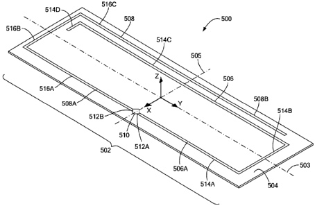
FIG. 5 illustrates a RFID tag 500 constructed in accordance with the
principles of
the present invention. In this embodiment, an antenna 502 can be disposed upon
substrate
11
CA 02696704 2010-02-17
WO 2009/025700 PCT/US2008/008089
504. Substrate 504 can be substantially rectangular in shape but also may have
various
other geometrical shapes to meet packaging and performance parameters.
Substrate 504
can define a latitudinal axis 503 that is parallel to the proximal and distal
longer edges of
substrate 504 and intersects the center point of substrate 504. Thus
latitudinal axis 503
lies along the y-axis and divides the substrate 504 into a distal half and a
proximal half.
Substrate 504 also can define a longitudinal axis 505 that is parallel to the
left and right
short edges of substrate 504 and intersects the center point of substrate 504.
Thus
longitudinal axis 505 lies along the x-axis and divides the substrate 504 into
a left half and
a right half Substrate 504 can comprise any type of material suitable for
mounting
antenna 502, optional lead frame 512, and RFID chip 510. For example, material
for
substrate 504 may include base paper, polyethylene, polyester, and so forth.
The
particular material implemented for substrate 504 may impact the RF
performance of
RFID tag 500. More particularly, the dielectric constant and the loss tangent
may
characterize the dielectric properties of an appropriate substrate material
for use as
substrate 504.
The antenna 502 can have multiple antenna portions, such as a first antenna
portion
506 and a second antenna portion 508. The first antenna portion 506 can be
connected to
a first side 512A of lead frame 512. Second antenna portion 508 can be
connected to a
second side 512B of lead frame 512. RFID chip 510 may be connected to lead
frame 512
by ultrasonically bonding lead frame 512 to the conductive pads on RFID chip
510. As
illustrated in FIG. 5, RFID chip 510 and lead frame 512 can be placed near the
proximal
longer edge of the dielectric substrate material of substrate 504. In this
embodiment,
RFID chip 510 and lead frame 512 can be placed 1 to 5 mm from the proximal
longer
edge of the substrate 504. The ends of lead frame 512 may be physically and
electrically
bonded to the antenna pattern of antenna 502.
12
CA 02696704 2010-02-17
WO 2009/025700 PCT/US2008/008089
The first antenna portion 506 can have a first antenna end 506A and a second
antenna end 506B. Similarly, second antenna portion 508 can have a first
antenna end
508A and a second antenna end 508B. The first antenna end 506A of first
antenna portion
506 is connected to lead frame 512A. The first antenna portion 506 can include
several
segments 514A, 514B, 514C and 514D to define a section of the antenna pattern
of
antenna 502. The second antenna portion 508 can include several segments 516A,
516B
and 516C to define a second section of the antenna pattern of antenna 502. In
this
embodiment, segment 514A is disposed on substrate 504 and extends outward from
RFID
chip 510 toward the right short edge of substrate 504 in a substantially
parallel direction to
the proximal longer edge of substrate 504. Segment 514B is disposed on
substrate 504
and extends outward from the end of segment 514A toward the distal longer edge
of
substrate 504 in a substantially parallel direction to the right edge of
substrate 504.
Segment 514C is disposed on substrate 504 and extends inward from the end of
segment
514B toward the left short edge of substrate 504 in a substantially parallel
direction to the
distal longer edge of substrate 504. Segment 514D is disposed on substrate 504
and
extends inward from the end of segment 514C toward the proximal longer edge of
substrate 504 in a substantially parallel direction to the left short edge of
substrate 504.
Continuing to refer to FIG. 5, segment 516A is disposed on substrate 504 and
extends outward from RFID chip 510 toward the left short edge of substrate 504
in a
substantially parallel direction to the proximal longer edge of substrate 504.
Segment
516B is disposed on substrate 504 and extends outward from the end of segment
516A
toward the distal longer edge of substrate 504 in a substantially parallel
direction to the left
short edge of substrate 504. Segment 516C is disposed on substrate 504 and
extends
inward from the end of segment 516B toward the right edge of substrate 504 in
a
substantially parallel direction to the distal longer edge of substrate 504.
In this
13
CA 02696704 2010-02-17
WO 2009/025700 PCT/US2008/008089
embodiment, segment 516C can extent substantially the full length of the
substrate 504
from the left short edge of substrate 504 to the right edge of substrate 504.
In this
embodiment, the segment 516C of second antenna portion 508 can be positioned
closer to
the distal longer edge of substrate 504 than the segment 514C of the first
antenna portion
506 and at least partially enclose the second end 506B of the first antenna
portion 506.
The segment 516C can be modified by further extension and wrapping or by
further
reduction to achieve the appropriate resonance frequency for wireless
communication.
The antenna pattern of FIG. 5 advantageously generates the antenna radiation
pattern 600 as illustrated in FIG. 6. The antenna radiation pattern 600 of tag
500 has a
direction of sensitivity in an orthogonal direction, e.g., the z-axis, to the
substrate 504
plane, e.g., the y-axis. A comparison of the graph of FIG. 6 and the graph of
FIG. 2,
illustrates that the radiation pattern 600 of tag 500 is rotated approximately
90 degrees to
the left about the x-axis as opposed to the radiation pattern 200 of tag 100.
In other words,
the null of the radiation pattern 600 is orthogonal to the plane defined by
the substrate 504.
Thus, unlike the radiation pattern 200 of conventional tag 100, the direction
of sensitivity
of tag 500, as evidenced by the null 602, is orthogonal or normal to the tag
plane.
Therefore, the effects of a conductive element or surface, e.g., a metal
surface or EAS tag
(not shown), to which the tag 500 can be attached is minimized, since the
external
excitation field couples into tag 500 along the orthogonal axis normal to the
plane defined
by the conductive element or surface.
FIG. 7 illustrates an embodiment of a RFID tag 700 constructed in accordance
with
the principles of the present invention. In this embodiment, an antenna 702
can be
disposed upon substrate 704. Substrate 704 can be similar to substrate 504 in
material and
geometric shape as described above with respect to substrate 504. Substrate
704 can
define a latitudinal axis 703 that is parallel to the proximal and distal
longer edges of
14
CA 02696704 2010-02-17
WO 2009/025700 PCT/US2008/008089
substrate 704 and intersects the center point of substrate 704. Thus
latitudinal axis 703
lies along the y-axis and divides the substrate 504 into a distal half and a
proximal half.
Substrate 704 also can define a longitudinal axis 705 that is parallel to the
left and right
short edges of substrate 704 and intersects the center point of substrate 704.
Thus
longitudinal axis 703 lies along the x-axis and divides the substrate 704 into
a left half and
a right half.
The antenna 702 can have multiple antenna portions, such as a first antenna
portion
706 and a second antenna portion 708. The first antenna portion 706 can be
connected to
a first side 712A of lead frame 712. Second antenna portion 708 can be
connected to a
second side 712B of lead frame 712. RFID chip 710 may be connected to lead
frame 712
by ultrasonically bonding lead frame 712 to the conductive pads on RFID chip
710. As
illustrated in FIG. 7, RFID chip 710 and lead frame 712 can be placed near the
proximal
longer edge of the dielectric substrate material of substrate 704. In this
embodiment,
RFID chip 710 and lead frame 712 can be placed 1 to 5 mm from the proximal
longer
edge of the substrate 704. The ends of lead frame 712 may be physically and
electrically
bonded to the antenna pattern of antenna 702.
The first antenna portion 706 can have a first antenna end 706A and a second
antenna end 706B. Similarly, second antenna portion 708 has a first antenna
end 708A
and a second antenna end 708B. The first antenna end 706A of first antenna
portion 706
is connected to lead frame 712A. The first antenna portion 706 can include
several
segments 714A, 714B, 714C, 714D and 714E to define a section of the antenna
pattern of
antenna 702. The second antenna portion 708 can include several segments 716A,
716B,
716C, 716D and 716E to define a second section of the antenna pattern of
antenna 702. In
this embodiment, segment 714A is disposed on substrate 704 and extends outward
from
RFID chip 710 toward the right edge of substrate 704 in a substantially
parallel direction
CA 02696704 2010-02-17
WO 2009/025700 PCT/US2008/008089
to the proximal longer edge of substrate 704. Segment 714B is disposed on
substrate 704
and extends outward from the end of segment 714A toward the distal longer edge
of
substrate 704 in a substantially parallel direction to the right edge of
substrate 704.
Segment 714C is disposed on substrate 704 and extends inward from the end of
segment
714B toward the center portion of substrate 704 in a substantially parallel
direction to the
distal longer edge of substrate 704. Segment 714D is disposed on substrate 704
and
extends inward from the end of segment 714C toward the proximal longer edge of
substrate 704 and segment 714A in a substantially parallel direction to the
left short edge
of substrate 704. Segment 714E is disposed on substrate 704 and extends
outward from
the end of segment 714D toward the right edge of substrate 704.
Continuing to refer to FIG. 7, segment 716A is disposed on substrate 704 and
extends outward from RFID chip 710 toward the left short edge of substrate 704
in a
substantially parallel direction to the proximal longer edge of substrate 704.
Segment
716B is disposed on substrate 704 and extends outward from the end of segment
716A
toward the distal longer edge of substrate 704 in a substantially parallel
direction to the left
short edge of substrate 704. Segment 716C is disposed on substrate 704 and
extends
inward from the end of segment 716B toward the center portion of substrate 704
in a
substantially parallel direction to the distal longer edge of substrate 704.
Segment 716D is
disposed on substrate 704 and extends inward from the end of segment 716C
toward the
proximal longer edge of substrate 704 and segment 716A in a substantially
parallel
direction to the left short edge of substrate 704. Segment 716E is disposed on
substrate
704 and extends outward from the end of segment 716D toward the left short
edge of
substrate 704. In this embodiment, the first antenna portion 706 and the
second antenna
portion 708 are substantially symmetrical.
16
CA 02696704 2010-02-17
WO 2009/025700
PCT/US2008/008089
The antenna pattern 702 illustrated in FIG. 7 can be overlaid on or
incorporated
with a conductive element or surface 718, e.g., an electronic article
surveillance ("EAS")
tag such as the UltraMax manufactured by Sensormatic Electronics Corporation,
to form
RFID tag 700, which advantageously generates the antenna radiation pattern 800
as
illustrated in FIG. 8. In this embodiment, the electronic article surveillance
device can be,
for example, a magneto-acoustic device. The antenna radiation pattern 800 of
antenna
pattern 702 overlaid on the conductive element or surface 718 has a direction
of sensitivity
in an orthogonal direction, e.g., the z-axis, to the substrate 704 plane,
e.g., the y-axis. The
field effects of the symmetrical geometry of the first antenna portion 706 and
the second
antenna portion 708 blended with the RFID chip 710 and optional lead frame 712
positioned near the proximal longer edge of substrate 704 generate a radiation
pattern with
a maximum gain that is coplanar with the tag. A comparison of the graph of
FIG. 8 and
the graph of FIG. 6, illustrates similar rotational orientation and field
strength for the
radiation patterns of tag 800 and tag 600.
A comparison of the graph of FIG. 8 and the graph of FIG. 2, illustrates that
the
radiation pattern 800 of tag 700 is rotated approximately 90 degrees to the
left about the x-
axis as opposed to the radiation pattern 200 of tag 100. In other words, the
null of the
radiation pattern 800 is orthogonal to the plane defined by the substrate 704.
Thus, unlike
the radiation pattern 200 of conventional tag 100, the direction of
sensitivity of tag 700, as
evidenced by the null 802, is orthogonal or normal to the tag plane and the
plane of the
conductive element or surface 718. Therefore, the effects of a conductive
element or
surface, e.g., a metal surface or EAS tag, to which the tag antenna 702 can be
combined,
are used to generate the desired radiation pattern 800 with a maximum gain
that is
coplanar with the tag.
17
CA 02696704 2015-04-28
77469-331
It will be appreciated by persons skilled in the art that the present
invention is not
limited to what has been particularly shown and described herein above. In
addition,
unless mention was made above to the contrary, it should be noted that all of
the
accompanying drawings are not to scale. A variety of modifications and
variations are
possible in light of the above teachings without departing from the scope of
the
invention, which is limited only by the following claims.
18