Note: Descriptions are shown in the official language in which they were submitted.
CA 02699277 2010-03-10
1
D E S C R I P T I 0 N
OPTICAL DEVICE, LAMINATE AND LABELED ARTICLE
Technical Field
The present invention relates to an optical
technique.
Background Art
An optical device including a hologram or
diffraction grating is utilized in various
applications. For example, Jpn. Pat. Appln. KOKAI
Publication No. 2005-091786 describes that an optical
device including a hologram is used for the purpose of
forgery prevention.
Disclosure of Invention
An object of the present invention is to achieve a
special visual effect.
According to a first aspect of the present
invention, there is provided an optical device
comprising a light-reflecting interface provided with a
first relief structure including first recesses or
protrusions arranged two-dimensionally, the first
relief structure emitting a first diffracted light when
illuminated with a light, and a light-transmitting
interface disposed in front of the light-reflecting
interface and having a reflectance smaller than that of
the first interface, the light-transmitting interface
CA 02699277 2010-03-10
2
being provided with a second relief structure including
second recesses or protrusions arranged two-
dimensionally, and the second relief structure emitting
a second diffracted light when illuminated with the
light.
According to a second aspect of the present
invention, there is provided a laminate comprising the
optical device according to the first aspect, and a
support facing the light-reflecting interface with the
light-transmitting interface interposed therebetween
and releasably supporting the optical device.
According to a third aspect of the present
invention, there is provided a labeled article
comprising the optical device according to the first
aspect, and an article facing the light-transmitting
interface with the light-reflecting interface
interposed therebetween and supporting the optical
device.
Brief Description of Drawings
FIG. 1 is a plan view schematically showing an
optical device according to an embodiment of the
present invention;
FIG. 2 is a sectional view taken along the line
II-II of the optical device shown in FIG. 1;
FIG. 3 is a view schematically showing a manner in
which a diffraction grating emits a first-order
diffracted light;
CA 02699277 2010-03-10
3
FIG. 4 is a view schematically showing a manner in
which another diffraction grating emits a first-order
diffracted light;
FIG. 5 is a sectional view schematically showing a
modified example of the optical device shown in FIGS. 1
and 2;
FIG. 6 is a sectional view schematically showing
another modified example of the optical device shown in
FIGS. 1 and 2;
FIG. 7 is a sectional view schematically showing
still another modified example of the optical device
shown in FIGS. 1 and 2;
FIG. 8 is a sectional view schematically showing
still another modified example of the optical device
shown in FIGS. 1 and 2;
FIG. 9 is a sectional view schematically showing a
modified example of the optical device shown in FIG. 8;
FIG. 10 is a sectional view schematically showing
another modified example of the optical device shown in
FIG. 8;
FIG. 11 is a plan view schematically showing an
optical device according to another embodiment of the
present invention;
FIG. 12 is a sectional view schematically showing
a modified example of the optical device shown in
FIG. 11;
FIG. 13 is a sectional view schematically showing
CA 02699277 2010-03-10
4
another modified example of the optical device shown in
FIG. 11;
FIG. 14 is a sectional view schematically showing
an example of a laminate which includes an optical
device;
FIG. 15 is a sectional view schematically showing
another example of a laminate which includes an optical
device;
FIG. 16 is a plane view schematically showing an
example of a labeled article;
FIG. 17 is a sectional view taken along the line
XVII-XVII of the labeled article shown in FIG. 16;
FIG. 18 is a plane view schematically showing
another example of a labeled article;
FIG. 19 is a sectional view schematically showing
an example of an ink; and
FIG. 20 is a sectional view schematically showing
an optical device according to still another embodiment
of the present invention.
Best Mode for Carrying Out the Invention
Embodiments of the present invention will be
described below. Note that the same reference numerals
in the drawings denote components that achieve the same
or similar functions, and a repetitive explanation
thereof will be omitted.
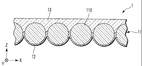
FIG. 1 is a plan view schematically showing an
optical device according to an embodiment of the
CA 02699277 2010-03-10
present invention. FIG. 2 is a sectional view taken
along the line II-II of the optical device shown in
FIG. 1.
The optical device 1 includes a particulate layer
5 11, a reflecting layer 12 and a carrier layer 13. The
optical device 1 has a front surface on the side of the
carrier layer 13 and a back surface on the side of the
reflecting layer 12.
The particulate layer 11 is made of transparent
particles 110 arranged two-dimensionally.
Specifically, the transparent particles 110 are
arranged in X direction and Y direction which are
parallel with a display surface of the optical device 1
and cross each other. Here, X direction and Y
direction form an angle of about 60 .
The transparent particles 110 are not stacked in
layers in Z direction which is perpendicular to X
direction and Y direction. That is, the particulate
layer 11 is a monolayer of the transparent particles
110.
The transparent particles 110 are arranged
regularly. Typically, the transparent particles 110
form an array structure which includes irregularities
and/or defects. Here, for the sake of simplifying an
explanation, it is supposed that the transparent
particles 110 are arranged regularly. Specifically, it
is supposed that the transparent particles 110 form a
CA 02699277 2010-03-10
6
triangle lattice.
An average particle diameter of the transparent
particles 110 is, for example, 2.5 pm or less. The
average particle diameter may fall within a range of
200 nm to 800 nm, or a range of 200 nm to 500 nm, or a
range of 200 nm to 400 nm.
A particle-size distribution, here a number
distribution, of the transparent particles 110
satisfies the following conditions, for example. That
is, 70% or more of the particles has a particle
diameter 0.8 times the average particle diameter or
more and 1.2 times the average particle diameter or
less. Typically, 90% or more of the particles has a
particle diameter 0.9 times the average particle
diameter or more and 1.1 times the average particle
diameter or less.
The transparent particles 110 may be in contact
with each other or be spaced apart from each other.
A proportion of the transparent particles 110 in a
unit area, namely, a filling factor is, for example,
30% or more, and typically 60% or more.
An average center-to-center distance of the
transparent particles 110 is equal to or longer than
the average particle diameter of the transparent
particles 110. The average center-to-center distance
of the transparent particles 110 is, for example,
2.5 pm or less. The average center-to-center distance
CA 02699277 2010-03-10
7
may fall within a range of 200 nm to 800 nm, or a range
of 200 nm to 500 nm, or a range of 200 nm to 400 nm.
An average ratio of the maximum diameter with
respect to the minimum diameter of the transparent
particles 110 falls, for example, within a range of 1.0
to 1.2. Typically, the transparent particles 110 have
roughly spherical shapes. The transparent particles
110 may have other shapes. For example, the
transparent particles 110 may have roughly spheroidal
shapes.
Here, almost all the numerical values for the
transparent particles 110 are values obtained utilizing
a scanning electron microscope (SEM) and/or a
transmission electron microscope (TEM). Specifically,
three fields of view are chosen on the particulate
layer 110 at random, and then a microphotograph is
taken for each field of view. The size of each field
of view are determined such that a sufficient numbers
of the transparent particles 110 are present therein
and size of each transparent particle 110 can be
measured accurately. For example, the size of each
field of view is set at 100 pm2 or more. Using these
microphotographs, the numerical values for the
transparent particles 110 are obtained. Note that the
average particle diameter and the particle-size
distribution of the transparent particles 110 are an
average and a number distribution of the maximum
CA 02699277 2010-03-10
8
diameters obtained for all the transparent particles
110 within each field of view, respectively. Note also
that the filling factor is a numerical value obtained
when each transparent particle 110 is supposed to be a
sphere having the same diameter as the above-described
average particle diameter.
The transparent particles 110 are made of a
colorless or colored transparent material. Typically,
the transparent particles 110 are made of a colorless
transparent material. The transparent particles 110
are made of, for example, an organic or inorganic
material.
As the organic material, for example, acrylic
resin, polyester, polyimide, polyolefin, polymethyl
acrylate, polymethyl methacrylate, polyethylene,
polypropylene, polyether sulfone, polyamide, nylon,
polyurethane, polyvinyl chloride, polyvinylidene
chloride, acrylamide, or a copolymer including one or
more of them can be used.
As the inorganic material, for example, calcium
carbonate, barium carbonate, magnesium carbonate,
calcium silicate, barium silicate, magnesium silicate,
calcium phosphate, barium phosphate, magnesium
phosphate, silicon oxide, titanium oxide, iron oxide,
cobalt oxide, zinc oxide, nickel oxide, manganese
oxide, aluminum oxide, iron hydroxide, nickel
hydroxide, aluminum hydroxide, calcium hydroxide,
CA 02699277 2010-03-10
9
chrome hydroxide, zinc hydroxide, aluminum silicate,
zinc carbonate, basic copper carbonate, zinc sulfide or
glass can be used.
Each transparent particle 110 may have a
homogeneous composition or an inhomogeneous
composition. In the latter case, the transparent
particle 110 may include, for example, a core portion
and a shell portion covering the entire surface of the
core portion and having a refractive index different
from that of the core portion. Alternatively, the
transparent particle 110 may include a plurality of
layers having different refractive indices and stacked
alternately. Alternatively, the transparent particle
110 may be subjected to a surface treatment.
The transparent particle 110 may be solid, hollow
or porous. The porous transparent particle 110 may be
an aggregate of fine particles or not.
The reflecting layer 12 covers the back surface of
the particulate layer 11. The interface between the
reflecting layer 12 and the particulate layer 11 has a
light-reflecting property.
The reflecting layer 12 may have a light-
transmitting property or a light-shielding property.
For example, in the case where it offers a
transmittance of 20% or more over the whole visible
range, for example, the wavelength range of 400 nm to
700 nm, an image behind the optical device 1 can be
CA 02699277 2010-03-10
observed therethrough.
The interface between the reflecting layer 12 and
the particulate layer 11 is provided with a first
relief structure which includes first recesses or
5 protrusions corresponding to the transparent particles.
The first relief structure emits a first diffracted
light when illuminated with a light. The light is
typically a visible light. Note that the sizes of the
first recesses or protrusions are the same as that of
10 the transparent particles 110.
As the material of the reflecting layer 12, for
example, a metal or alloy, a transparent dielectric
material, or a combination thereof can be used.
The transparent dielectric material is different
from the transparent particles, for example, in
refractive index. For example, an absolute value of
the difference between the refractive index of the
transparent dielectric material and the refractive
index of the transparent particles 110 is 0.2 or more.
When this difference is great, a high reflectance can
be achieved.
As the transparent dielectric material, ceramics
or a polymeric organic substance can be used. As the
ceramics, for example, antimony oxide (Sb203: 3.0),
ferric oxide (Fe203: 2.7), titanium oxide (Ti02: 2.6),
cadmium sulfide (CdS: 2.6), cerium oxide (Ce02: 2.3),
zinc sulfide (ZnS: 2.3), lead chloride (PbCl2: 2.3),
CA 02699277 2010-03-10
11
cadmium oxide (CdO: 2.2), antimony oxide (Sb203: 5),
tungsten oxide (W03: 5), silicon monoxide (SiO: 5),
silicon dioxide (Si02: 1.45), silicon trioxide (Si203:
2.5), indium oxide (In203: 2.0), lead oxide (PbO: 2.6),
tantalum oxide (Ta203: 2.4), zinc oxide (ZnO: 2.1),
zirconium oxide (Zr02: 5), magnesium oxide (MgO: 1),
dimeric silicon monoxide(Si202: 10), magnesium fluoride
(MgF2: 4), cerium fluoride (CeF3: 1), calcium fluoride
(CaF2: 1.3-1.4), aluminum fluoride (AlF3: 1), aluminum
oxide (A1203: 1) or gallium oxide (GaO: 2) can be used.
As the polymeric organic substance, for example,
polyethylene (1.51), polypropylene (1.49),
polytetrafluoroethylene (1.35), polymethyl methacrylate
(1.49) or polystyrene (1.60) can be used. Note that
the numerical values within the parentheses represent
refractive indices.
Alternatively, as the material of the reflecting
layer 12, a mixture of particles made of metal, alloy,
ceramics or polymeric organic substance and a
transparent resin may be used. In this case, the
reflecting layer 12 may also serve as a sticky layer or
an adhesive layer.
The reflecting layer 12 may have a monolayer
structure or a multilayer structure. In the latter
case, the reflecting layer 12 may be, for example, a
multilayer designed to cause multi-beam interference.
The reflecting layer 12 may cover the entire back
CA 02699277 2010-03-10
12
surface of the particulate layer 11. Alternatively,
the reflecting layer 12 may cover only a part of the
back surface of the particulate layer 11. That is, the
reflecting layer 12 may be patterned. In this case,
the reflecting layer 12 may be patterned in order to
define a contour of an image to be displayed on the
optical device 1. Alternatively, the reflecting layer
12 may be patterned in dots or mesh form in order to
achieve the optimum reflectance.
The carrier layer 13 covers the front surface of
the particulate layer 11. The carrier layer 13
supports the transparent particles 110. Less than half
the volume of each transparent particle 110 is embedded
in the carrier layer. The carrier layer 13 may be
omitted.
The interface between the carrier layer 13 and the
particulate layer 11 has a light-transmitting property.
This interface has a reflectance smaller than that of
the light-reflecting interface between the reflecting
layer 12 and the particulate layer 12. For example,
the light-transmitting interface has a smaller
reflectance for the light diffracted by the first
relief structure as compared with the light-reflecting
interface.
Typically, the light-transmitting interface has a
transmittance greater than that of the light-reflecting
interface between the reflecting layer 12 and the
CA 02699277 2010-03-10
13
particulate layer 11. For example, the light-
transmitting interface has a smaller transmittance for
the light diffracted by the first relief structure as
compared with the light-reflecting interface.
The interface between the carrier layer 13 and the
particulate layer 11 is provided with a second relief
structure which includes second recesses or protrusions
corresponding to the transparent particles 110. The
second relief structure emits a second diffracted light
when irradiated with a light. This light is typically
a visible light. Note that the sizes of the second
recesses or protrusions are the same as that of the
transparent particles 110.
The carrier layer 13 is made of a colorless or
colored transparent material. Typically, the carrier
layer 13 is colorless and transparent. As the material
of the carrier layer 13, for example, a transparent
resin can be used.
In the case where a volumetric ratio of the
carrier layer 13 is sufficiently small with respect to
a volumetric ratio of the particulate layer 11, for
example, in the case where an average thickness of the
carrier layer 13 is less than 50% of the average
diameter of the transparent particles 110, there is a
probability that the carrier layer 13 is localized in
the void between the transparent particles 110 or at a
point of contact between the transparent particles 110.
CA 02699277 2010-03-10
14
Alternatively, there is a probability that the front
surface of the carrier layer 13 has a shape
corresponding to the surface shape of the particulate
layer 11. In such cases, the refractive index of the
carrier layer 13 may be different from or equal to the
refractive index of the transparent particles 110.
In the case where the front surface of the carrier
layer 13 is flat, the carrier layer 13 has a refractive
index different from that of the transparent particles
110. An absolute value of the difference between the
refractive indices falls, for example, within a range
of 0.1 to 1.5.
When the optical device 1 is irradiated with light
from the front,'each of the first and second relief
structures emits a diffracted light. The diffracted
light emitted by the first relief structure and the
diffracted light emitted by the second relief structure
can cause constructive interference or destructive
interference. Further, each of the first and second
relief structures scatters part of incident light.
That is, each of the first and second relief
structures emits a diffracted light and a scattered
light. In addition, when the observation conditions
are changed, the wavelength of the diffracted light is
changed, and the intensity ratio of the diffracted
light with respect to the scattered light is also
changed.
CA 02699277 2010-03-10
An optical device 1 from which the particulate
layer 11 and the carrier layer 13 are omitted does not
emit a scattered light at high intensity. On the other
hand, an optical device 1 from which the reflecting
5 layer 12 is omitted does not emit a diffracted light at
high intensity and does not emit a scattered light at
high intensity. That is, when the structure described
with reference to FIGS. 1 and 2 is employed, a special
visual effect can be achieved.
10 In the optical device 1, the average center-to-
center distance of the transparent particles 110 may be
set sufficiently small. For example, the center-to-
center distance may be set at 500 nm or less, or 400 nm
or less. By doing so, it is possible to allow a
15 diffracted light to be observed with high visibility
only in a special situation as will be described below.
As described above, each of the first and second
relief structures serves as a diffraction grating.
When a diffraction grating is illuminated with a light,
the diffraction grating emits a diffracted light at
high intensity in a direction specific to a propagation
direction of the illumination light as incident light.
In the case where a light propagates in a plane
perpendicular to grating lines of a diffraction
grating, an angle of emergence R of mth-order
diffracted light (m=O, 1, 2, ...) can be calculated
using the following equation (1).
CA 02699277 2010-03-10
16
d = mi\/(sina-sinR) ... (1)
In this formula (1), d represents a grating
constant, m represents an order of diffraction, and X
represents a wavelength of the incident light and the
diffracted light. Further, a represents the angle of
emergence of the 0-order diffracted light, i.e., the
transmitted light or the regular reflected light. In
other words, an absolute value of a is equal to the
incident angle of the illumination light, and in the
case of a reflection-type diffraction grating, an
incident direction of the illumination light and an
emergence direction of the regular reflected light are
symmetrical to each other with respect to a normal of
the interface on which the diffraction grating is
provided.
Note that in the case where the diffraction
grating is of the reflection-type, the angle a is equal
to or greater than 0 and less than 90 . Note also
that in the case of obliquely irradiating the interface
having the diffraction grating thereon with an
illumination light and considering two angular ranges
bordering with each other at an angle of the normal
direction, i.e., 0 , the angle R has a positive value
when the emergence direction of the diffracted light
and the emergence direction of the regular reflected
light are within the same angular range. On the other
hand, the angle R has a negative value when the
CA 02699277 2010-03-10
17
emergence direction of the diffracted light and the
incident direction of the illumination light are within
the same angular range. Hereinafter, the angular range
which includes the emergence direction of the regular
reflected light is referred to as "positive angular
range", while the angular range which includes the
incident direction of the illumination light is
referred to as "negative angular range".
In the case where the diffraction grating is
observed in a normal direction thereof, the diffracted
light having an angle of emergence of 00 is the only
diffracted light that contributes to the display.
Therefore, in this case, if the grating constant d is
greater than the wavelength X, there exist a wavelength
X and an incident angle a that satisfy the above
equation (1). That is, in this case, an observer can
observe a diffracted light having a wavelength A which
satisfies the above equation (1).
By contrast, in the case where the grating
constant d is smaller than the wavelength A, there is
no incident angle a that satisfies the above
equation (1). Therefore, in this case, the observer
cannot observe a diffracted light.
As will be apparent from the above description, in
the case where the average center-to-center distance of
the transparent particles 110 is set sufficiently
small, each of the first and second relief structures
CA 02699277 2010-03-10
18
do not emit a diffracted light in the normal direction,
or alternatively, a diffracted light emitted by each of
the first and second relief structures in the normal
direction is the one whose visibility is low.
In the case where the average center-to-center
distance of the transparent particles 110 is set
sufficiently small, an optical property which is
different from that of a normal diffraction grating in
the following respects can be further obtained.
FIG. 3 is a view schematically showing a manner in
which a diffraction grating emits a first-order
diffracted light. FIG. 4 is a view schematically
showing a manner in which another diffraction grating
emits a first-order diffracted light.
In FIGS. 3 and 4, IF represents an interface on
which a diffraction grating is formed, and NL
represents a normal of the interface IF. Further, IL
represent a white illumination light composed of a
plurality of rays having different wavelengths, RL
represents a regular reflected light or 0-order
diffracted light, and DLr, DLg and DLb represent red,
green and blue-colored first-order diffracted lights as
the results of the separation of the white illumination
light IL, respectively.
In FIG. 3, the interface IF is provided with a
diffraction grating which has a grating constant
greater than the minimum wavelength of the visible
CA 02699277 2010-03-10
19
range, for example, greater than about 400 nm. On the
other hand, in FIG. 4, the interface IF is provided
with a diffraction grating which has a grating constant
smaller than the minimum wavelength of the visible
range.
As will be apparent from the above equation (1),
in the case where the grating constant d of the
diffraction grating is greater than the minimum
wavelength of the visible range, when the interface IF
is obliquely irradiated with the illumination light IL
as shown in FIG. 3, the diffraction grating emits the
first-order diffracted lights DLr, DLg and DLb at
emergence angles Rr, Rg and Rb within the positive
angular range. Although not shown in the figure, the
diffraction grating also emits first-order diffracted
lights of other wavelengths at this time.
By contrast, in the case where the grating
constant d of the diffraction grating is greater than
half the minimum wavelength of the visible range and
smaller than the minimum wavelength, the diffraction
grating emits the first-order diffracted lights DLr,
DLg and DLb at emergence angles Rr, Rg and Rb within
the negative angular range.
As will be apparent from the above description,
when the average center-to-center distance of the
transparent particles 110 is made sufficiently small,
each of the first and second relief structures does not
CA 02699277 2010-03-10
emit a diffracted light within the positive angular
range but emits a diffracted light only within the
negative angular range. Alternatively, each of the
first and second relief structures emits a diffracted
5 light within the positive angular range with low
visibility and emits a diffracted light within the
negative angular range with high visibility. That is,
different from a normal diffraction grating, each of
the first and second relief structures emits a
10 diffracted light with high visibility only within the
negative angular range.
Further, in the optical device 1, the transparent
particles 110 form recesses or protrusions having
tapered shapes on each of the light-reflecting
15 interface and the light-transmitting interface. In the
case of employing such a structure, if the center-to-
center distance is sufficiently small, each of the
interfaces and a region in the vicinity thereof can be
considered to have a refractive index continuously
20 changing in Z direction. Thus, the reflectances of the
light-reflecting interface and light-transmitting
interface are small regardless of the angle of
observation. Further, as described above, the first
and second relief structures emit substantially no
diffracted light in the normal direction. In addition,
the transparent particles 110 scatter part of the
incident light.
CA 02699277 2010-03-10
21
That is, in the case where the center-to-center
distance is sufficiently small, the optical device 1
emits almost no regular reflected light. Further in
this case, the optical device 1 emits a diffracted
light with high visibility only within the negative
range. In addition, the optical device 1 emits the
scattered light over a wide angular range.
Therefore, the optical device 1 displays a dark
muddy color when observed from the front. The optical
device 1 also displays a dark muddy color when
illuminated in a direction within the negative angular
range and observed in a direction within the positive
angular range. In addition, the optical device 1
displays a spectral color when illuminated in a
direction within the negative and observed in a
direction within the negative angular range.
As above, setting the center-to-center distance
sufficiently small allows a diffracted light with high
visibility to be observed only under a special
condition. In addition, the optical device 1 displays
a dark muddy color under other conditions. Thus, in
the case where the optical device 1 is a genuine
article, an optical device whose genuineness is unknown
can be discriminated between a genuine article and a
non-genuine article by checking the above optical
characteristics.
Although described herein is the behavior of the
CA 02699277 2010-03-10
22
light within the visible range, the same phenomenon
occurs to the light within the infrared region. That
is, when the center-to-center distance is set
appropriately, it is possible to prevent the optical
device 1 from emitting a diffracted light within the
positive angular range for any wavelength within a
specific wavelength range, for example, within a
wavelength range of 1,000 nm to 1,200 nm. Further, in
this case, it is possible to allow the optical device 1
to emit a diffracted light having a wavelength within
the above specific wavelength range in a direction
within the negative angular range. Therefore, it is
possible to discriminate an optical device whose
genuineness is unknown between a genuine article and a
non-genuine article using infrared light.
The optical device 1 achieves superior forgery
prevention effects in the other respects.
As described above, the transparent particles 110
typically form an array structure which includes
irregularities and/or defects. The same irregularities
and/or defects cannot be reproduced using the
manufacturing method described later.
Further, the array structure including
irregularities and/or defects is unique to each optical
device 1. Therefore, when the array structure is
recorded in advance, an optical device whose
genuineness is unknown can be discriminated between a
CA 02699277 2010-03-10
23
genuine article and a non-genuine article by comparing
an array structure included in the particular optical
device with the recorded array structure.
Furthermore, in each relief structure formed by
the transparent particles 110, a ratio of height of the
protrusions with respect to the center-to-center
distance of the protrusions is great. In addition, the
transparent particle 110 typically has a shape which
includes a combination of a forward tapered shape and a
reverse tapered shape. It is very difficult to
replicate such a structure by a transfer from the
optical device 1. Even if such a replication is
possible, the same visual effect as that of the optical
device 1 cannot be achieved unless the same materials
as those of the constituents of the optical device 1
are used.
As above, when the optical device 1 is used,
discrimination between a genuine and a forgery can be
performed using a plurality of methods. In addition,
the optical device 1 is very difficult to forge. Thus,
according to this technique, superior forgery
prevention effects can be achieved.
The optical device 1 can be manufactured, for
example, by the following method.
First, the carrier layer 13 is formed on a
substrate (not shown). As the substrate, for example,
a film with a smooth surface can be used. The carrier
CA 02699277 2010-03-10
24
layer 13 is formed, for example, by a printing method
such as gravure printing, micro-gravure printing,
reverse gravure printing, roll coating, bar-coat
printing, flexographic printing, screen printing, spin-
coat printing, spray-coat printing and ink-jet
printing. The carrier layer 13 is formed to have a
thickness which is, for example, smaller than the
average particle diameter of the transparent particles
110, for example, a thickness falling within a range of
0.001% to 80% of the average particle diameter of the
transparent particles 110, and typically a thickness of
about 25% of the average particle diameter of the
transparent particles 110.
In the case where the carrier layer 13 is formed
using a printing method, as the coating solution, for
example, a liquid resin or a composition containing a
resin and a solvent can be used. As the resin, for
example, sticky resin, hot-tack resin, thermoplastic
resin, thermosetting resin, ultraviolet-curing resin or
ionizing radiation-curing resin can be used. As the
solvent, for example, water or a nonaqueous solvent can
be used.
The coating solution may further contain a
crosslinker. Alternatively, the resin contained in the
coating solution may include a crosslinkable reaction
group. As the crosslinkable reaction group, for
example, isocyanate group, epoxy group, carbodiimide
CA 02699277 2010-03-10
group, oxazoline group or silanol group can be used.
For example, when the surfaces of the transparent
particles 110 are modified with the crosslinkable
reaction group, it is possible to cause a crosslinking
5 reaction between the transparent particles 110 or to
cause a crosslinking reaction between the resin and the
transparent particles 110. Not that when causing the
crosslinking reaction, the coating solution may further
contains a catalyst which promotes the reaction.
10 Instead of using the printing method for forming
the carrier layer 13, a film or sheet-like carrier
layer 13, which can be handled alone, may be used. As
the material of such a carrier layer 13, for example,
the above-described resin can be used.
15 Next, the particulate layer 11 is formed on the
carrier layer 13.
For example, the transparent particles 110 are
dispersed on the carrier layer 13, and then the
transparent particles 110 are fixed onto the carrier
20 layer 13. In the case where the carrier layer 13 is
sticky, the transparent particles 110 are fixed on the
carrier layer 13 when they are in contact with the
carrier layer 13. In the case where the carrier layer
13 is made of a hot-tack resin or thermoplastic resin,
25 the transparent particles 110 can be fixed on the
carrier layer 13, for example, by heating the carrier
layer 13 when dispersing the transparent particles 110
CA 02699277 2010-03-10
26
and cooling it thereafter. In the case where the
carrier layer 13 is made of a thermosetting resin, the
transparent particles 110 can be fixed on the carrier
layer 13 by heating the carrier layer 13 after
dispersing the transparent particles 110. In the case
where the carrier layer 13 is made of an ultraviolet-
curing resin or ionizing radiation-curing resin, the
transparent particles 110 can be fixed on the carrier
layer 13 by exposing the carrier layer 13 to an
ultraviolet radiation or ionization radiation after
dispersing the transparent particles 110. Note that
the transparent particles 110 can be fixed on the
carrier layer 13 also by removing the solvent after
dispersing the transparent particles 110.
After fixing, excess transparent particles 110 are
removed. For removing, for example, suction, blowing
or washing using liquid is utilized. Thus, the
particulate layer 11 is obtained.
Then, the reflecting layer 12 is formed on the
particulate layer 11.
The reflecting layer 12, which is made of metal,
alloy or ceramics, is formed, for example, by vapor
deposition such as vacuum evaporation, sputtering and
chemical vapor deposition. When using the vapor
deposition, the reflecting layer 12 can be formed as a
continuous film. Also, in a film-forming process using
vapor deposition, in particular, physical vapor
CA 02699277 2010-03-10
27
deposition, a deposition material such as metal or
alloy is initially deposited in an island or mesh-
pattern, and then forms a continuous film. Therefore,
when utilizing this, an island or mesh-like reflecting
layer 12 can be obtained. The island or mesh-like
reflecting layer 12 has a transmittance higher than
that of a reflecting layer as a continuous film.
The reflecting layer 12 may be formed using
oblique evaporation or oblique sputtering. When using
oblique evaporation or oblique sputtering, the
reflecting layer 12 can be obtained to have an
anisotropic reflecting property. In this case, a more
complicated visual effect can be achieved as compared
with the case where the reflecting layer 12 is formed
to have an isotropic reflecting property.
The reflecting layer 12 made of a polymeric
organic substance or the above mixture is formed, for
example, using a printing method such as gravure
printing, flexographic printing and screen printing.
In this case, the thickness of the reflecting layer 12
is set, for example, within a range of 0.001 pm to
10 pm.
Thereafter, the reflecting layer 12 is patterned
as needed. Thus, the optical device 1 is obtained.
According to this method, a microstructure can be
formed without using heat-embossing or
photolithography. Thus, according to this method, a
CA 02699277 2010-03-10
28
high productivity can be achieved.
Various modifications can be made to this
manufacturing method.
For example, the carrier layer 13 and the
particulate layer 11 may be formed simultaneously.
That is, the transparent particles 110 are contained in
the coating solution used for forming the carrier layer
13. Then, the coating solution is applied to the
substrate, and subsequently the coated film is
hardened. Thereafter, excess transparent particles 110
are removed. If the carrier layer 13 is sufficiently
thin, the particulate layer 11 can be obtained as a
monolayer of the transparent particles 110. Thus, the
carrier layer 13 and the particulate layer 11 are
formed simultaneously. Then, the reflecting layer 12
is formed on the particulate layer 11. As above, the
optical device 1 is obtained.
The optical device thus obtained is different from
the optical device 1 shown in FIG. 2 in the following
respects. This will be described with reference to
FIG. S.
FIG. 5 is a sectional view schematically showing a
modified example of the optical device shown in FIGS. 1
and 2.
The optical device 1 shown in FIG. 5 further
includes a substrate 14 and a transparent cover layer
15.
CA 02699277 2010-03-10
29
The substrate 14 faces the particulate layer 11
with the carrier layer 13 interposed therebetween. The
substrate 14 can be omitted.
The transparent cover layer 15 is interposed
between the particulate layer 11 and the reflecting
layer 12. The transparent cover layer 15 is made of
the same material as that of the carrier layer 13.
When the back surface of the particulate layer 11
is covered with the transparent cover layer 15 as
above, the transparent particles 110 are less prone to
fall off.
The optical device 1 shown in FIG. 5 can be formed
by other methods. For example, the carrier layer 13
and the particulate layer 11 are formed on the
substrate 14 in this order, and subsequently the
transparent cover layer 15 is formed on the particulate
layer 11. Then, the reflecting layer 12 is formed on
the transparent cover layer 15 so as to obtain the
optical device 1 shown in FIG. 5. Note that in the
case of employing this method, the material of the
transparent cover layer 15 may be the same as or
different from the material of the carrier layer 13.
Other modifications can be made to this optical
device 1.
FIG. 6 is a sectional view schematically showing
another modified example of the optical device shown in
FIGS. 1 and 2.
CA 02699277 2010-03-10
The optical device 1 shown in FIG. 6 is the same
as the optical device 1 described with reference to
FIGS. 1 and 2 except that the transparent particles 110
form a square lattice. As above, the transparent
5 particles 110 may form a lattice other than the
triangular lattice.
FIG. 7 is a sectional view schematically showing
still another modified example of the optical device
shown in FIGS. 1 and 2.
10 The optical device 1 shown in FIG. 7 is the same
as the optical device 1 described with reference to
FIGS. 1 and 2 except that the following structure is
employed. That is, this optical device 1 further
includes the substrate 14. In addition, the
15 particulate layer 11 includes regions lla to 11c.
The regions lla to llc are different from one
another in the particle diameters of the transparent
particles 110. Thus, the regions 11a to lIc are
different from one another in the center-to-center
20 distances of the transparent particles 110. Therefore,
the portions of the optical device 1 corresponding to
the regions 11a to llc do not emit diffracted lights in
the same direction or alternatively emits diffracted
lights having different wavelengths in the same
25 direction.
In the case of employing such a structure, a
multicolored image can be displayed on the optical
CA 02699277 2010-03-10
31
device 1. That is, a more complicated image can be
displayed on the optical device 1.
FIG. 8 is a sectional view schematically showing
still another modified example of the optical device
shown in FIGS. 1 and 2.
The optical device 1 shown in FIG. 8 is the same
as the optical device 1 described with reference to
FIGS. 1 and 2 except that the following structure is
employed. That is, this optical device 1 further
includes the substrate 14 and a polarizer 16.
The polarizer 16 faces the particulate layer 11
with the substrate 16 and the carrier layer 13
interposed therebetween. The polarizer 16 is, for
example, a linear polarizer.
As the polarizer 16, for example, a polarizing
film prepared by drawing a resin film added with a
dichromatic dye can be used.
Alternatively, as the polarizer 16, the polarizing
layer obtained by the following method may be used.
First, a coated film made of polyimide, polyamide or
polyvinyl alcohol is formed using spin coating and then
dried. Next, the coated film is subjected to rubbing
process or photo-alignment process to obtain an
alignment layer. Thereafter, a dichromatic dye or a
composition containing a dichromatic dye and a nematic
liquid crystal material is applied to the alignment
layer, and then the coated film is dried. The
CA 02699277 2010-03-10
32
polarizing layer thus obtained may be used as the
polarizer 16.
The polarizer 16 may be adhered on the substrate
16. Alternatively, the polarizer 16 may be formed on
the substrate 16.
When the structure shown in FIG. 8 is employed,
the visual effect described below can be obtained.
Note that for the sake of simplification, it is
supposed here that the transparent particles 110 form
the square lattice shown in FIG. 6, and one of the
array directions thereof is parallel with X direction.
Further, it is supposed that the polarizer 16 is a
linear polarizer having a transmission axis parallel
with X direction.
In the case where a grating constant d of a
diffraction grating, and a wavelength A and an
incidence angle 0 of an incident light satisfy the
relationship represented by the following inequality
(2), the diffraction structure behaves on an
s-polarized light as if it is a thin film having an
effective refractive index NTM-
dxcos6<X ... (2)
Note that an s-polarized light is a linearly
polarized light in which a vibration direction of the
electric field vector is perpendicular to the
propagation directions of the illumination light and
the diffracted light, i.e., TE wave (transverse
CA 02699277 2010-03-10
33
electric wave). On the other hand, a p-polarized light
is a linearly polarized light which has a vibration
direction of the electric field vector different from
that of the s-polarized light by 90 , i.e., TM wave
(transverse magnetic wave).
Except for the case where the depth of the groove
of the diffraction grating differs from the grating
constant d, an effective refractive index NTE and an
effective refractive index NTT are different from each
other. In the case where the incident angle 0
satisfies the relationship represented by the following
inequality (3) or (4), an s-polarized light enters the
above-described thin film, while a p-polarized light
cannot enter the thin film but is reflected by this
thin film. Note that in the following inequalities (3)
and (4), Nl is a refractive index of a medium located
in front of the above-described thin film.
NTM/N1<sinA<NTE/N1 ... (3)
NTE/N1<sin6<NTM/N1 ... (4)
As will be apparent from the above, in the case
where the incident angle A satisfies the relationship
represented by the in equality (3) or (4), the
diffracted lights emitted by the first and second
relief structures are s-polarized lights or p-polarized
lights. Here, as an example, it is supposed that when
the incident angle 0 satisfies the relationship
represented by the in equality (3) or (4), the first
CA 02699277 2010-03-10
34
and second relief structures emit s-polarized lights as
the diffracted lights.
As described above, the transmission axis of the
polarizer 16 is parallel with X direction. Therefore,
in the case where the optical device 1 is illuminated
in a direction perpendicular to X direction at an
incident angle 0 that satisfies the relationship
represented by the inequality (3) or (4), the
diffracted lights are transmitted by the polarizer 16.
On the other hand, in the case where the optical device
1 is illuminated in a direction perpendicular to Y
direction at an incident angle 0 that satisfies the
relationship represented by the inequality (3) or (4),
the diffracted lights are absorbed by the polarizer 16.
Thus, when rotating the optical device 1 around an axis
parallel with Z direction while the illumination
direction and the observation angle kept unchanged, the
optical device 1 displays a bright image and a dark
image alternately.
In the case of using the polarizer 16, the
structure shown in FIG. 9 or 10 may be employed in the
optical device 1.
FIG. 9 is a sectional view schematically showing a
modified example of the optical device shown in FIG. 8.
The optical device 1 shown in FIG. 9 is the same
as the optical device 1 described with reference to
FIG. 8 except that the polarizer is patterned.
CA 02699277 2010-03-10
For example, it is supposed that a first portion
of the optical device 1 corresponding to the opening of
the polarizer 16 emits an s-polarized light as a
diffracted light. In this case, when the vibration
5 direction of the electric field vector of the
s-polarized light is parallel with the transmission
axis of the polarizer 16, a second portion of the
optical device 1 corresponding to the polarizer 16 also
emits a diffracted light. By contrast, when the
10 vibration direction of the electric field vector of the
s-polarized light is perpendicular to the transmission
axis of the polarizer 16, the second portion does not
emit a diffracted light.
That is, under a certain observation condition,
15 both the first and second portions can be seen bright.
On the other hand, under another observation condition,
the first portion can be seen bright, while the second
portion can be seen dark.
FIG. 10 is a sectional view schematically showing
20 another modified example of the optical device shown in
FIG. 8.
The optical device 1 shown in FIG. 10 is the same
as the optical device 1 described with reference to
FIG. 8 except that the particulate layer 11 is
25 patterned.
A third portion of the optical device 1
corresponding to the opening of the particulate layer
CA 02699277 2010-03-10
36
11 does not emit a diffracted light but emit a regular
reflected light. On the other hand, a fourth portion
of the optical device 1 corresponding to the
particulate layer 1 behaves as the above-described
second portion.
The structures shown in FIGS. 9 and 10 can be
combined with each other. That is, the optical device
1 may includes two or more of the following portions: a
portion in which both the particulate layer 11 and the
polarizer 16 are provided, a portion in which either
one of the particulate layer 11 and the polarizer 16 is
provided, and a portion in which neither the
particulate layer 11 nor the polarizer is provided.
The visual effects described with reference to
FIGS. 1 and 2 can be obtained when the following
structure is employed.
FIG. 11 is a plan view schematically showing an
optical device according to another embodiment of the
present invention.
The optical device 1 shown in FIG. 11 includes a
front layer 13', a back layer 17, a reflecting layer 12
and an interlayer 11'. The optical device 1 has a
front surface on the side of the front layer 13' and a
back surface on the side of the back layer 17.
The front layer 13' is a colorless or colored
transparent layer. Typically, the front layer 13' is
colorless and transparent.
CA 02699277 2010-03-10
37
The front layer 13' is made of, for example,
resin. As the material of the front layer 13', for
example, photo-setting resin, thermosetting resin or
thermoplastic resin can be used.
The main surface of the front layer 13 that facing
the back layer 17 is provided with the above-described
first relief structure. The front layer 13' plays
almost the same optical role as that of the carrier
layer 13. Therefore, the optical properties required
for the front layer 13' are almost the same as the
optical properties required for the carrier layer 13.
The back layer 17 faces the front layer 13'. The
main surface of the back layer 17 that faces the front
layer 13' is provided with a third relief structure
which is almost the same as the above-described second
relief structure. In the case of observing in Z
direction, the recesses included in the second relief
structure are arranged at the same positions as that of
the recesses included in the first relief structure.
The back 'layer 17 is made of, for example, resin.
As the material of the back layer 17, for example,
photo-setting resin, thermosetting resin or
thermoplastic resin can be used.
The reflecting layer 12 cover the main surface of
the back layer 17 that is provided with the relief
structure. The surface of the reflecting layer 12
facing the front layer 13' is provided with the
CA 02699277 2010-03-10
38
above-described second relief structure.
The interlayer 11' is interposed between the front
layer 13' and the reflecting layer 12. The interlayer
11' is a colorless or colored transparent layer.
Typically, the interlayer 11' is colorless and
transparent.
The interlayer 11' is made of, for example, resin.
As the material of the interlayer 11', for example,
photo-setting resin, thermosetting resin or
thermoplastic resin can be used.
The interface between the interlayer 11' and the
front layer 13' corresponds to the above-described
light-transmitting interface. On the other hand, the
interface between the interlayer 11' and the reflecting
layer 12 corresponds to the above-described light-
reflecting interface. That is, the interlayer 11'
plays almost the same optical role as that of the
particulate layer 11. Therefore, the optical
properties required for the interlayer 11' are almost
the same as the optical properties required for the
particulate layer 11.
The optical device 1 can be manufactured, for
example, by the following method.
First, a thermoplastic resin or photo-setting
resin is applied to a substrate (not shown), and then
the resin is cured while pushing a master against the
coated film. The master is provided with a relief
CA 02699277 2010-03-10
39
structure which corresponds to the third relief
structure. Thus, the back layer 17 is obtained.
Next, the reflecting layer 12 is formed on the
back layer 17 using vapor deposition. The reflecting
layer 17 is formed such that it covers the third relief
structure.
Thereafter, the front layer 13' is obtained by the
same method as that described for the back layer 17.
Then, an adhesive or pressure-sensitive adhesive
is applied to the front layer 13' and/or the reflecting
layer 12. Subsequently, the front layer 13' and the
back layer 17 are bonded together such that the
reflecting layer 12 and the adhesive or pressure-
sensitive adhesive are interposed therebetween.
Thereafter, the adhesive is cured as needed.
Thus, the optical device 1 shown in FIG. 11 is
completed.
The optical device 11 shown in FIG. 11 can be
manufactured by another method.
First, by the same method as described above, the
back layer 17 and the reflecting layer 12 are formed in
this order.
Next, a thermoplastic resin or photo-setting resin
is applied to the reflecting layer 12, and then the
resin is cured while pushing a master against the
coated film. The master is provided with a relief
structure which corresponds to the first relief
CA 02699277 2010-03-10
structure. Thus, the interlayer 11' is obtained.
Then, the front layer 13' is formed on the
interlayer 11'. The front layer 13' is obtained, for
example, by applying a resin to the interlayer 11' and
5 then hardening the resin layer.
Thus, the optical device 1 shown in FIG. 11 is
completed. Note that in this method, the stacking
order may be reversed. That is, the front layer 13',
the interlayer 11', the reflecting layer 12 and the
10 back layer 17 may be formed in this order.
The optical device 1 shown in FIG. 11 can be
manufactured by still another method.
First, using two masters, formed is an interlayer
11' in which a main surface thereof is provided with
15 the first relief structure, while the other main
surface thereof is provide with the second relief
structure. For example, a thermoplastic resin or
photo-setting resin is applied to one of the masters,
and the resin is cured while pressing the other master
20 against the coated film.
Next, the front layer 13' is formed on one of the
main surfaces of the interlayer 11', while the
reflecting layer and the back layer 17 are formed on
the other main surface of the interlayer 11' in this
25 order. The front layer 13' is obtained, for example,
by applying a resin to the interlayer 11' and then
hardening the resin layer. The reflecting layer 12 is
CA 02699277 2010-03-10
41
firmed, for example, using vapor deposition. The back
layer 17 is obtained, for example, by applying a resin
to the reflecting layer 12 and then hardening the resin
layer.
Thus, the optical device 1 shown in FIG. 11 is
completed.
Various modifications can be made to the optical
device 1.
For example, one of the front layer 13' and the
back layer 17 may be omitted. Alternatively, both the
front layer 13' and the back layer 17 may be omitted.
It is possible that the main surface of the front
electrode provided with the first relief structure does
not face the reflecting layer 12. That is, the first
relief structure may be provided on the front surface
of the front layer 13'.
It is also possible that the main surface of the
back layer 17 provided with the third relief structure
does not face the front layer 13'. That is, the third
relief structure may be provided on the back surface of
the back layer 17. Note that in this case, the
reflecting layer 12 should be formed to cover the back
surface of the back layer 17.
In the case where the first relief structure is
provided on the front surface of the front layer 13',
the interlayer 11' may be omitted. Similarly, in the
case where the third relief structure is provided on
CA 02699277 2010-03-10
42
the back surface of the back layer 17, the interlayer
11' may be omitted.
The structure described with reference to FIGS. 1
to 10 may be employed in this optical device 1. For
example, the reflecting layer 12 may be a continuous
film or be patterned.
It is possible that when observed in Z direction,
the recesses included in the second relief structure do
not arranged at the same positions as those of the
recesses included in the first relief structure. For
example, the bottoms of the recesses included in the
second relief structure may face the boundaries between
the recesses included in the first relief structure.
The center-to-center distance of the recesses or
protrusions included in the first relief structure may
be different from the center-to-center distance of the
recesses or protrusions included in the second relief
structure.
FIG. 12 is a sectional view schematically showing
a modified example of the optical device shown in
FIG. 11. FIG. 13 is a sectional view schematically
showing another modified example of the optical device
shown in FIG. 11.
In the optical device 1 shown in FIG. 11, the
center-to-center distance of the recesses or
protrusions included in the first relief structure is
smaller than the center-to-center distance of the
CA 02699277 2010-03-10
43
recesses or protrusions included in the second relief
structure.
By contrast, in the optical device 1 shown in
FIG. 12, the center-to-center distance of the recesses
or protrusions included in the first relief structure
is greater than the center-to-center distance of the
recesses or protrusions included in the second relief
structure.
When employing the structure shown in FIG. 12 or
13, the first and second relief structures behave as
diffraction gratings having different grating
constants. In addition, in the case where the
structure shown in FIG. 12 or 13 is employed, it is
possible to achieve a light-scattering property which
is different from that achieved in the case of
employing the structure shown in FIG. 11. Thus, when
the structure shown in FIG. 12 or 13 is employed, it is
possible to achieve visual effects which are different
from those achieved in the case of employing the
structure shown in FIG. 11.
The optical device 1 described with reference to
FIGS. 1 to 13 may further include a printed layer on
the front surface or between layers. The printed layer
may be a continuous film or be patterned. Note that in
the case of disposing the printed layer as a continuous
film in front of the light-reflecting interface, a
transparent material should be used as the material of
CA 02699277 2010-03-10
44
the printed layer.
The optical device 1 may further include an
overcoat as an uppermost layer. When the overcoat is
provided, the uppermost surface of the optical device 1
can be made substantially flat.
In the manufacturing process of the optical device
1, corona discharge treatment, plasma treatment or
flame treatment may be performed. When such a
treatment is performed, a high interlaminer strength
can be achieved.
The optical device 1 may further include a light-
absorbing layer disposed at the back of the light-
reflecting interface. The light-absorbing layer is,
for example, a black layer or a colored layer which
reflects a colored light when illuminated with a white
light. When the light-absorbing layer is provided, if
the reflecting layer 12 ahs a high transmittance or the
reflecting layer 12 is patterned, it is possible, for
example, to allow the light-absorbing layer to absorb
the light transmitted by the reflecting layer 12 or the
opening thereof.
The optical device 1 may further include an
interface which regularly reflects an incident light at
a high reflectance. Alternatively, the optical device
1 may further include a light-scattering structure
which scatters an incident light. Alternatively, the
optical device 1 may further include both the interface
CA 02699277 2010-03-10
which regularly reflects an incident light at a high
reflectance and the light-scattering structure which
scatters an incident light.
The optical device 1 described with reference to
5 FIGS. 1 to 13 can be used, for example, for the purpose
of forgery prevention. The optical device 1 may be
used for other purposes other than forgery prevention.
For example, the optical device 1 may be used as a toy,
a learning material, an ornament, etc.
10 The optical device 1 can be utilized in various
forms as will be described below.
FIG. 14 is a sectional view schematically showing
an example of a laminate which includes an optical
device.
15 The laminate 2a shown in FIG. 14 is a transfer
foil. The transfer foil 2a includes an optical device
1 and a support layer 21a.
The optical device 1 is the same as the optical
device 1 described with reference to FIGS. 1 and 2
20 except for employing the following structure.
That is, the optical device 1 further includes an
adhesive layer 18a and a protective release layer 19.
The adhesive layer 18a covers the back surface of
the reflecting layer. The adhesive layer 18a is made
25 of, for example, thermoplastic resin. For example, in
the case where a thermoplastic resin layer is formed on
a surface of an article prior to the transfer, the
CA 02699277 2010-03-10
46
adhesive layer 18a may be omitted.
The protective release layer 19 is interposed
between the support layer 21a and the carrier layer 13.
The protective release layer 19 is provided in order to
promote peeling of the optical device 1 from the
support layer 21a. The protective release layer 19
also serves as a protective film which protects the
carrier layer 13 from damage.
As the material of the protective release layer
19, for example, a mixture of polymethyl methacrylate
resin and another thermoplastic resin such as vinyl
chloride-vinyl acetate copolymer or nitrocellulose
resin, or a mixture of polymethyl methacrylate resin
and polyethylene wax can be used. Alternatively, as
the protective release layer 19, it is possible to use
a layer obtained by forming a coated film made of a
mixture of cellulose acetate resin and thermosetting
resin such as epoxy resin, phenol resin, thermosetting
acrylic resin or melamine resin, and then thermosetting
the coated film.
The protective release layer 19 may be omitted.
Alternatively, instead of the protective release layer
19, a release layer may be interposed between the
support layer 21a and the carrier layer 13.
The release layer is a layer for promoting the
peeling of the optical device 1 from the support layer
21a. Different from the protective release layer 19,
CA 02699277 2010-03-10
47
the release layer remains on the support layer 21a when
the optical device 1 is peeled off from the support
layer 21a. As the material of the release layer, for
example, silicone resin or fluorocarbon resin can be
used.
The support layer 21a releasably supports the
front surface of the optical device 1. The support
layer 21a has a sufficient strength against the heat,
pressure, etc. applied on the transfer. As the support
layer 21a, for example, a polyethylene terephthalate
(PET) layer, polyethylene naphthalate layer or
polyimide layer can be used. In the case of
transferring the optical device 1 onto a surface having
a three-dimensional structure, it is possible to use as
the support layer 21a a layer which becomes soft by
heating. As such a layer, for example, a polyethylene
layer, polypropylene layer, vinyl chloride layer or
amorphous PET layer can be used.
FIG. 15 is a sectional view schematically showing
another example of a laminate which includes an optical
device.
The laminate 2b shown in FIG. 15 is a peel-off
label. The transfer foil 2a includes a optical device
1 and a support layer 21b.
The optical device 1 is the same as that described
with reference to FIGS. 1 and 2 except for employing
the following structure. That is, the optical device 1
CA 02699277 2010-03-10
48
is an adhesive label which further includes the
substrate 13 and a pressure-sensitive adhesive layer
18b. The pressure-sensitive adhesive layer 18b is made
of a pressure-sensitive adhesive. The pressure-
sensitive adhesive layer 18b covers the back surface of
the reflecting layer 12.
The optical device 1 may be provided with a notch
or perforation so that it causes brittle fracture when
it is fraudulently peeled off from an article. The
optical device 1 may also include a part where the
interlaminer strength is low.
The support layer 21b releasably supports the back
surface of the optical device 1. The support layer 21a
is, for example, a release paper.
The transfer foil 2a and the peel-off label 2b can
be used, for example, in manufacturing a labeled
article. Note that the optical devices 1 of the
transfer foil 2a and the peel-off label 2b can be
modified, for example, as described with reference to
FIGS. 1 to 13.
FIG. 16 is a plane view schematically showing an
example of a labeled article. FIG. 17 is a sectional
view taken along the line XVII-XVII of the labeled
article shown in FIG. 16.
The labeled article 3 includes the optical device
1 described with reference to FIGS. 1 to 13 and an
article 31.
CA 02699277 2010-03-10
49
The article 31 is an article whose genuineness is
to be verified. The article 31 is, for example, an
authentication medium such as cash card, credit card
and passport, or a marketable security medium such as
gift certificate and stock certificate. Typically, the
article 31 is a printed matter. The article 31 may be
an article other than the authentication medium and
marketable security. For example, the article 31 may
be a craft product or an art object. Alternatively,
the article 31 is a package including a packaging
material and an object contained therein.
In the case where the article 31 is a printed
matter, as the material of the article 31, for example,
a resin superior in a heat-resisting property can be
used. As such a resin, for example, polyethylene
naphthalate, polyimide, polyethylene, polypropylene or
vinyl chloride can be used.
The optical device 1 is supported by the article
31. For example, the optical device 1 is adhered to
the article 510. In this case, the optical device 1
can be supported by the article 31, for example, using
the transfer foil 2a shown in FIG. 14 or the peel-off
label 2b shown in FIG. 15.
Instead of using the adhesive layer 18a or the
pressure-sensitive adhesive 18b for making the optical
device 1 supported by the article, it may be supported
by the article using other methods.
CA 02699277 2010-03-10
Note that in the labeled article 3, the optical
device 1 further includes a printed layer. The printed
layer may be a continuous layer or be patterned. The
optical device 1 shown in FIG. 16 includes a printed
5 pattern which displays a character string "Security".
FIG. 18 is a plane view schematically showing
another example of a labeled article.
The labeled article 4 includes a paper 41 and the
optical device 1 embedded in the paper 41. The labeled
10 article 4 can be obtained, for example, by sandwiching
the optical device 1 between layers of fibers during
paper making, and then performing printing onto the
paper surface, etc., as needed. Note that in order to
make it easy to visually recognize the image displayed
15 on the optical device 1, an opening may be provided at
the portion of the paper that covers the front surface
of the optical device. There is no limitation on the
shape of the optical device 1 embedded in the paper.
For example, a thread or strip-shaped optical device 1
20 may be embedded in the paper.
The optical device 1 may be used in the form of
ink.
FIG. 19 is a sectional view schematically showing
an example of an ink. In FIG. 19, the reference symbol
25 6 indicates a container containing ink 5.
The ink 5 includes a liquid binder resin 51 and
the optical devices 1. The optical devices 1 have been
CA 02699277 2010-03-10
51
broken into pieces and are dispersed in the binder
resin. As the binder resin, for example, a printing
binder or vehicle can be used.
The printed pattern obtained using this ink 5
includes the optical devices 1. Therefore, this
printed pattern offers the above visual effect that
described for the optical device 1.
In the case where the optical devices 1, which
have been broken into pieces, are used, there is a
possibility that some of the optical devices face the
back side of the article. In the case where the
optical devices 1, which have been broken into pieces,
are used, two optical devices 1 may be bonded together
such that their back sides face each other as will be
described below.
FIG. 20 is a sectional view schematically showing
an optical device according to still another embodiment
of the present invention.
The optical device 1 has a structure in which a
front portion and a back portion are bonded together
via an interlayer 18.
The interlayer 18 is made of an adhesive or
pressure-sensitive adhesive.
Each of the front and back portions are the same
as the optical device 1 described with reference to
FIGS. 1 and 2 except for further including the
substrate 14. The front and back portions are bonded
CA 02699277 2010-03-10
52
together such that their reflecting layers 12 face each
other.
Both surfaces of the optical device 1 are display
surfaces. Therefore, in the case where such optical
devices 1, which have been broken into pieces, are
used, the display surfaces of almost all the optical
devices 1 face the front side of the labeled article.
Examples of the present invention will be
described below.
<Example 1>
An acrylic resin was applied to a PET film with a
thickness of 25 pm using bar-coating. As the acrylic
resin, used was BMW6110 manufactured by TOYO INK MFG.
CO., LTD. The coated film was formed to have a
thickness of 0.2 pm after drying.
The coated film was heated in an oven set at 120 C
for 3 minutes, and then dispersed on the coated film
was spherical transparent particles having diameters of
about 300 nm and made of polystyrene. As the
transparent particles, 3300B manufactured by MORITEX
CORP. was used. Spray coating was used for dispersing
the transparent particles. 90% or more of the
transparent particles had particle diameters 0.8 times
or more and 1.2 times or less of the average particle
diameter.
The coated film on which the transparent particles
were dispersed was further heated in the oven set at
CA 02699277 2010-03-10
53
120 C for 30 seconds, and then the transparent
particles not fixed on the coated film were removed
using a vacuum cleaner. The transparent particles
remained on the coated film formed a monolayer having a
filling factor of 50% or more.
Thereafter, an aluminum layer with a thickness of
80 nm was formed on the particulate layer using vacuum
evaporation. Thus, an optical device was obtained.
Note that the front surface of this optical device is a
surface of the PET film.
The optical device was observed from the front
while illuminating its front surface with a white
light. In this case, the optical device displayed a
dark red-purple image regardless of the illumination
direction.
Then, the optical device was observed in a
direction within the negative angular range while
obliquely illuminating its front surface with the white
light. In the case where the observation angle
was -45 or less, the optical display displayed an
image which had colors ranging from blue to green due
to diffracted lights. Note that 80% or more of the
diffracted lights were TE polarized light, i.e.,
s-polarized light.
Next, a polarizing film was adhered on the
aluminum layer of the optical device via an acrylic
pressure-sensitive adhesive such that the polarizing
CA 02699277 2010-03-10
54
film covers only a part of the aluminum layer. Thus,
an optical device including a polarizer was obtained.
The optical device was observed from the front
while illuminating its front surface with a white
light. In this case, a first portion of the optical
device in which the polarizing film was not adhered
displayed a dark red-purple image. On the other hand,
a second portion of the optical device in which the
polarizing film was adhered displayed a dark red-purple
image. Although the image displayed on the second
portion had a color darker than that displayed on the
first portion, it was difficult to discriminate them
from each other.
Then, the optical device was observed in a
direction within the negative angular range while
illuminating its front surface with the white light.
In the case where the observation angle was -45 or
less, the first portion displayed an image which had
colors ranging from blue to green due to diffracted
lights. On the other hand, the second portion
displayed an image darker than that displayed on the
first portion. Further, the optical device was rotated
around its normal while the illumination direction and
the observation direction were kept unchanged. As a
result, the difference in brightness between the first
and second portions was changed in accordance with the
rotation of the optical device.
CA 02699277 2010-03-10
<Example 2>
Prepared was a fluid dispersion containing a
solution of polyvinyl alcohol and spherical transparent
particles having diameters of about 300 nm and made of
5 polystyrene. As the solution of polyvinyl alcohol,
PVAHC manufactured by KURARAY CO., LTD. was used. As
the transparent particles, 3300B manufactured by
MORITEX CORP. was used. A mass ratio of polyvinyl
alcohol with respect to the spherical particles was
10 1/20.
Then, the fluid dispersion was applied to a PET
film with a thickness of 25 pm using bar-coating. The
coated film was heated in an oven set at 120 C for
3 minutes, and then excess transparent particles were
15 removed using a vacuum cleaner. The transparent
particles remained on the coated film formed a
monolayer having a filling factor of 50% or more.
Thereafter, an aluminum layer with a thickness of
80 nm was formed on the particulate layer using vacuum
20 evaporation. Thus, an optical device was obtained.
Note that the front surface of this optical device is a
surface of the PET film.
The optical device was observed from the front
while illuminating its front surface with a white
25 light. In this case, the optical device displayed a
dark green image regardless of the illumination
direction.
CA 02699277 2010-03-10
56
Then, the optical device was observed in a
direction within the negative angular range while
obliquely illuminating its front surface with the white
light. In the case where the observation angle
was -45 or less, the optical display displayed an
image which had colors ranging from blue to green due
to diffracted lights. Note that 80% or more of the
diffracted lights were TE polarized light, i.e.,
s-polarized light.
Next, polyimide was applied to the aluminum layer
of the optical device. The coated film was dried and
then subjected to rubbing processing to obtain an
alignment layer. Specifically, a part of the coated
film and another part of the coated film were rubbed in
different directions. A rayon cloth was used for the
rubbing processing.
Then, prepared was a composition containing a
dichromatic dye and a polymerizable nematic liquid
crystal material. The composition was prepared such
that low transmittances were achieved over the visible
range. The composition was applied to the alignment
layer, and subsequently the coated film was hardened to
obtain a polarizing layer.
Thus, an optical device was obtained. Note that
the front surface of the optical device is the surface
of the polarizing layer.
The optical device was observed from the front
CA 02699277 2010-03-10
57
while illuminating its front surface with a white
light. In this case, it was impossible to discriminate
the two portions of the optical device having different
rubbing directions from each other.
Then, the optical device was observed in a
direction within the negative angular range while
obliquely illuminating its front surface with the white
light. In the case where the observation angle
was -45 or less, the two portions of the optical
device having different rubbing directions were seen to
be different from each other in brightness. Further,
the optical device was rotated around its normal while
the illumination direction and the observation
direction were kept unchanged. As a result, the bright
and dark images changed their places between the two
portions.
<Example 3>
An optical device including a polarizer was
manufactured by the same method as described in Example
1 except that transparent particles with diameters of
about 150 nm were used.
The optical device was observed in a direction
within the negative angular range while obliquely
illuminating its front surface with the white light and
rotating the optical device around its normal.
However, almost no change was caused in the difference
in brightness between the first and second portions
CA 02699277 2010-03-10
58
<Example 4>
An acrylic resin was applied to a PET film with a
thickness of 25 pm using bar-coating. As the acrylic
resin, used was BMW6110 manufactured by TOYO INK MFG.
CO., LTD. The coated film was formed to have a
thickness of 0.2 pm after drying.
The coated film was heated in an oven set at 80 C
for 1 minute, and then dispersed on the coated film was
spherical transparent particles having diameters of
about 500 nm and made of polystyrene. As the
transparent particles, 3500B manufactured by MORITEX
CORP. was used. Spray coating was used for dispersing
the transparent particles. 90% or more of the
transparent particles had particle diameters 0.8 times
or more and 1.2 times or less of the average particle
diameter.
The coated film on which the transparent particles
were dispersed was further heated in the oven set at
80 C for 1 minute, and then the transparent particles
not fixed on the coated film were removed using a
vacuum cleaner. The transparent particles remained on
the coated film formed a monolayer having a filling
factor of 50% or more.
Thereafter, an aluminum layer with a thickness of
80 nm was formed on the particulate layer using vacuum
evaporation. Thus, an optical device was obtained.
Note that the front surface of this optical device is a
CA 02699277 2010-03-10
59
surface of the PET film.
The optical device was observed from the front
while illuminating its front surface with a white
light. In this case, the optical device displayed a
dark blue-green image regardless of the illumination
direction.
Then, the optical device was observed in a
direction within the negative angular range while
obliquely illuminating its front surface with the white
light. In the case where the observation angle was
less than -30 , the optical display displayed an image
which had colors ranging from blue to red due to
diffracted lights.
<Example 5>
Prepared was a fluid dispersion containing a
solution of polyvinyl alcohol and spherical transparent
particles having diameters of about 500 nm and made of
polystyrene. As the solution of polyvinyl alcohol,
PVAHC manufactured by KURARAY CO., LTD. was used. As
the transparent particles, 3500B manufactured by
MORITEX CORP. was used. A mass ratio of polyvinyl
alcohol with respect to the spherical particles was
1/20.
Then, the fluid dispersion was applied to a PET
film with a thickness of 25 pm using bar-coating. The
coated film was heated in an oven set at 80 C for
1 minute, and then excess transparent particles were
CA 02699277 2010-03-10
removed using a vacuum cleaner. The transparent
particles remained on the coated film formed a
monolayer having a filling factor of 50% or more.
Thereafter, an aluminum layer with a thickness of
5 80 nm was formed on the particulate layer using vacuum
evaporation. Thus, an optical device was obtained.
Note that the front surface of this optical device is a
surface of the PET film.
The optical device was observed from the front
10 while illuminating its front surface with a white
light. In this case, the optical device displayed a
dark blue-green image regardless of the illumination
direction.
Then, the optical device was observed in a
15 direction within the negative angular range while
obliquely illuminating its front surface with the white
light. In the case where the observation angle was
less than -30 , the optical display displayed an image
which had colors ranging from blue to red due to
20 diffracted lights.
<Example 6>
Prepared was a fluid dispersion containing a
solution of polyvinyl alcohol and spherical transparent
particles having diameters of about 300 nm and made of
25 polystyrene. As the solution of polyvinyl alcohol,
PVAHC manufactured by KURARAY CO., LTD. was used. As
the transparent particles, 3300B manufactured by
CA 02699277 2010-03-10
61
MORITEX CORP. was used. A mass ratio of polyvinyl
alcohol with respect to the spherical particles was
1/20.
Then, the fluid dispersion was applied to a PET
film with a thickness of 25 pm using bar-coating. The
coated film was heated in an oven set at 80 C for
1 minute, and then excess transparent particles were
removed using a vacuum cleaner. The transparent
particles remained on the coated film formed a
monolayer having a filling factor of 50% or more.
Thereafter, an aluminum layer with a thickness of
80 nm was formed on the particulate layer using vacuum
evaporation. Thus, an optical device was obtained.
Note that the front surface of this optical device is a
surface of the PET film.
The optical device was observed from the front
while illuminating its front surface with a white
light. In this case, the optical device displayed a
dark purple-blue image regardless of the illumination
direction.
Then, the optical device was observed in a
direction within the negative angular range while
obliquely illuminating its front surface with the white
light. In the case where the observation angle was
less than -45 , the optical display displayed an image
which had colors ranging from blue to green due to
diffracted lights.
CA 02699277 2010-03-10
62
<Example 7>
Prepared was a fluid dispersion containing a
solution of polyvinyl alcohol and spherical transparent
particles having diameters of about 500 nm and made of
polystyrene. As the solution of polyvinyl alcohol,
PVAHC manufactured by KURARAY CO., LTD. was used. As
the transparent particles, 3500B manufactured by
MORITEX CORP. was used. A mass ratio of polyvinyl
alcohol with respect to the spherical particles was
1/20.
Then, the fluid dispersion was applied to a PET
film with a thickness of 25 um using bar-coating. The
coated film was heated in an oven set at 80 C for
1 minute, and then excess transparent particles were
removed using a vacuum cleaner. The transparent
particles remained on the coated film formed a
monolayer having a filling factor of 50% or more.
Thereafter, a titanium oxide layer with a
thickness of 50 nm was formed on the particulate layer
using vacuum evaporation. Thus, a transparent optical
device was obtained. Note that the front surface of
this optical device is a surface of the PET film.
The optical device was observed from the front
while illuminating its front surface with a white
light. In this case, the optical device displayed a
dark blue-green image regardless of the illumination
direction.
CA 02699277 2010-03-10
63
Then, the optical device was observed in a
direction within the negative angular range while
obliquely illuminating its front surface with the white
light. In the case where the observation angle was
less than -30 , the optical display displayed an image
which had colors ranging from blue to red due to
diffracted lights.
<Example 8>
Prepared was a fluid dispersion containing a
solution of polyvinyl alcohol, first transparent
particles having diameters of about 200 nm, second
transparent particles having diameters of about 300 nm,
and third transparent particles having diameters of
about 400 nm. The mass ratio of polyvinyl alcohol, the
first transparent particles, the second transparent
particles, and the third transparent particles was
1:5:10:5. As the solution of polyvinyl alcohol, PVAHC
manufactured by KURARAY CO., LTD. was used. As the
first transparent particles, 3200B manufactured by
MORITEX CORP. was used. As the second transparent
particles, 3300B manufactured by MORITEX CORP. was
used. As the third transparent particles, 3400B
manufactured by MORITEX CORP. was used. The first to
third particles are spherical particles made of
polystyrene.
Note that the average particle diameter of the
transparent particles contained in the fluid dispersion
CA 02699277 2010-03-10
64
was about 300 nm. Note also that 50% of the
transparent particles had particle diameters 0.8 times
or more and 1.2 times or less of the average particle
diameter.
Then, the fluid dispersion was applied to a PET
film with a thickness of 25 pm using bar-coating. The
coated film was heated in an oven set at 80 C for
1 minute, and then excess transparent particles were
removed using a vacuum cleaner. The transparent
particles remained on the coated film formed a
monolayer having a filling factor of 50% or more.
Thereafter, an aluminum layer with a thickness of
80 nm was formed on the particulate layer using vacuum
evaporation. Thus, an optical device was obtained.
Note that the front surface of this optical device is a
surface of the PET film.
The optical device was observed in the normal and
oblique directions while illuminating its front surface
with a white light. As a result, the optical display
displayed a gray image regardless of the illumination
and observation direction.
<Example 9>
A solution of polyvinyl alcohol was mixed with
spherical transparent particles having diameters of
about 300 nm and made of polystyrene such that a mass
ratio of polyvinyl alcohol with respect to the
spherical particles was 1/20. As the solution of
CA 02699277 2010-03-10
polyvinyl alcohol, PVAHC manufactured by KURARAY CO.,
LTD. was used. As the transparent particles, 3300B
manufactured by MORITEX CORP. was used. The mixed
solution was diluted with distilled water at a 4-fold
5 dilution factor to obtain a fluid dispersion.
Then, the fluid dispersion was applied to a PET
film with a thickness of 25 um using bar-coating. The
coated film was heated in an oven set at 80 C for
1 minute, and then excess transparent particles were
10 removed using a vacuum cleaner. The transparent
particles remained on the coated film formed a
monolayer having a filling factor of 25%.
Thereafter, an aluminum layer with a thickness of
80 nm was formed on the particulate layer using vacuum
15 evaporation. Thus, an optical device was obtained.
Note that the front surface of this optical device is a
surface of the PET film.
The optical device was observed in the normal and
oblique directions while illuminating its front surface
20 with a white light. As a result, the optical display
displayed a gray image regardless of the illumination
and observation direction.
<Example 10>
Prepared was a fluid dispersion containing a
25 solution of polyvinyl alcohol and spherical transparent
particles having diameters of about 500 nm and made of
polystyrene. As the solution of polyvinyl alcohol,
CA 02699277 2010-03-10
66
PVAHC manufactured by KURARAY CO., LTD. was used. As
the transparent particles, 3500B manufactured by
MORITEX CORP. was used. A mass ratio of polyvinyl
alcohol with respect to the spherical particles was
1/20.
Then, the fluid dispersion was applied to a PET
film with a thickness of 25 pm using bar-coating. The
coated film was heated in an oven set at 80 C for
1 minute, and then excess transparent particles were
removed using a vacuum cleaner. The transparent
particles remained on the coated film formed a
monolayer having a filling factor of 50% or more.
Thereafter, an aluminum layer with a thickness of
50 nm was formed on the particulate layer using vacuum
evaporation. Thus, an optical device was obtained.
Note that the front surface of this optical device is a
surface of the PET film.
The spectral transmission characteristics of the
optical device were determined. As a result, the
optical device had transmittances of about 15% over the
whole wavelength range of 400 nm to 700 nm.
The optical device was adhered to a printed patter
via an acrylic pressure-sensitive adhesive such that
the back surface of the optical device faced the front
surface of the printed matter. Note that no printed
pattern of the printed patter could be seen through the
optical device.
CA 02699277 2010-03-10
67
Next, the optical device was observed from the
front while illuminating its front surface with a white
light. In this case, the optical device displayed a
dark blue-green image regardless of the illumination
direction.
Then, the optical device was observed in a
direction within the negative angular range while
obliquely illuminating its front surface with the white
light. In the case where the observation angle was
less than -30 , the optical display displayed an image
which had colors ranging from blue to red due to
diffracted lights.
Additional advantages and modifications will
readily occur to those skilled in the art. Therefore,
the invention in its broader aspects is not limited to
the specific details and representative embodiments
shown and described herein. Accordingly, various
modifications may be made without departing from the
spirit or scope of the general inventive concept as
defined by the appended claims and their equivalents.