Note: Descriptions are shown in the official language in which they were submitted.
CA 02699698 2010-03-17
WO 2009/036567 PCT/CA2008/001652
EVANESCENT FIELD OPTICAL FIBER DEVICES
FIELD OF THE INVENTION
The present invention relates to evanescent field optical fiber devices,
including optical
fiber sensors.
BACKGROUND OF THE INVENTION
Evanescence based fiber optic sensors have received considerable attention in
the past
years due to their widespread applications in various parameter measurements
such as
temperatures, pressures and of biological and chemical materials that may be
present in
an environment or sample of interest.
Various techniques, well known in the art, have been developed to access the
evanescent
field in an optical fiber. For example, an optical fiber may be tapered by
stretching it
while it is heated, e.g. over a flame. Another technique is by polished
coupler in a glass
block to protect the optical fiber during the grinding and polishing steps. A
third
technique entails removal of a portion of the cladding by mechanical or
chemical means.
However, when a portion of the cladding of an optical fiber is removed to
access the
evanescent field, the fiber already of minute diameter is increasingly more
fragile and
delicate. Although the third technique may be carried out in very specialized
circumstances such as in a laboratory, it is very difficult to manufacture and
difficult to
use.
Therefore, there is a need for improved techniques for use of optical fibers
as components
of optical sensors and such sensors that have good mechanical resistance and,
of course,
that are easy to use and to manufacture. Such a need also exists for improved
techniques
for use of optical fibers in components of systems using optical fibers, such
as optical
fiber communications systems, including couplers, splitters, repeaters,
switchers,
amplifiers, attenuators, isolators and the like.
1
CA 02699698 2010-03-17
WO 2009/036567 PCT/CA2008/001652
One approach for optical sensors is described in U.S. patent application
2004/0179765 in
which an optical fiber is coupled or connected to a larger optical waveguide
in which a
portion of the cladding, and optionally the core, has been removed using any
suitable
known techniques in the art, to pennit access to the evanescent field.
However, to be put
into practice, this type of sensing device requires an alignment or axial
coupling of two or
more optical fibers with a separate optical waveguide of far larger diameter.
This step is
not only complex but also requires very precise alignment in order to minimize
the loss
of light energy.
Thus, it is desired to improve on evanescence based fiber optic sensors,
having a good
mechanical resistance with improved durability and ease of assembly and use.
SUMMARY OF THE INVENTION
The present invention reduces the difficulties and the disadvantages of the
prior art by
reinforcing an optical fiber itself without, for example, the need of
connecting the latter to
another optical waveguide.
The present invention relates to an evanescent field optical fiber device
comprising one
or more optical fibers wherein a portion of said one or more fibers is without
coating, and
a support which provides for the mechanical integrity of the one or more
optical fiber and
for access of the evanescent field without impairing the optical fiber.
More particularly, the present invention provides an evanescence based optical
fiber
device comprising one or more optical fibers as above and a support which
assures
mechanical strength of the optical fiber wherein one or more grooves has been
machined
in the support and in a cladding portion of the one or more optical fibers in
order to gain
access to the evanescent field.
2
CA 02699698 2010-03-17
WO 2009/036567 PCT/CA2008/001652
In a further embodiment, the present invention relates to the use of a support
in the
mechanical or chemical removal of cladding from an optical fiber for use in an
evanescence based fiber optic device.
Another embodiment is the method of using the support for the mechanical or
chemical
removal of cladding from an optical fiber for use in an evanescence based
fiber optic
device.
A further embodiment of the present invention is such a support for one or
more optical
fibers or such optical devices, comprised of shape memory material.
BRIEF DESCRIPTION OF THE DRAWINGS
In order that the invention may be more readily understood, currently
preferred
embodiments will now be further described by way of example with reference to
the
accompanying drawings in which:
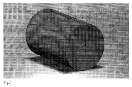
Figure 1 is an isometric view of the support of the present invention;
Figure 2 is an isometric view of an evanescent field optical fiber sensor that
has an
optical fiber, a support and a groove machined in the support and in a
cladding portion of
the optical fiber;
Figure 3 is a side view of an evanescent field optical fiber sensor that has
an optical fiber,
a support and a groove machined in the support and in a cladding portion of
the optical;
Figure 4 is an isometric view of an evanescent field optical fiber sensor that
has an
optical fiber, a support and a groove machined in the support and in a
cladding portion of
the optical fiber and wherein the groove is an axial groove;
3
CA 02699698 2010-03-17
WO 2009/036567 PCT/CA2008/001652
Figure 5 is an isometric view of the evanescent field optical fiber sensor
that has an
optical fiber, a support and a groove machined in the support and in a
cladding portion of
the optical fiber and wherein a thin layer of substrate has been applied on
the exposed
cladding portion;
Figure 6 is an isometric view of the evanescent field optical fiber sensor
that has an
optical fiber, a support and a groove machined in the support and in a
cladding portion of
the optical fiber and wherein thin layers of metal and substrate have been
applied on the
exposed cladding portion;
Figure 7 is an isometric view of an evanescent field optical fiber sensor that
includes a
responsive layer between two exposed cladding portions of the evanescent field
optical
fiber sensors of the present invention;
Figure 8 is a cross-sectional view of Figure 7;
Figure 9 is a top plan view of the evanescent field optical fiber sensor
comprising two
optical fibers in one support and a plasmonic guide;
Figure 10 is a side view of Figure 9;
Figure 11 is a side view of Figure 9;
Figure 12 is a side view of an evanescent field optical fiber sensor based on
reflection
design;
Figure 13 is s side view of an evanescent field optical fiber sensor based on
transmission
design;
Figure 14. is a side view of an evanescent field optical fiber sensor based on
reflection
design with Bragg grating; and
4
PCT/CA2008/001652
CA 02699698 2010-03-17 16 July 2009 16-07-2009
Figure 15 is a side view of 3 evanescent field optical fiber sensors with
Bragg grating
branched in series.
DETAILED DESCRIPTION OF THE INVENTION
The present invention is based on a particular use of devices as a support for
optical
fibers in optical fiber devices, such as optical fiber sensors, couplers,
splitters, repeaters,
switchers, amplifiers, attenuators, isolators and the like. Such devices are
of the type as
described in U.S. Patent Nos. 7,066,656 and 7,121,731, and WO 2005/040876
published
May 6, 2005. A skilled person would understand that the optical fiber will
generally comprises at least one core, a cladding and a protective coating
layer. For
simplicity, we refer herein to cladding only, but it will be understood that
when
discussing the removal of cladding for the purpose of practicing the present
invention,
this will include the removal of any other coating on an optical fiber, as may
be
necessary.
The present invention is herein described in more detail in an embodiment
relating to
optical fiber sensors, although a skilled person will readily appreciate and
be able to put
into practice other embodiments of the invention as described herein and based
on the
following teachings.
Referring to Fig. 1, the connector has a longitudinally extending body which
may be
generally cylindrical. Consequently, for the purpose of this invention, this
connector will
be named a support. Indeed, although the support is shown here as cylindrical,
it may be
of any shape which is suitable for such a support. The body of the support has
a first end
and a second end. The body has a fiber conduit extending from the first end to
the second
end. The fiber conduit which is shown here as round may be of any shape
suitable for
insertion of optical fibers. Further, the support may have a plurality of
fiber conduits
depending on the number of optical fibers to insert. The diameter of the fiber
conduit is
AMENDED SHEET
PCT/CA2008/001652
CA 02699698 2010-03-17 16 July 2009 16-07-2009
slightly smaller than the sized of the optical fiber. 'fhc fiber conduit of
the support is used
to embrace an optical fiber in order to protect and to provide an adequate
mechanical
resistance to the optical fiber that permit access to the evanescent field
without impairing
the integrity of the optical fiber. In one embodiment, the support of the
present invention
has at least one longitudinal slot extending from the first end to the second
end and from
the surface of the support to the fiber conduit to allow the expansion of the
fiber conduit
for insertion of an optical fiber. However, it will be understood that the
support can be of
any suitable design for retention of an optical fiber in the conduit and can
be of the kind
of design as, for example, shown in the aforementioned U.S. Patent Nos.
7,066,656 and
7,121,731, and WO 2005/040876 published May 6, 2005. Of course, a skilled
person in the art will appreciate an be able to carry out any necessary
mechanical
modifications as may be necessary to the devices as described above for better
use as a
support as defined herein.
The support of the present invention may be made of any of several materials
depending
on its use and on the particular environment in which the support is used. For
example,
the support of the present invention may be made from a shape memory material.
For the
purposes of the present application, with respect to shape memory material
(SMM),
reference may be made to AFNOR Standard "Alliages a m6more de former -
Vocabulaire et Mesures" A 51080-1990.
Materials, which are suitable for the support of the present invention, will
illustrate a very
low Young's modulus (elastic modulus) and / or pseudo elastic effect. Pseudo
elastic
effect is encountered in SMM. Concerning the shape memory effect, when the
material is
below a temperature (MF), which is a property dependent on the particular SMM,
it is
possible to strain (deform) the material from about some tenths of a percent
to more than
about eight percent, depending on the particular SMM used. When the SMM is
heated
above a second temperature (AF), which is also dependent on the particular SMM
as well
as the applied stress, the SMM will tend to recover its assigned shape. If
unstresses, the
SMM will tend toward total recovery of its original shape. If a stress is
maintained, the
6
AMENDED SHEET
PCT/CA2008/001652
CA 02699698 2010-03-17 16 July 2009 16-07-2009
SMM will tend to particularly recover its original shape. Concerning the
pseudo elastic
effect, when the SMM is at a temperature greater than its (AF), it may be
strained at
particularly higher rates, that is exhibiting non-used elasticity, arising
from the shape
MEMORY properties. Initially, in the SMM when stressed the strain will
increase
linearly, as in a used elastic material. However, at an amount of stress,
which is
dependent on the particular SMM and temperature, the ratio of strain to stress
is no
longer linear, strain increases at a higher rate as stress is increasing at a
lower rate. At a
particular higher level of stress, the increase in strain will tend to become
smaller. This
non-linear effect exhibited by SMM a temperature above (AF) may manifest
itself as a
hysteresis like effect, wherein on the release or reduction of stress the
reduction in strain
will follow a different curve from the one manifest as stress was increased,
in the manner
of a hysteresis like loop.
An example of such above material would be a shape memory alloy (SMA).
Examples
conceming activation of the shape memory element in a SMA include D.E. Muntges
et
al., "Proceedings of SPIE", Volune 4327 (2001), pages 193-200 and Byong-Ho
Park et
al., "Proceedings of SPIE", Volume 4327 (2001), pages 79-87. Miniaturized
components
of SMA may be manufactured by laser radiation processing. See for example, H.
Hafer
Kamp et al., "Laser Zentrum Hannover e.v.", Hannover, Germany [publication).
The support of the present invention may, for example, be made from a
polymeric
material such as isostatic polybutene, shape ceramics such as zirconium with
some
addition of Cerium, Beryllium or Molybdenum, copper alloys including binary
and
ternary alloys, such as Copper - Aluminum alloys, Copper - Zinc alloys, Copper
-
Aluminum - Beryllium alloys, Copper - Aluminum - Zinc alloys and Copper -
Aluminum - Nickel alloys, Nickel alloys such as Nickel - Titanium alloys and
Nickel -
Titanium - Cobalt alloys, Iron alloys such as Iron - Manganese alloys, Iron -
Manganese
- Silicon alloys, Iron - Chromium - Manganese alloys and Iron - Chromium -
Silicon
alloys, Aluminum alloys, and high elasticity composites which may optionally
have
metallic or polymeric reinforcement.
7
AMENDED SHEET
PCT/CA2008/001652
7i CA 02699698 2010-03-17 16 July 2009 16-07-2009
In use, the fiber conduit is enlarged by deforming the support of the present
invention in
any suitable way. Without limitation, an optical fiber may be inserted into
and positioned
in the support in any manner as described in the aforementioned U.S. Patent
Nos.
7,066,656 and 7,121,731, and WO 2005/040876 published May 6, 2005, for the
purpose of practicing the present invcntion. For example and generally, a
constraint is
applied to the support which will induce an expansion of the fiber conduit for
insertion of
an optical fiber. Removal of the constraint will allow retention of the
optical fiber within
the fiber conduit of the support which then applies a uniform radial pressure
along the
fiber. At this stage, a portion of the cladding of the optical fiber can be
safely removed
for accessing the evanescent field by any known techniques in the art as, for
example,
mechanically or by chemical means, the mechanical resistance of the optical
fiber being
now adequately secured.
There are several manners to use the support of the present invention in
relation with an
optical fiber in order to have access to the evanescent field, for use an
evanescent field
optical sensor and for the making of such evanescent field optical sensor. For
example, as
shown in Figs 2 and 3, it is possible to machine, by any suitable techniques
known in the
art, a groove in the support before or after the insertion of an optical
fiber. If the groove
in the support is machined before insertion of an optical fiber, then, the
optical fiber will
be further machined using any suitable techniques known in the art by
accessing the
cladding of the optical fiber within the groove of the support. It will be
further understood
that a portion of the cladding can be removed by any other known means
including by
chemical means. It will be appreciated that the present invention does not
require removal
of all of the thickness of the cladding from a portion of the fiber. In
practice, only a
portion of the thickness of the cladding may be removed and only a part of it
retained in
the exposed portion. Moreover, the groove may also be formed axially as shown
in Fig.
4.
8
AMENDED SHEET
CA 02699698 2010-03-17
WO 2009/036567 PCT/CA2008/001652
Furthermore, in order to obtain a high-quality sensor, the portion removed
froin the
cladding of the optical fiber maintained by the support may be further
polished by any
suitable techniques known in the art as, for example, by the use of a C02
laser as
described in Nowak (Nowak, K. M. (2006).
After polishing the exposed cladding portion of the optical fiber, it is
possible to apply a
substrate in a manner known in the art on the polished surface of the optical
fiber which
shows a substantial variation of its refractive index in relation with the
parameter to
measure (temperature, pressure, shear, concentration of a particular chemical,
presence
and concentration of an agent, etc). This is well demonstrated in Fig. 5. For
example,
with respect to a temperature sensor, the elected substrate will have to
present a large
thermal dilation for a given range of temperatures to measure. This density
variation will
cause a change of the refractive index which will modify the measured signal.
The
analysis of this signal will allow to measure precisely the studied parameter.
In order to increase the absorption of the substrate and improve the precision
of the
sensor, one could add a thin layer of metal (few nanometers of thickness) over
the
polished surface of the exposed cladding before applying the substrate. This
is clearly
shown in Figure 6. The energy transmitted in the optical fiber is coupled
within the thin
layer of metal and propagates under the form of a wave called surface plasmon.
The
energy coupling between the optical fiber and the fine layer of metal strongly
depends on
the refractive index of the substrate covering the layer of metal. Therefore,
by using a
substrate having a refractive index which strongly varies with a parameter to
measure, we
can increase the sensor performances.
In a further aspect of this invention illustrated in Figures 7 and 8, other
designs of an
evanescent field optical fiber sensor are possible notably by coupling two
optical fibers of
the present invention having both exposed cladding portions. For example, one
could use
two sensors as the ones presented in Figs. 2 or 3 and inserts a responsive
layer of coating
between the two evanescent field optical fiber sensors. Then, we can quantify
any desired
parameter by measuring the transferred energy between the optical fibers I and
2.
9
CA 02699698 2010-03-17
WO 2009/036567 PCT/CA2008/001652
Referring now to Fig. 8, the substrate between the two evanescent field
optical fiber
sensors is illustrated in black. This substrate is specifically chosen to
present a variation
of its refractive index in relation with the parameter to measure. The
variation in its
refractive index will inducc variation in the spatial distribution of the
evanescent field.
Moreover, the variation of the density of the substrate will induce variation
in the
thickness d of the substrate which will modify the distance D between the core
I and the
core 2. The coupling coefficient between the two optical fibers and the signal
transferred
from the guide I to the guide 2 are thus affected. The measure and the
analysis of the
signal transmitted from the optical fiber 2 allow the determination of the
value of the
studied parameter.
Furthermore, one would understand that it is possible to apply the same
principle as
described above to an optical fiber having a multitude of cores. For example,
if an optical
fiber has two cores, the dilation and the modification of the refractive index
of the
substrate would alter the coupling between the four cores.
In a further embodiment illustrates in Figs. 9 to 11, is proposed coupling of
two optical
fibers by the addition of a plasmonic guide. In this embodiment, two optical
fibers are
inserted within a same support, the extremities of the optical fibers not
touching each
other. The addition of a thin layer of metal and a substrate between the
extremities of the
two fibers, as illustrated, will allow absorption of the energy of the first
optical fiber by
the plasmonic guide and the coupling of this energy towards the second optical
fiber. In
choosing a substrate that responds with the parameter being studied, the
analysis of this
coupling will allow the quantification of the studied parameters.
Turning now to Figs. 12 and 13, there are shown further embodiments with
respect to
evanescence based optical fiber sensor design. More partieularly, Figs. 12 and
13
represent the evanescence based optical fiber sensor design of the present
invention
relying on reflection or transmission, respectively.
CA 02699698 2010-03-17
WO 2009/036567 PCT/CA2008/001652
Firstly, for the design based on reflection (Fig. 12), the cxcitation signal
arrives by an
optical fiber, passes through the evanescence based optical fiber sensor, is
reflected when
reaching the interface fiber-air, comes back by the sensor and the fiber to be
further
analyzed. The excitation signal must be separated from the analysis signal.
This could be
done by any known techniques in the art such as, for example, the insertion of
a
separation cube.
Secondly, regarding the design based on transmission, it is possible to
connect several
evanescent field optical fiber sensors in series along a single optical fiber
to obtain
different infonmation from each of the sensors.
Moreover, the addition of Bragg grating within the fiber before and after the
active zone
allows a significant augmentation of the sensitivity of the device in order to
obtain usable
values. The Bragg grating reflects particular wavelengths of light and
transmits all others.
This is clearly illustrated in Figs. 14 and 15 which show a design in
reflection and a
desgn in transmission.
Polychromatic light travels within an optical fiber as an excitation signal.
The variation in
absorption of the evanescent wave is generated by the variation of the studied
parameter.
This absorption strongly depends from the excitation signal wavelenght, i.e.
the detection
of a certain parameter is related to a specific wavelenght while the detection
of another
parameter requires another wavelength. The Bragg grating allows the desired
wavelength
to be reflected according to the Bragg conditions while allowing the other
wavelenght to
continue as transmitted in the fiber including to other sensors. The value of
interest to be
measured by each individual sensor is captured and recovered by analysis of
the
wavelenght corresponding to the value associate with a particular sensor.
In a further embodiment, a device such as shown in Fig. 6 can be used for the
polarization of the light which travels within an optical fiber in absorbing
all the energy
which is in a polarization state. The application of an active control of the
refractive
11
CA 02699698 2010-03-17
WO 2009/036567 PCT/CA2008/001652
index by a specific manner would allow the active control of the polarization
which
travels within an optical fiber.
Furthermore, in order to rapidly and easilly control the transmitted power
within an
optical fiber, it would be appreciated that the device of the present
application could also
be used as an attenuator in order to attenuate ths signal travelling within
the fiber.
Similarly, it could also be used as a commutator.
It will be understood by the skilled person, that number of the grooves, the
dimension and
sizing of the grooves and the spatial orientation and the spacing between the
grooves
from each other can all be accomplished by known mechanical or chemical means.
The
skilled person would know how to select the appropriate components (optical
fibers,
substrate, Bragg grating, wavelength, support material, etc) for the purpose
of putting the
present invention into practice as described herein.
It will also be appreciate that these types of evanescence based optical fiber
sensors
comprising of a support with optical fiber all as described herein can be
fabricated to
have utility in extreme conditions such as a harsh fluid stream or under other
harsh
physical conditions, for example in measurement of fractional streams in
petroleum or
chemical processing; ore extractions; aeronautic and aerospace applications
and military
applications including in detection of dangerous chemical and biological
agents.
Further, it will be appreciated from the above description that the present
invention may
include all kinds of optical fibers devices such as couplers, splitters,
repeaters, switchers,
amplifiers, attenuators, isolators and the like.
While the above description constitutes the preferred embodiments, it will be
appreciated
that the present invention is susceptible to modification and change without
departing
from the fair meaning of the accompanying claims.
12