Note: Descriptions are shown in the official language in which they were submitted.
CA 02699935 2010-04-13
Digital camera and method for
testing the function of a digital camera
Motion sensors, for example motions sensors for door opening, of the prior art
mostly work with
Doppler-Radar. In other words, when an object or person approaches the sensor,
a radar beam
emitted from the sensor will be reflected by the object or person and the
reflected beam will
expierence a frequency shift (Doppler-Effect). The reflected radiation will be
recognized by the
motion sensor. However, objects which move very slowly cannot be detected due
to too low or
non-existent Doppler-Effect.
Using a camera in motion sensors provides better results, especially when
slowly moving or still
objects should be detected. However, cameras can fail due to defects in their
recognition system.
It is therefore an object of the present invention to provide a digital camera
which can be easily
and reliably tested as to its proper function.
It is also an object of the present invention to provide a test method for
testing the function of a
digital camera which may be part of a motion sensor device.
The above-mentioned objects are achieved by a digital camera and a method as
claimed in the
independent claims.
Advantageous embodiments are the subject matter of the dependent claims.
According to particular advantageous embodiments the digital camera comprises
a processor
device which is adapted to read out signals from the sensing element and
analyses whether the
read out signals correspond correctly to the electromagnetic radiation which
is irradiated onto the
sensing element by the radiation source. The radiation source, which may be a
light source, may
comprise several light elements, such as LEDs, which can be controlled
individually. The light
1
CA 02699935 2010-04-13
elements may be selected to emit different wavelengths and/or different
intensities. Also an
on/off-modulation may be provided.
For better understanding of the objects and features of the present invention
a preferred
embodiment will be described in greater detail with reference to the
accompanying drawing:
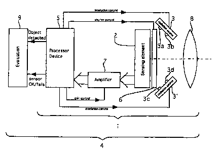
The drawing shows schematically a motion sensor device which includes a
digital video camera
I according to the invention. The digital video camera 1 comprises a sensing
element 2 which
has a square array or matrix of pixels. In front of the sensing element 2
there is shutter 6 which
can be opened or closed. In the open status of the shutter light can travel
from the camera lens 8
to the sensing element 2. In the closed status of the shutter the light
passage from the camera lens
8 to the shutter 6 is obstructed, i.e. no light from outside the camera can
fall onto the sensing
element 2. The digital video camera I further comprises a processor device 5
which receives data
from the sensing element 2. An amplifier 7 with variable gain is provided
which receives' the
pixel data from the sensing element 2 and outputs the data to the processor
device 5. The
processor device 5 is connected to an evaluation station 9. The processor
device 5 is also
connected to the gain control input of the amplifier 7. Further, the processor
device 5 is
connected to the trigger input of the shutter 6.
Radiation sources 3, 3' are provided between the optical camera lens 8 and the
shutter 6. Each of
the radiation sources 3, 3' comprises radiation elements 3a, 3b and 3c, 3d,
respectively. In this
example the radiation elements are light emitting diodes (LED). The radiation
sources 3, 3' are
arranged in such a manner that - when the shutter 6 is open - the radiation
from the radiation
elements 3a, 3b, 3c and 3d falls on the light sensitive face of the sensing
element 2. The radiation
sources 3, 3' are connected to the processing device 5 in such a manner that
each radiation
element 3a, 3b, 3c, 3d can be controlled individually by the processor device
5. Consequently,
each radiation element 3a, 3b, 3c, 3d can be switched ON or OFF and can be
dimmed
independently from the other radiation elements 3a, 3b, 3c, 3d.
2
CA 02699935 2010-04-13
In the test phase a radiation source 3 sends out its light onto the sensing
element directly, i.e. not
through the lens 8 of the camera 1. While in the latter case only a small
fraction of the matrix
would be irradiated, the light will illuminate the whole sensing element 2
when the radiation
source 3 is placed inside the camera 1 housing next to the sensing element 2.
In the following different test setup variations will be discussed:
1) Light applied to the camera sensing element 2 can test the whole sensing
element 2 or parts of
it.
a. The sensing element 2 shall be tested for safety reasons. This means that
the whole picture
field or parts of the field shall detect any object within the field. To
ensure this function the
requirement is that the pixels in the specified field shall respond to the
applied light.
b. When the response from the pixel is detected, the signal passes through the
camera processing
and the gP processing. Dependent of the signal processing the whole sensing
element 2 or part of
the sensing element 2 is included in the test.
2) Variation of shutter time in camera used in 1) can test the whole sensing
element 2 or parts of
the sensing element 2.
a. The camera can be tested as in 1). If light is applied on the camera
sensing element 2 a change
in the shutter time will change the response of each pixel in the camera.
3) Variation of gain in camera used in 1) can test the whole sensing element 2
or parts of the
sensing element 2.
a. The camera can be tested as in 1). If light is applied on the camera chip a
change in the gain
will change the response of each pixel in the camera.
3
CA 02699935 2010-04-13
4) Light applied to the edge of the camera chip used in 1) can test the whole
sensing element 2 or
parts of the sensing element 2.
a. The camera can be tested as in 1). In this situation the light is applied
from the edge of the
camera chip.
5) On/off modulation of light used in 4) can test the whole sensing element 2
or parts of the
sensing element 2.
a. When the light is applied as in 4) turning the light source on and off can
vary the applied
intensity.
6) Characteristic variation of the light intensity over the camera chip used
in 5), can test the
whole sensing element 2 or parts of the sensing element 2.
a. When the light is applied from the edge of the camera chip as in 5), the
intensity will be high
close to the light source and weak in a distance from the light source. This
gives a characteristic
variation of the light intensity over the camera chip.
b. The characteristic intensity variation can test if some addressing failure
is present when the
camera chip is read. In some cases addressing failures can result in the same
readout from to
different pixels despite the light intensity on the two pixels are different.
In this case the failure
can be revealed.
7) Light from a specified number of light sources used in 6) can test the
whole sensing element 2
or parts of the sensing element 2.
a. To ensure revealing of any addressing failure different light sources as in
6) can be combined.
This gives light combinations, which are unique for each pixel.
4
CA 02699935 2010-04-13
8) Light from specified positions of light sources used in 7) can test the
whole sensing element 2
or parts of the sensing element 2.
a. To strengthen uniqueness of the light intensity in 7) positions of the
light sources can be
specified.
9) Light sources with different wavelengths used in a given combination and a
given time
multiplexing used in 8) can test the whole sensor or parts of the sensing
element 2.
a. To strengthen uniqueness of the light intensity in 8) different wavelength
can be used. To
separate the wavelength the light sources shall be sequentially turned on and
off (Time
multiplexing). This will increase the possibility for revealing addressing
failures in a colour-
sensing camera.
5