Note: Descriptions are shown in the official language in which they were submitted.
CA 02700147 2015-05-20
CRYSTALLINE CHROMIUM ALLOY DEPOSIT
CROSS-REFERENCE TO RELATED APPLICATION
The present application is related to and claims benefit of U.S. Provisional
Application 60/976,805, filed 02 October 2007.
TECHNICAL FIELD
The present invention relates generally to electrodeposited TEM crystalline
chromium alloy deposited from trivalent chromium baths, methods and baths for
electrodepositing such chromium alloy deposits and articles having such
chromium
alloy deposits applied thereto.
BACKGROUND
Chromium electroplating began in the late 19th or early 20th century and
provides
a superior functional surface coating with respect to both wear and corrosion
resistance. However, in the past, this superior coating, as a functional
coating (as
opposed to a decorative coating), has only been obtained from hexavalent
chromium
electroplating baths. Chromium electrodeposited from hexavalent chromium baths
is
deposited in a crystalline form, which is highly desirable. Amorphous forms of
chromium plate are not useful for functional applications. The chemistry used
in the
conventional technology is based on hexavalent chromium ions, which are
considered
carcinogenic and known to be toxic. Hexavalent chromium plating operations are
subject to strict and severe environmental limitations. While industry has
developed
many methods of working with hexavalent chromium to reduce the hazards, both
industry and academia have for many years searched for a suitable alternative.
The
most often sought alternative has been trivalent chromium. Until the present
inventor's
recent successes, the efforts to obtain a dependable, reliable functional
chromium
deposit based on a trivalent chromium process has continued without success
for over
one hundred years. Additional discussion of the need for a replacement for
hexavalent
chromium is included in the earlier application related to the present
assignee's efforts
in the area of chromium deposits from trivalent chromium, published as WO
2007/115030.
1
CA 02700147 2010-03-18
WO 2009/046181
PCT/US2008/078561
As is apparent from the plethora of prior art attempts to obtain a functional
crystalline chromium deposit from trivalent chromium, there has long been
ample
motivation to seek this goal. However, as is equally apparent, this goal has
been
elusive and, prior to the present invention, has not been attained in the
prior art, despite
quite literally a hundred years of trying.
For all these reasons, a long-felt need has remained unmet for (1) a
crystalline-
as-deposited functional chromium deposit, (2) an electrodeposition bath and
process
capable of forming such a functional chromium deposit, and (3) articles made
with such
a functional chromium deposit, in which the crystalline chromium deposit is
free of
macrocracks and is capable of providing the desired functional wear and
corrosion
resistance characteristics comparable to the conventional functional hard
chromium
deposit obtained from a hexavalent chromium electrodeposition process. The
urgent
need for a bath and process capable of providing a crystalline functional
chromium
deposit from a bath substantially free of hexavalent chromium heretofore has
not been
satisfied prior to the present invention and the present inventor's previous
efforts as
disclosed in WO 2007/115030.
SUMMARY
The present inventors have discovered and developed a process and bath for
electrodepositing a nanogranular crystalline functional chromium alloy deposit
from a
trivalent chromium bath, substantially free of hexavalent chromium, in which
the deposit
obtained matches or exceeds the performance properties of a chromium deposit
obtained from a hexavalent chromium process and bath. The alloy comprises
chromium, carbon, nitrogen, oxygen and sulfur.
In one embodiment, the present invention relates to an electrodeposited
crystalline functional chromium alloy deposit, in which the deposit is
nanogranular as
deposited. In one embodiment, the deposit is both TEM and XRD crystalline, as
deposited. In another embodiment, the deposit is TEM crystalline and is XRD
amorphous.
In any of the embodiments of the present invention, the deposit may include
one
or any combination of two or more of (a) a {111} preferred orientation; (b) an
average
crystal grain cross-sectional area of less than about 500 nm2; and (c) a
lattice
parameter of 2.8895 +/- 0.0025 A.
2
CA 02700147 2010-03-18
WO 2009/046181
PCT/US2008/078561
In any of the foregoing embodiments of the invention, the deposit may include
from about 0.05 wt.% to about 20 wt.% sulfur. The deposit may include
nitrogen, in an
amount from about 0.1 to about 5 wt% nitrogen. The deposit may include carbon,
in an
amount of carbon less than that amount which renders the chromium deposit
amorphous. In one embodiment, the deposit may include from about 0.07 wt.% to
about 1.4 wt.% sulfur, from about 0.1 wt.% to about 3 wt.% nitrogen, and from
about 0.1
wt.% to about 10 wt.% carbon. In one embodiment, the deposit further comprises
oxygen, from about 0.5 wt.% to about 7 wt.% of the deposit, and in another
embodiment, the deposit comprises oxygen, from about 1 wt.% to about 5 wt.%.
The
deposit may also contain hydrogen.
In any of the foregoing embodiments of the invention, the deposit remains
substantially free of macrocracking when subjected to a temperature of at
least 190 C
for at least 3 hours and has a thickness in the range from about 3 microns to
about
1000 microns.
In one embodiment, the invention further relates to an article including the
deposit as described for any of the foregoing embodiments.
In one embodiment, the invention further relates to a process for
electrodepositing a nanogranular crystalline functional chromium alloy deposit
on a
substrate, including:
providing an electrodeposition bath, in which the bath is prepared by
combining
ingredients including trivalent chromium, a source of divalent sulfur, a
carboxylic acid, a
source of 5p3 nitrogen, wherein the bath is substantially free of hexavalent
chromium;
immersing a substrate in the electroplating bath; and
applying an electrical current to electrodeposit a functional crystalline
chromium
alloy deposit on the substrate, in which the deposit is crystalline and
nanogranular as
deposited. In one embodiment of the process, the deposit is both TEM and XRD
crystalline, and in another embodiment, the deposit is TEM crystalline and is
XRD
amorphous. The alloy comprises chromium, carbon, nitrogen, oxygen and sulfur.
In one embodiment of the process, the deposit obtained includes one or any
combination of two or more of (a) a {111} preferred orientation; (b) an
average crystal
grain cross-sectional area of less than about 500 nm2; and (c) a lattice
parameter of
2.8895 +/- 0.0025 A.
3
CA 02700147 2010-03-18
WO 2009/046181
PCT/US2008/078561
In any of the foregoing embodiments of the process, the deposit may include
from about 0.05 wt.% to about 20 wt.% sulfur. The deposit may include from
about 0.1
to about 5 wt% nitrogen. The deposit may include from about 0.5 to about 7
wt.%
oxygen. The deposit may include carbon, in an amount of carbon less than that
amount which renders the chromium deposit amorphous. In one embodiment, the
deposit comprises from about 0.07 wt.% to about 1.4 wt.% sulfur, from about
0.1 wt.%
to about 3 wt.% nitrogen, about 1 wt.% to about 5 wt.% oxygen, and from about
0.1
wt.% to about 10 wt.% carbon.
In any of the foregoing embodiments of the process, the deposit remains
substantially free of macrocracking when subjected to a temperature of at
least 190 C
for at least 3 hours and has a thickness in the range from about 3 microns to
about
1000 microns.
In any of the foregoing embodiments of the process, the source of divalent
sulfur
may be present in the electrodeposition bath at a concentration from about
0.0001 M to
about 0.05 M.
In any of the foregoing embodiments of the process, the electrodeposition bath
may include a pH in the range from 5 to about 6.5.
In any of the foregoing embodiments of the process, the applying an electrical
current may be carried out for a time sufficient to form the deposit to a
thickness of at
least 3 microns.
In one embodiment, the present invention further relates to an
electrodeposition
bath for electrodepositing a nanogranular crystalline functional chromium
alloy deposit,
in which the bath is prepared by combining ingredients including a source of
trivalent chromium having a concentration of least 0.1 molar and being
substantially
free of added hexavalent chromium; a carboxylic acid; a source of sp3
nitrogen; a
source of divalent sulfur, at a concentration in the range from about 0.0001 M
to about
0.05 M; and in which the bath has a pH in the range from 5 to about 6.5; an
operating
temperature in the range from about 35 C to about 95 C; and a source of
electrical
energy to be applied between an anode and a cathode immersed in the
electrodeposition bath.
In any of the foregoing embodiments of the process and/or of the
electrodeposition bath, the source of divalent sulfur comprises one or a
mixture of two
or more of:
4
CA 02700147 2010-03-18
WO 2009/046181
PCT/US2008/078561
thiomorpholine,
thiodiethanol,
L-cysteine,
L-cystine,
allyl sulfide,
thiosalicylic acid,
thiodipropanoic acid,
3,3'-dithiodipropanoic acid,
3-(3-aminopropyl disulfanyl) propylamine hydrochloride,
[1,3]thiazin-3-ium chloride,
thiazolidin-3-ium dichloride,
a compound referred to as 3-(3-aminoalkyl disulfenyl) alkylamine having the
formula:
R3N63-(CH2)n-S-S-(CH2)r,NR13 2 Xe
wherein R and R1 are independently H, methyl or ethyl and n and m are
independently
1-4; or
a compound referred to as a [1,3] thiazin-3-ium having the formula:
ZN /R
S N
\ ________________________________________ I\R1
wherein R and R1 are independently H, methyl or ethyl; or
a compound referred to as a thiazolidin-3-ium having the formula:
S
(.0)
XG
N
wherein R and R1 are independently H, methyl or ethyl; and wherein in each of
the
foregoing, X may be any halide or an anion other than nitrate (-NO3-),
comprising one
5
CA 02700147 2010-03-18
WO 2009/046181
PCT/US2008/078561
or more of cyano, formate, citrate, oxalate, acetate, malonate, SO4-2, PO4-3,
H2P03-1,
H2P02-1, pyrophosphate (P207-4), Polyphosphate (P3010-5), partial anions of
the
foregoing multivalent anions (e.g., HSO4-1) 01-018 alkyl sulfonic acids, 01-
018 benzene
sulfonic acids, and sulfamate.
In any of the foregoing embodiments of the electrodeposition bath, the source
of
electrical energy is capable of providing a current density of at least 10
A/dm2 based on
an area of substrate to be plated.
In any of the foregoing embodiments of the electrodeposition bath, the bath
may
include a quantity of the source of nitrogen sufficient that the deposit
comprises from
about 0.1 to about 5 wt% nitrogen.
In any of the foregoing embodiments of the electrodeposition bath, the bath
may
include a quantity of the carboxylic acid sufficient that the chromium deposit
comprises
an amount of carbon less than that amount which renders the chromium deposit
amorphous.
In any of the foregoing embodiments of the electrodeposition bath, the bath
may
include a quantity of the divalent sulfur compound, the source of nitrogen and
the
carboxylic acid sufficient that the deposit comprises from about 0.05 wt.% to
about 1.4
wt.% sulfur, from about 0.1 wt.% to about 3 wt.% nitrogen, and from about 0.1
wt.% to
about 10 wt.% carbon.
In any of the foregoing embodiments of the process and/or of the
electrodeposition bath, the carboxylic acid may include one or more of formic
acid,
oxalic acid, glycine, acetic acid, and malonic acid or a salt of any thereof.
In any of the foregoing embodiments of the process and/or of the
electrodeposition bath, the source of sp3 nitrogen may include ammonium
hydroxide or
a salt thereof, a primary, secondary or tertiary alkyl amine, in which the
alkyl group is a
01-06 alkyl, an amino acid, a hydroxy amine, or a polyhydric alkanolamines,
wherein
alkyl groups in the source of nitrogen comprise 01-06 alkyl groups.
In any of the foregoing embodiments of the process and/or of the
electrodeposition bath, the bath may include the source of divalent sulfur at
a
concentration sufficient to obtain either (a) a deposit that is both TEM and
XRD
crystalline, as deposited or (b) a deposit that is TEM crystalline and XRD
amorphous,
as deposited.
6
CA 02700147 2010-03-18
WO 2009/046181
PCT/US2008/078561
The present invention, although possibly useful for formation of decorative
chromium deposits, is primarily applicable to and most useful in preparation
of
functional chromium deposits, and in particular for functional TEM crystalline
chromium
alloy deposits which heretofore have only been available through hexavalent
chromium
electrodeposition processes. In one embodiment, the invention is useful for
preparation
of functional TEM crystalline but XRD amorphous chromium alloy deposits which
heretofore have been unknown. In one embodiment, the invention is useful for
preparation of functional TEM crystalline and XRD crystalline nanogranular
chromium
deposits which heretofore have been unknown.
The present invention provides a solution to the problem of providing a
functional
chromium deposit from a trivalent chromium bath substantially free of
hexavalent
chromium, in which the deposit is crystalline as deposited, and which is
capable of
providing a product with functional characteristics substantially equivalent
to the
functional characteristics obtained from hexavalent chromium electrodeposits.
The
invention provides a solution to the problem of replacing hexavalent chromium
plating
baths while still delivering the desired functional chromium which has been
sought for
so long.
BRIEF DESCRIPTION OF THE DRAWINGS
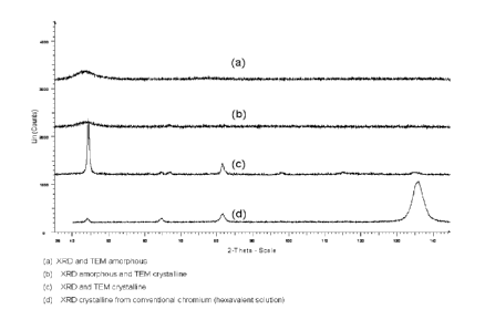
Fig. 1 includes four X-ray diffraction patterns (Cu k alpha) of two
embodiments of
nanogranular crystalline chromium alloy deposited in accordance with
embodiments of
the present invention, a hexavalent chromium of the prior art and an amorphous
chromium deposit not in accordance with the present invention.
Fig. 2 is a typical X-ray diffraction pattern (Cu k alpha) showing the
progressive
effect of annealing an amorphous chromium deposit from a trivalent chromium
bath of
the prior art.
Fig. 3 is a series of electron photomicrographs showing the macrocracking
effect
of annealing an initially amorphous chromium deposit from a trivalent chromium
bath of
the prior art.
Fig. 4 is a graphical chart illustrating how the concentration of sulfur in
one
embodiment of a chromium deposit relates to the XRD crystallinity of the
chromium
deposit.
Fig. 5 is a graphical chart comparing the crystal lattice parameter, in
Angstroms
(A) for (1) a crystalline chromium deposit in accordance with an embodiment of
the
7
CA 02700147 2010-03-18
WO 2009/046181
PCT/US2008/078561
present invention, compared with (2) crystalline chromium deposits from
hexavalent
chromium baths and (3) annealed amorphous-as-deposited chromium deposits.
Fig. 6 is a series of nine X-ray diffraction scans of electrodeposited
chromium
obtained by the methods disclosed by Sakamoto.
Fig. 7 is a graph illustrating the lattice parameter values obtained by the
present
inventors applying the deposition methods disclosed by Sakamoto and the
subsequently described lattice parameter determination method based upon the
modified Bragg equation.
Fig. 8 is a graph illustrating the 75 C Sargent Cr 6 data lattice parameter
values
obtained by the present inventors applying the deposition methods disclosed by
Sakamoto and evaluated using the subsequently described cos2/sin method.
Fig. 9 is a graphical presentation of various lattice parameters for chromium
obtained both from the literature and by carrying out the method of Sakamoto,
illustrating the consistency of the Sakamoto method lattice parameter data
obtained by
the present inventors with the known lattice parameters.
Fig. 10 is a high resolution transmission electron microscopy (TEM)
photomicrograph of a focused ion beam cross sectioned lamella from a
functional
crystalline chromium deposit in accordance with the present invention.
Figs. 11-13 are dark field TEM photomicrographs of a cross sectioned lamella
from chromium deposits in accordance with the present invention and
conventional
chromium deposit from a hexavalent chromium bath.
Figs. 14-17 are TEM diffraction pattern photomicrographs of chromium deposits,
in which the deposits are XRD crystalline, TEM crystalline but XRD amorphous,
both
XRD and TEM amorphous, and a conventional chromium deposit from a hexavalent
chromium bath and process, respectively.
Fig. 18 is a graph comparing Taber wear data for various chromium deposits,
including both conventional chromium deposits and a chromium deposit in
accordance
with the present invention.
It should be appreciated that the process steps and structures described below
may not necessarily form a complete process flow for manufacturing parts
containing
the functional crystalline chromium deposit of the present invention. The
present
invention can be practiced in conjunction with fabrication techniques
currently used in
8
CA 02700147 2010-03-18
WO 2009/046181
PCT/US2008/078561
the art, and only so much of the commonly practiced process steps are included
as are
necessary for an understanding of the present invention.
DETAILED DESCRIPTION
As used herein, a decorative chromium deposit is a chromium deposit with a
thickness less than one micron, and often less than 0.8 micron which is
primarily
decorative in purpose and use and is typically applied over an
electrodeposited nickel
or nickel alloy coating, or over a series of copper and nickel or nickel alloy
coatings
whose combined thicknesses are in excess of three microns, and which provide
the
protective or other functional characteristics of the coating.
As used herein, a functional chromium deposit is a chromium deposit applied to
(often directly to) a substrate such as strip steel EGGS (Electrolytically
Chromium
Coated Steel) where the chromium thickness is generally greater than 1 micron,
most
often greater than 3 microns, and is used for functional or industrial, not
decorative,
applications. Functional chromium deposits are generally applied directly to a
substrate
or over a relatively thin preparatory layer, in which the chromium layer, not
the
underlying layer(s), provides the sought protective or other functional
characteristics of
the coating. Functional chromium coatings take advantage of the special
properties of
chromium, including, e.g., its hardness, its resistance to heat, wear,
corrosion and
erosion, and its low coefficient of friction. Even though it has nothing to do
with
performance, many users want the functional chromium deposits to be like
decorative
chromium in appearance, so in some embodiments the functional chromium has a
decorative appearance in addition to its functional properties. The thickness
of the
functional chromium deposit may range from the above-noted greater than 1
micron or,
more often, to deposits having a thickness of 3 microns or much more, up to,
e.g., 1000
microns. In some cases, the functional chromium deposit is applied over a
'strike plate'
such as nickel or iron plating on the substrate or a 'duplex' system in which
the nickel,
iron or alloy coating has a thickness not usually greater than three microns
and the
chromium thickness generally is in excess of three microns.
The differences between decorative and functional chromium are well known to
those of skill in the art. Strict specifications for functional chromium
deposits have been
developed by such standard setting organizations as ASTM. See, e.g., ASTM B
650 ¨
95 (Reapproved 2002) relating to the specification for functional or hard
chromium,
which is also sometimes referred to as engineering chromium. As stated in ASTM
B
650, electrodeposited engineering chromium, which is also called "functional"
or "hard"
9
CA 02700147 2010-03-18
WO 2009/046181
PCT/US2008/078561
chromium, is usually applied directly to the basis metal and is much thicker
than
decorative chromium. As further stated in ASTM B 650, engineering chromium is
used
in the following exemplary purposes: to increase wear and abrasion resistance,
to
increase fretting resistance, to reduce static and kinetic friction, to reduce
galling or
seizing, or both, for various metal combinations, to increase corrosion
resistance and to
build up undersize or worn parts.
Decorative chromium plating baths are concerned with thin chromium deposits
over a wide plating range so that articles of irregular shape are completely
covered.
Functional chromium plating, on the other hand, is designed for thicker
deposits on
regularly shaped articles, where plating at a higher current efficiency and at
higher
current densities is important. Previous chromium plating processes employing
trivalent chromium ion have generally been suitable for forming only
"decorative"
finishes. The present invention provides "hard" or functional chromium
deposits, but is
not so limited, and can be used for decorative chromium finishes. "Hard",
"engineering"
or "functional" chromium deposits and "decorative" chromium deposits are known
terms
of art, as described above.
As used herein, when used with reference to, e.g., an electroplating bath or
other
composition, "substantially free of hexavalent chromium" means that the
electroplating
bath or other composition so described is free of any intentionally added
hexavalent
chromium. As will be understood, such a bath or other composition may contain
trace
amounts of hexavalent chromium present as an impurity in materials added to
the bath
or composition or as a by-product of electrolytic or chemical processes
carried out with
bath or composition. However, in accordance with the present invention,
hexavalent
chromium is not purposely or intentionally added to the baths or processes
disclosed
herein.
As used herein, macrocracks (and cognate terms such as macrocracking) are
defined as and refer to cracks (or formation of cracks) that extend through
the entire
thickness of the chromium layer, down to the substrate, and that are formed
primarily after
annealing at temperatures in the range from about 190 C to about 450 C for a
time
sufficient to crystallize an amorphous chromium deposit. Such time is
generally from about
1 to about 12 hours. Macrocracks primarily occur in chromium deposits that are
about 12
microns or greater in thickness, but can also occur in less thick chromium
deposits. As is
known in the art, macrocracks are generally only observed after the part
bearing the
chromium deposit of interest has been heated to temperatures in the above
range during
CA 02700147 2015-05-20
which the crystalline structure is formed from the amorphous material. The
minimum heat
treatment for embrittlement relief (i.e., annealing) of electrodeposited
chromium deposits is
spelled out in AMS-QQ-C-320 paragraph 3.2.6 as 375 F (190.5 C) for 3, 8, and
12 hours,
with the times dependent upon the desired tensile strength and/or Rockwell
hardness.
AMS-QQ-C-320 is the Aerospace Material Specification for Chromium Plating
(Electrodeposited) published by SAE International, Warrendale, PA. Under these
conditions, macrocracking can occur.
As used herein, the term "preferred orientation" carries the meaning that
would
be understood by those of skill in the crystallographic arts. Thus, "preferred
orientation"
is a condition of polycrystalline aggregate in which the crystal orientations
are not
random, but rather exhibit a tendency for alignment with a specific direction
in the bulk
material. Thus, a preferred orientation may be, for example, {100}, {110},
{111} and
integral multiples thereof, such as (222), in which the integral multiples of
a specifically
identified orientation, such as {111}, are deemed to be included with the
specifically
identified orientation, as would be understood by those of skill in the art.
Thus, as used
herein, reference to the {111} orientation includes integral multiples
thereof, such as
(222), unless otherwise specifically stated.
As used herein, the term "grain size" refers to the cross-sectional area of
grains
of the crystalline chromium deposit based on a TEM dark field image of
representative
or average grains, as determined using ImageJ 1.40 software, from the National
Institutes of Health. Using the "analyze particles" subroutine of ImageJ, edge
recognition of crystalline chromium grains may be obtained, the perimeters
traced, and
the areas calculated. ImageJ is well known for use in calculating the cross-
sectional
area of irregularly shaped particles by image analysis. Grain size is related
to the yield
strength of a material by relationships such as the Hall-Petch effect that
states that yield
strength increases as grain size decreases. Furthermore, it has been observed
that
small grains may improve corrosion resistance (see, e.g. U.S. Patent No.
6,174,610 for
its teachings relating to grain size).
As used herein, the term "nanogranular" refers to crystalline chromium grains
having an average grain size or cross-sectional area from about 100 square
nanometers (nm2) to about 5000 nm2, as determined by the above grain size
definition.
By comparison, a crystalline chromium deposit that is XRD crystalline
deposited
11
CA 02700147 2010-03-18
WO 2009/046181
PCT/US2008/078561
according to applicant's prior published application WO 2007/115030, the
crystalline
chromium grains have an average grain size or cross-sectional area in the
range from
about 9,000 nm2 to about 100,000 nm2, and conventional chromium deposits from
hexavalent chromium baths and processes have an average grain size or cross-
sectional area in the range from about 200,000 nm2 to about 800,000 nm2, and
larger.
Thus, there are clear differences between the nanogranular crystalline
chromium
deposits made in accordance with the present invention and those of other
methods.
As used herein, the term "TEM crystalline" means that a deposit so described
is
crystalline as determined by transmission electron microscopy (TEM). TEM is
capable
of determining that a deposit is crystalline when the crystal grains in the
deposit have a
size from about 1 nm and up, depending on the applied energy. A given material
may
be determined by TEM to be crystalline, when the same material is not
determined to
be crystalline by the usual X-ray diffraction technique in which X-rays from a
Cu ka
source are employed.
As used herein, the term "TEM amorphous" means that a deposit so described is
amorphous as determined by TEM. A deposit is TEM amorphous when it is not
found
to be TEM crystalline at applied energy of up to 200,000 eV. Using TEM, a
deposit is
confirmed to be amorphous when the selected area diffraction (SAD) pattern,
obtained
from TEM, has broad rings that lack "diffraction spots".
As used herein, the term "XRD crystalline" means that a deposit so described
is
crystalline as determined by X-ray diffraction (XRD) with a copper k alpha (Cu
ka) x-ray
source. Cu ka XRD has been commonly used to determine whether deposits are
crystalline for many years, and has long been the standard method of
determining
whether a given electrodeposited metal is or is not crystalline. In the prior
art,
essentially all determinations of crystallinity of chromium deposits have been
determined on one or both of two bases: (1) whether the chromium deposit forms
macrocracks when it is annealed at a temperature above about 190 C; and/or (2)
whether the deposit is or is not XRD crystalline as defined herein.
As used herein, the term "XRD amorphous" means that a deposit so described is
amorphous as determined by X-ray diffraction (XRD) with a copper k alpha (Cu
ka) X-
ray source.
As will be understood by those of skill in the art, sufficiently energetic X-
rays
from an appropriately high-energy X-ray source may be able to discern and/or
12
CA 02700147 2010-03-18
WO 2009/046181
PCT/US2008/078561
determine a grain size as small as 1 nm. Thus, the terms XRD crystalline and
XRD
amorphous, as used herein, are based on the use of a copper k alpha X-ray
source.
With respect to TEM and XRD crystalline materials, the present inventors have
discovered that some materials, such as certain embodiments of the chromium
deposits in accordance with the present invention, are not XRD crystalline,
but
nevertheless are TEM crystalline. A deposit that is XRD crystalline is always
TEM
crystalline, but a TEM crystalline deposit may or may not be XRD crystalline.
More
significantly, the present inventors have discovered that chromium deposits
having
superior properties, in terms of one or more of hardness, wear resistance,
durability and
brightness, can be obtained from trivalent chromium electroplating baths, when
the
deposits are TEM crystalline but are XRD amorphous. Thus, in one embodiment,
the
present invention relates to a crystalline functional chromium deposit that is
TEM
crystalline and is XRD amorphous, the deposit also having a grain size as
determined
by cross-sectional area of less than about 500 nm2 and in which the deposit
contains
carbon, nitrogen, oxygen and sulfur.
As used herein, the term "chromium (or Cr or chrome) deposit" includes both
chromium and chromium alloys in which the chromium alloy retains the BCC
crystal
structure of chromium deposits. As disclosed herein, in one embodiment, the
present
invention includes a chromium deposit containing chromium, carbon, oxygen,
nitrogen
and sulfur, and possibly also hydrogen.
Figs. 14-17 are TEM diffraction pattern photomicrographs of chromium deposits,
in which the deposits are XRD crystalline, TEM crystalline but XRD amorphous,
both
XRD and TEM amorphous, and a conventional chromium deposit from a hexavalent
chromium bath and process, respectively. As can be observed upon comparison of
the
photomicrographs in Figs. 14-17, the differences between the TEM diffraction
patterns
for these chromium deposits is quite apparent. In Fig. 14, the chromium
deposit is both
XRD crystalline and TEM crystalline, in accordance with one embodiment of the
present invention. Since the crystal grains in an XRD crystalline chromium
deposit are
relatively larger than the crystal grains in a deposit that is XRD amorphous
and TEM
crystalline, the diffraction pattern is stronger, presenting more discrete
exposure of the
film. In Fig. 15, the chromium deposit is XRD amorphous and TEM crystalline,
in
accordance with another embodiment of the present invention. Since the crystal
grains
are relatively smaller in a chromium deposit that is XRD amorphous and TEM
13
CA 02700147 2010-03-18
WO 2009/046181
PCT/US2008/078561
crystalline than one that is both XRD and TEM crystalline, the diffraction
pattern
includes smaller, discrete exposure points and rings of diffuse reflections.
In Fig. 16,
the deposit is both XRD amorphous and TEM amorphous, and is not in accordance
with the present invention. Since there are no crystal grains in a TEM
amorphous
chromium deposit, there are no discrete exposure points and relatively weak
rings of
diffuse reflections from the random chromium atoms in the deposit. Finally, in
Fig. 17,
for comparative purposes, a TEM diffraction pattern from a conventional
chromium
deposit from a hexavalent chromium bath and process is shown. Since the
crystal
grains in the conventional hexavalent chromium deposit are very much larger
than the
crystal grains in either alloy deposit according to the invention, i.e., a
deposit that is
both XRD and TEM crystalline or in a deposit that is XRD amorphous and TEM
crystalline, the diffraction pattern is much stronger, presenting very strong
discrete
exposure of the film, in a different pattern.
FUNCTIONAL CRYSTALLINE CHROMIUM ALLOY DEPOSITS
The present invention provides a reliably consistent body centered cubic (BCC
or bcc) functional crystalline chromium alloy deposit from a trivalent
chromium bath,
which bath is substantially free of hexavalent chromium, and in which the
deposit is
TEM crystalline as deposited, without requiring further treatment to
crystallize the
deposit, and in which the deposit is a functional chromium alloy deposit. In
one
embodiment, the invention provides a fiber texture nanogranular bcc
crystalline
functional chromium alloy deposit. In one embodiment, the electrodeposited
crystalline
functional chromium alloy deposit includes chromium, carbon, nitrogen, oxygen
and sulfur,
and the deposit is nanogranular as deposited. In some embodiments, the
chromium
deposit is both TEM crystalline and XRD crystalline, as well as nanogranular,
while in
other embodiments, the chromium deposit is TEM crystalline and XRD amorphous,
as
well as nanogranular. Thus, the present invention provides a solution to the
long-
standing, previously unsolved problem of obtaining a reliably consistent
crystalline
chromium deposit from an electroplating bath, and from a process, both of
which are
substantially free of hexavalent chromium.
In any of the embodiments of the present invention, the deposit may include
one
or any combination of two or more of:
a {111} preferred orientation;
an average crystal grain cross-sectional area of less than about 500 nm2; and
14
CA 02700147 2010-03-18
WO 2009/046181
PCT/US2008/078561
a lattice parameter of 2.8895 +/- 0.0025 A. In one embodiment, the deposit
includes a {111} preferred orientation and an average crystal grain cross-
sectional area
of less than about 500 nm2. In one embodiment, the deposit includes a {111}
preferred
orientation and a lattice parameter of 2.8895 +/- 0.0025 A. In one embodiment,
the
deposit includes an average crystal grain cross-sectional area of less than
about 500
nm2 and a lattice parameter of 2.8895 +/- 0.0025 A. In one embodiment, the
deposit
includes a {111} preferred orientation, an average crystal grain cross-
sectional area of
less than about 500 nm2, and a lattice parameter of 2.8895 +/- 0.0025 A.
In any of the embodiments of the invention described herein, the deposit may
include from about 0.05 wt.% to about 20 wt.% sulfur. The deposit may include
nitrogen, in an amount from about 0.1 to about 5 wt% nitrogen. The deposit may
include carbon, in an amount of carbon less than that amount which renders the
chromium deposit amorphous. In one embodiment, the deposit may include from
about
0.07 wt.% to about 1.4 wt.% sulfur, from about 0.1 wt.% to about 3 wt.%
nitrogen, and
from about 0.1 wt.% to about 10 wt.% carbon. The deposit, in one embodiment,
further
comprises oxygen, from about 0.5 wt.% to about 7 wt.% of the deposit, and in
another
embodiment further comprises oxygen from about 1 wt.% to about 5 wt.%. The
deposit
may also contain hydrogen.
To accurately determine sulfur content at low concentrations PIXE is employed.
PIXE is an x-ray fluorescence method which can detect elements with atomic
numbers
greater than lithium but can not accurately quantify elements with low atomic
numbers
including carbon, nitrogen, and oxygen. Therefore, with PIXE, only chromium
and
sulfur can be accurately reported in a quantitative manner and the values are
for these
two elements only (e.g., the relative quantities do not account for other
alloying
elements). XPS can quantify low z elements except for hydrogen, but it does
not have
the sensitivity of PIXE, and it samples only a very thin sample volume.
Therefore, the
alloy content is determined using XPS after sputtering away surface oxides and
penetrating into the bulk region of the coating using an argon ion beam. The
XPS
spectra is then obtained and while it does not include the likely presence of
hydrogen,
which can not be detected by XPS, the spectrum does effectively determine the
relative
amounts of carbon, nitrogen, oxygen, and chromium present in the material.
From the
values obtained by XPS and PIXE, the total content of chromium, carbon,
nitrogen
oxygen and sulfur in the alloy can be calculated by those of ordinary skill in
the art. In
CA 02700147 2010-03-18
WO 2009/046181
PCT/US2008/078561
the present disclosure, all sulfur contents reported for the deposits are as
determined
by PIXE. In the present disclosure, all carbon, nitrogen and oxygen contents
reported
for the deposits are as determined by XPS. Chromium content reported for the
deposits is determined by both methods.
In one embodiment, the crystalline chromium deposit of the present invention
is
substantially free of macrocracks, using standard test methods. That is, in
this
embodiment, under standard test methods, substantially no macrocracks are
observed
when samples of the chromium deposited are examined.
In one embodiment, the crystalline chromium deposit is substantially free of
formation of macrocracks after exposure to elevated temperatures for extended
periods. In one embodiment, the crystalline chromium deposit does not form
macrocracks when heated to a temperature up to about 190 C for a period of
about 1 to
about 10 hours. In one embodiment, the crystalline chromium deposit does not
change
its crystalline structure when heated to a temperature up to about 190 C. In
one
embodiment, the crystalline chromium deposit does not form macrocracks when
heated
to a temperature up to about 250 C for a period of about 1 to about 10 hours.
In one
embodiment, the crystalline chromium deposit does not change its crystalline
structure
when heated to a temperature up to about 250 C. In one embodiment, the
crystalline
chromium deposit does not form macrocracks when heated to a temperature up to
about 300 C for a period of about 1 to about 10 hours. In one embodiment, the
crystalline chromium deposit does not change its crystalline structure when
heated to a
temperature up to about 300 C..
Thus, in one embodiment, the crystalline chromium deposit wherein the deposit
remains substantially free of macrocracking when subjected to a temperature of
at least
190 C for at least 3 hours. In another embodiment, the deposit remains
substantially
free of macrocracking when subjected to a temperature of at least 190 C for at
least 8
hours. In yet another embodiment, the deposit remains substantially free of
macrocracking when subjected to a temperature of at least 190 C for at least
12 hours.
In one embodiment, the crystalline chromium deposit wherein the deposit
remains
substantially free of macrocracking when subjected to a temperature up to 350
C for at
least 3 hours. In another embodiment, the deposit remains substantially free
of
macrocracking when subjected to a temperature up to 350 C for at least 8
hours. In
16
CA 02700147 2010-03-18
WO 2009/046181
PCT/US2008/078561
yet another embodiment, the deposit remains substantially free of
macrocracking when
subjected to a temperature up to 350 C for at least 12 hours.
In one embodiment, the nanogranular functional crystalline chromium alloy
deposit in accordance with the present invention has a cubic lattice parameter
of
2.8895 +/- 0.0025 Angstroms (A). It is noted that the term "lattice parameter"
is also
sometimes used as "lattice constant". For purposes of the present invention,
these
terms are considered synonymous. It is noted that for body centered cubic
crystalline
chromium, there is a single lattice parameter, since the unit cell is cubic.
This lattice
parameter is more properly referred to as a cubic lattice parameter, since the
crystal
lattice of the crystalline chromium deposit of the present invention is a body
centered
cubic crystal, but herein is referred to simply as the "lattice parameter",
with the
understanding that, for the bcc chromium of the present invention, this refers
to the
cubic lattice parameter. In one embodiment, the crystalline chromium deposit
in
accordance with the present invention has a lattice parameter of 2.8895 A +/-
0.0020 A.
In another embodiment, the crystalline chromium deposit in accordance with the
present invention has a lattice parameter of 2.8895 A +/- 0.0015 A. In yet
another
embodiment, the crystalline chromium deposit in accordance with the present
invention
has a lattice parameter of 2.8895 A +/- 0.0010 A. Some specific examples are
provided
herein of crystalline chromium deposits having lattice parameters within these
ranges.
The lattice parameters reported herein for the nanogranular functional
crystalline
chromium alloy deposit of the present invention are measured for the chromium
deposit
as deposited but these lattice parameters generally do not substantially
change with
annealing. The present inventors have measured the lattice parameter on
samples of
crystalline chromium deposits in accordance with the present invention (1) as
deposited, (2) after annealing at 350 C for one hour and cooling to room
temperature,
(3) after a second annealing at 450 C and cooling to room temperature, and (4)
after a
third annealing at 550 C and cooling to room temperature. No change in lattice
parameter is observed in (1)-(4). The present inventors generally carry out X-
ray
diffraction ("XRD") experiments in-situ in a furnace built into an XRD
apparatus
manufactured by Anton Parr. The present inventors generally perform not do the
grinding and cleaning process described below. Thus, in one embodiment of the
present invention, the lattice parameter of the nanogranular functional
crystalline
chromium alloy deposit does not vary upon annealing at temperatures up to 550
C. In
17
CA 02700147 2010-03-18
WO 2009/046181
PCT/US2008/078561
another embodiment, the lattice parameter of the functional crystalline
chromium
deposit does not vary upon annealing at temperatures up to 450 C. In another
embodiment, the lattice parameter of the functional crystalline chromium
deposit does
not vary upon annealing at temperatures up to 350 C.
Elemental crystalline chromium has a lattice parameter of 2.8839 A which has
been determined by numerous experts and reported by standards organizations
such
as the National Institute of Standards and Technology. A typical determination
uses
electrodeposited chromium from high purity chromic acid salts as reference
material
(ICD PDF 6-694, from Swanson, et al., Natl. Bur. Stand. (U.S.) Orc. 539, V, 20
(1955) ).
This material is then crushed, acid washed, annealed in hydrogen and then
helium at
1200 C to allow grain growth and diminish internal stress, carefully cooled at
100 C per
hour to room temperature in helium, then measured.
In all the literature on chromium lattice parameters there is a single
reference to
lattice parameter exceeding 2.887A. This reference is by Sakamoto who reported
preparation of chromium electrodeposits on brass substrates from solutions
that had
different plating temperatures from 30 C to 75 C and measured lattice
parameters of
the as-deposited chromium on brass without consideration for residual stress.
Attempts
to duplicate Sakamoto's results ignoring residual stress have been fruitless.
As
discussed in more detail below, when the present inventors measured the
lattice
parameter as a function of temperature, using two different instruments, the
results
agreed with each other, and the lattice parameter values ranged from 2.8812 to
2.883 A,
with a mean of 2.8821 A and a standard deviation of 0.0006 A, and did not show
an
increase in lattice parameter as bath temperature was increased. Further
discussion of
the present inventors' attempts to duplicate the Sakamoto results are provided
hereinbelow.
Crystalline chromium electrodeposited from a hexavalent chromium bath has a
lattice parameter ranging from about 2.8809 A to about 2.8858 A.
Annealed electrodeposited trivalent amorphous-as-deposited chromium has a
lattice parameter ranging from about 2.8818 A to about 2.8852 A, but also has
macrocracks.
Thus, the lattice parameter of the nanogranular functional crystalline
chromium
alloy deposit in accordance with the present invention is larger than the
lattice
parameter of other known forms of crystalline chromium. Although not to be
bound by
18
CA 02700147 2010-03-18
WO 2009/046181
PCT/US2008/078561
theory, it is considered that this difference may be due to the incorporation
of the
heteroatoms in the alloy, e.g., sulfur, nitrogen, carbon, oxygen and possibly
hydrogen,
into the crystal lattice of the deposit obtained in accordance with the
present invention.
In one embodiment, the nanogranular functional crystalline chromium alloy
deposit in accordance with the invention has a {111} preferred orientation. As
noted,
the deposit may have, e.g., a (222) preferred orientation, which is understood
to be
within the {111} preferred orientation description and "family".
In one embodiment, the crystalline chromium deposit contains from about 0.05
wt.% to about 20 wt.% sulfur. In another embodiment, the chromium deposit
contains
from about 0.07 wt.% to about 1.4 wt.% sulfur. In another embodiment, the
chromium
deposit contains from about 1.5 wt.% to about 10 wt.% sulfur. In another
embodiment,
the chromium deposit contains from about 1.7 wt.% to about 4 wt.% sulfur. The
sulfur
is in the deposit present as elemental sulfur and may be a part of crystal
lattice, i.e.,
replacing and thus taking the position of a chromium atom in the crystal
lattice or taking
a place in the tetrahedral or octahedral hole positions and distorting the
lattice. In one
embodiment, the source of sulfur may be a divalent sulfur compound. More
details on
exemplary sulfur sources are provided below.
In one embodiment, the nanogranular functional crystalline chromium alloy
deposit contains from about 0.1 to about 5 wt% nitrogen. In another
embodiment, the
deposit contains from about 0.5 to about 3 wt% nitrogen. In another embodiment
the
deposit contains about 0.4 weight percent nitrogen.
In one embodiment, the nanogranular functional crystalline chromium alloy
deposit contains from about 0.1 to about 5 wt% carbon. In another embodiment,
the
deposit contains from about 0.5 to about 3 wt% carbon. In another embodiment
the
deposit contains about 1.4 wt.% carbon. In one embodiment, the crystalline
contains
an amount of carbon less than that amount which renders the deposit amorphous.
That
is, above a certain level, e.g., in one embodiment, above about 10 wt.`)/0,
the carbon
renders the deposit amorphous, and therefore takes it out of the scope of the
present
invention. Thus, the carbon content should be controlled so that it does not
render the
deposit amorphous. The carbon may be present in the deposit as elemental
carbon or
as carbide carbon. If the carbon is present in the deposit as elemental
carbon, it may
be present either as graphitic or as amorphous carbon.
In one embodiment, the nanogranular functional crystalline chromium alloy
deposit contains from about 0.1 to about 5 wt% oxygen. In another embodiment,
the
19
CA 02700147 2010-03-18
WO 2009/046181
PCT/US2008/078561
deposit contains from about 0.5 to about 3 wt% nitrogen. In another embodiment
the
deposit contains about 0.4 weight percent nitrogen.
In one embodiment, the TEM crystalline, XRD amorphous nanogranular
functional chromium alloy deposit contains from about 0.06 wt.% to about 1.5
wt.%
sulfur, and in one embodiment, the TEM crystalline, XRD amorphous deposit
contains
from about 0.06 wt.% to less than 1 wt.% sulfur (e.g., up to about 0.95 or up
to about
0.90 wt.% sulfur). The TEM crystalline, XRD amorphous deposit generally
contains
from about 0.1 wt.% to about 5 wt.% nitrogen, and from about 0.1 wt.% to about
10
wt.% carbon. In one embodiment, the TEM crystalline, XRD amorphous deposit
contains from about 0.05 wt.% to less than 4 wt.% sulfur (e.g., up to about
3.9 wt.%
sulfur), from about 0.1 wt.% to about 5 wt.% nitrogen, and from about 0.1 wt.%
to about
10 wt.`)/0 carbon.
In one embodiment, the XRD crystalline chromium alloy deposit contains from
about 4 wt.% to about 20 wt.% sulfur, from about 0.1 wt.% to about 5 wt.%
nitrogen,
and from about 0.1 wt.% to about 10 wt.% carbon.
In one embodiment, the TEM crystalline, XRD amorphous deposit of the present
invention has grain size, as measured by cross-sectional area as described
above,
orders of magnitude smaller than that observed with deposits from hexavalent
chromium, and has grain size substantially smaller than can be obtained with
higher
sulfur contents. Hexavalent chromium deposits have an average grain size or
cross-
sectional area in the range from about 200,000 nm2 to about 800,000 nm2, and
larger,
as determined by the ImageJ software.
In one embodiment, the nanogranular functional crystalline chromium alloy
deposit of the present invention, on average, have an average grain size or
cross-
sectional area in the range from about 100 square nanometers (nm2) to about
5000
nm2, as determined by the ImageJ software. In one embodiment, the nanogranular
functional crystalline chromium alloy deposit of the present invention, on
average, have
an average grain size or cross-sectional area in the range from about 300
square
nanometers (nm2) to about 4000 nm2, as determined by the ImageJ software. In
one
embodiment, the nanogranular functional crystalline chromium alloy deposit of
the
present invention, on average, have an average grain size or cross-sectional
area in
the range from about 600 square nanometers (nm2) to about 2500 nm2, as
determined
by the ImageJ software. It is noted that these are average sizes, and to
determine the
CA 02700147 2010-03-18
WO 2009/046181
PCT/US2008/078561
average, a suitable number of grains should be examined, as readily determined
by the
person of skill in the art.
In one embodiment, the grains of the nanogranular functional crystalline
chromium alloy deposit of the present invention, on average, have a width less
than 50
nm and do not have axes elongated more than about five times (5X) the grain
size,
although many small grains with similar orientation may be stacked above each
other.
In other embodiments, the grain size is significantly less than 50 nm, as
discussed
below in more detail. This stacking may be due to the fiber having been
disrupted and
made discontinuous, like a strand of pearls, rather than continuous as is the
case with
chromium from hexavalent solution.
In one embodiment, the nanogranular functional crystalline chromium alloy
deposit of the present invention includes an average chromium alloy crystal
grain width
less than 70 nanometers (nm). In another embodiment, the deposit includes an
average chromium crystal grain width less than about 50 nm. In another
embodiment,
the deposit includes an average chromium crystal grain width less than about
30 nm.
In one embodiment, the deposit includes an average chromium crystal grain
width in
the range from about 20 nm to about 70 nm, and in another embodiment, in the
range
from about 30 to about 60 nm. In one embodiment, the grain width of the
deposits of
the present invention are less than 20 nm, and in one embodiment, the grain
width of
the deposit has an average grain width in the range from 5 nm to 20 nm.
Smaller grain size is correlated to increasing hardness of the chromium
deposit
in accordance with the Hall-Petch effect, down to some minimum grain size in
accordance with the reverse Hall-Petch effect. While smaller grain size is
known to be
related to greater strength, the small grain size attainable with the present
invention, in
combination with the other features of the present invention, provides a
further novel
aspect to the present invention.
In one embodiment of the present invention, the nanogranular functional
crystalline chromium alloy deposit exhibits a microhardness in the range from
about 50
to about 150 Vickers greater than the Vickers hardnesses obtained for
hexavalent-
derived chromium deposits, and in one embodiment, from about 100 to about 150
Vickers greater than comparable hexavalent-derived deposits (hardness
measurements
taken with a 25 gram load). Thus, in one embodiment, the functional
crystalline
chromium deposits in accordance with the present invention exhibit Vickers
hardness
values, measured under a 25 gram load, in the range from about 950 to about
1100,
21
CA 02700147 2010-03-18
WO 2009/046181
PCT/US2008/078561
and in another embodiment from about 1000 to about 1050. Such hardness values
are
consistent with the small grain size noted above and are greater than the
hardness
values observed with functional chromium deposits obtained from hexavalent
chromium
electrodeposition baths.
PROCESSES FOR DEPOSITION OF FUNCTIONAL CRYSTALLINE CHROMIUM
ALLOY FROM TRIVALENT CHROMIUM BATHS
During the process of electrodepositing the nanogranular functional
crystalline
chromium alloy deposit of the present invention, the electrical current is
applied at a
current density of at least about 10 amperes per square decimeter (A/dm2). In
another
embodiment, the current density is in the range from about 10 A/dm2 to about
200
A/dm2, and in another embodiment, the current density is in the range from
about 10
A/dm2 to about 100 A/dm2, and in another embodiment, the current density is in
the
range from about 20 A/dm2 to about 70 A/dm2, and in another embodiment, the
current
density is in the range from about 30 A/dm2 to about 60 A/dm2, during the
electrodeposition of the deposit from the trivalent chromium bath in
accordance with the
present invention.
During the process of electrodepositing the nanogranular functional
crystalline
chromium alloy deposit of the present invention, the electrical current may be
applied to
the bath using any one or any combination of two or more of direct current,
pulse
waveform or pulse periodic reverse waveform.
In one embodiment, the present invention provides a process for
electrodepositing a nanogranular functional crystalline chromium alloy deposit
on a
substrate, including providing an electrodeposition bath, in which the bath is
prepared
by combining ingredients comprising trivalent chromium, a source of divalent
sulfur, a
carboxylic acid, a source of sp3 nitrogen, and in which the bath is
substantially free of
hexavalent chromium; immersing a substrate in the electroplating bath; and
applying an
electrical current to electrodeposit a functional crystalline chromium deposit
on the
substrate, in which the alloy includes chromium, carbon, nitrogen, oxygen and
sulfur,
and the deposit is crystalline and nanogranular as deposited. In one
embodiment, the
deposit is both TEM and XRD crystalline. In one embodiment, the deposit is TEM
crystalline and is XRD amorphous. In one embodiment, the deposit further
includes
one or any combination of two or more of (a) a {111} preferred orientation;
(b) an
22
CA 02700147 2010-03-18
WO 2009/046181
PCT/US2008/078561
average crystal grain cross-sectional area of less than about 500 nm2; and (c)
a lattice
parameter of 2.8895 +/- 0.0025 A.
The contents of the components of the chromium alloy deposit, and the various
physical features and properties of the deposit obtained by the process are
described
above, with respect to the deposit, and are not repeated here for brevity.
In one embodiment, the source of sp3 nitrogen includes ammonium hydroxide or
a salt thereof, a primary, secondary or tertiary alkyl amine, in which the
alkyl group is a
01-06 alkyl, an amino acid, a hydroxy amine, or a polyhydric alkanolamines,
wherein
alkyl groups in the source of nitrogen comprise 01-06 alkyl groups. In one
embodiment,
the source of sp3 nitrogen may be ammonium chloride and in another embodiment,
ammonium bromide, and in another embodiment, a combination of both ammonium
chloride and ammonium bromide.
In one embodiment, the carboxylic acid includes one or more of formic acid,
oxalic acid, glycine, acetic acid, and malonic acid or a salt of any thereof.
The
carboxylic acid provides both carbon and oxygen, which may be incorporated
into the
chromium alloy deposit of the present invention. Other carboxylic acids may be
used,
as will be recognized.
In one embodiment, the source of divalent sulfur comprises one or a mixture of
two or more of:
thiomorpholine,
thiodiethanol,
L-cysteine,
L-cystine,
allyl sulfide,
thiosalicylic acid,
thiodipropanoic acid,
3,3'-dithiodipropanoic acid,
3-(3-aminopropyl disulfanyl) propylamine hydrochloride,
[1,3]thiazin-3-ium chloride,
thiazolidin-3-ium dichloride,
a compound referred to as a 3-(3-aminoalkyl disulfenyl) alkylamine having the
formula:
23
CA 02700147 2010-03-18
WO 2009/046181
PCT/US2008/078561
R341)-(CH2)n-S-S-(CH2)r,NR13 2 xe
wherein R and R1 are independently H, methyl or ethyl and n and m are
independently
1-4; or
a compound referred to as a [1,3] thiazin-3-ium having the formula:
zN /R
S N
\ _______________________________________ I\R1
in which R and R1 are independently H, methyl or ethyl; or
a compound referred to as a thiazolidin-3-ium having the formula:
S
e))
Xe
N
/\
R R1
in which R and R1 are independently H, methyl or ethyl; and
in which in each of the foregoing sources of divalent sulfur, X may be any
halide
or an anion other than nitrate (-NO3-), comprising one or more of cyano,
formate,
citrate, oxalate, acetate, malonate, SO4-2, PO4-3, H2P03-1, H2P02-1,
Pyrophosphate
(P2074), Polyphosphate (P3010-5), partial anions of the foregoing multivalent
anions,
e.g., HSO4-1 , HPO4-2, H2PO4-1 , C1-C18 alkyl sulfonic acids, Ci-C18 benzene
sulfonic
acids, and sulfamate.
In one embodiment, the source of divalent sulfur is not saccharine.
In one embodiment, the source of divalent sulfur is not thiourea.
In one embodiment, the source of divalent sulfur is present in the
electrodeposition bath at a concentration from about 0.0001 M to about 0.05 M.
In one
embodiment, the source of divalent sulfur is present in the bath at a
concentration
sufficient to obtain a deposit that is both XRD and TEM crystalline. In one
embodiment,
the concentration of divalent sulfur in the bath that is sufficient to obtain
such a deposit
that is both XRD and TEM crystalline is in the range from about 0.01 M to
about 0.10 M.
24
CA 02700147 2010-03-18
WO 2009/046181
PCT/US2008/078561
In another embodiment, the source of divalent sulfur is present in the bath at
a
concentration sufficient to obtain a deposit that is XRD amorphous and TEM
crystalline.
In one embodiment, the concentration of divalent sulfur in the bath that is
sufficient to
obtain such a deposit that is XRD amorphous and TEM crystalline is in the
range from
about 0.0001 M to less than about 0.01 M.
In one embodiment, the electrodeposition bath has a pH in the range from 5 to
about 6.5. In one embodiment, the electrodeposition bath has a pH in the range
from 5
to about 6. In one embodiment, the electrodeposition bath has a pH of about
5.5. At a
pH outside the disclosed range, e.g., at about pH 4 and less, and at about pH
7 or
greater, components of the bath begin to precipitate or the bath does not
function as
desired.
In one embodiment, the step of applying an electrical current is carried out
for a
time sufficient to form the deposit to a thickness of at least 3 microns. In
one
embodiment, the step of applying an electrical current is carried out for a
time sufficient
to form the deposit to a thickness of at least 10 microns. In one embodiment,
the step
of applying an electrical current is carried out for a time sufficient to form
the deposit to
a thickness of at least 15 microns.
In one embodiment, the cathodic efficiency ranges from about 5% to about 80%,
and in one embodiment, the cathodic efficiency ranges from about 10% to about
40%,
and in another embodiment, the cathodic efficiency ranges from about 20% to
about
30%.
These processes in accordance with the invention may be carried out under the
conditions described herein, and in accordance with standard practices for
electrodeposition of chromium. Thus, any conditions not specifically stated
herein may
be set as for any conventional chromium electroplating process, as long as it
does not
depart from the scope of the present disclosure.
TRIVALENT CHROMIUM ELECTRODEPOSITION BATHS
In one embodiment, the present invention relates to an electrodeposition bath
for
electrodepositing the above-described nanogranular crystalline functional
chromium
alloy deposit, in which the alloy comprises chromium, carbon, nitrogen, oxygen
and
sulfur, and the bath includes an aqueous solution obtained by combining
ingredients
including a source of trivalent chromium having a concentration of least 0.1
molar and
being substantially free of added hexavalent chromium; a carboxylic acid; a
source of
CA 02700147 2010-03-18
WO 2009/046181
PCT/US2008/078561
sp3 nitrogen; a source of divalent sulfur, at a concentration in the range
from about
0.0001 M to about 0.05 M; and in which the bath further includes a pH in the
range from
to about 6.5; an operating temperature in the range from about 35 C to about
95 C;
and a source of electrical energy to be applied between an anode and a cathode
5 immersed in the electrodeposition bath.
This bath is generally a trivalent chromium electroplating bath, and in
accordance with the present invention is substantially free of hexavalent
chromium. In
one embodiment, the bath is free of detectable amounts of hexavalent chromium.
In
the baths of the present invention, hexavalent chromium is not intentionally
or
purposefully added. It is possible that some hexavalent chromium will be
formed as a
by-product, or that there may be some small quantity of hexavalent chromium
impurity
present, but this is neither sought nor desired. Suitable measures may be
taken to
avoid such formation of hexavalent chromium, as known in the art.
The trivalent chromium may be supplied as chromic chloride, CrCI3, chromic
fluoride, CrF3, chromic oxide, Cr203, chromic phosphate, CrPO4, or in a
commercially
available solution such as chromium hydroxy dichloride solution, chromic
chloride
solution, or chromium sulfate solution, e.g., from McGean Chemical Company or
Sentury Reagents. Trivalent chromium is also available as chromium
sulfate/sodium or
potassium sulfate salts, e.g., Cr(OH)SO4.1\1a2SO4, often referred to as
chrometans or
kromtans, chemicals useful for tanning of leather, and available from
companies such
as Elementis, Lancashire Chemical, and Soda Sanayii. As noted below, the
trivalent
chromium may also be provided as chromic formate, Cr(HC00)3 from Sentury
Reagents. If provided as chromic formate, this would provide both the
trivalent
chromium and the carboxylic acid.
The concentration of the Cr 3 ions may be in the range from about 0.1 molar
(M)
to about 5 M. In one embodiment, the electrodeposition bath contains Cr 3 ions
at a
concentration in the range from about 0.1 M to about 2 M. The higher the
concentration
of trivalent chromium, the higher the current density that can be applied
without
resulting in a dendritic deposit, and consequently the faster the rate of
crystalline
chromium deposition that can be achieved.
In one embodiment, the electrodeposition bath contains a quantity of the
divalent
sulfur compound sufficient that the chromium deposit comprises from about 0.05
wt.%
to about 20 wt.% sulfur. In one embodiment, the concentration of the divalent
sulfur
26
CA 02700147 2010-03-18
WO 2009/046181
PCT/US2008/078561
compound in the bath may range from about 0.1 g/I to about 25 g/I, and in one
embodiment, the divalent sulfur compound in the bath may range from about 1
g/I to
about 5 g/I.
The trivalent chromium bath may further include a carboxylic acid such as
formic
acid or a salt thereof, such as one or more of sodium formate, potassium
formate,
ammonium formate, calcium formate, magnesium formate, etc. Other organic
additives, including amino acids, such as glycine, and thiocyanate may also be
used to
produce crystalline chromium deposits from trivalent chromium and their use is
within
the scope of one embodiment of this invention. As noted above, chromium (III)
formate, Cr(H000)3, may be used as a source of both trivalent chromium and
formate.
At the pH of the bath, the formate will be present in a form to provide formic
acid.
In one embodiment, the electrodeposition bath contains a quantity of the
carboxylic acid sufficient that the chromium deposit comprises an amount of
carbon
less than that amount which renders the chromium deposit amorphous. In one
embodiment, the concentration of the carboxylic acid in the bath may range
from about
0.1 M to about 4 M.
The trivalent chromium bath may further include a source of nitrogen, which
may
be in the form of ammonium hydroxide or a salt thereof, or may be a primary,
secondary or tertiary alkyl amine, in which the alkyl group is a C1-C6 alkyl.
In one
embodiment, the source of nitrogen is other than a quaternary ammonium
compound.
In addition, amino acids, hydroxy amines such as quadrol and polyhydric
alkanolamines, can be used as the source of nitrogen. In one embodiment of
such
nitrogen sources, the additives include Ci-C6 alkanol groups. In one
embodiment, the
source of nitrogen may be added as a salt, e.g., an amine salt such as a
hydrohalide
salt.
In one embodiment, the electrodeposition bath contains a quantity of the
source
of nitrogen sufficient that the chromium deposit comprises from about 0.1 to
about 5
wt% nitrogen. In one embodiment, the concentration of the source of nitrogen
in the
bath may range from about 0.1 M to about 6 M.
As noted above, the crystalline chromium deposit may include carbon. The
carbon source may be, for example, the organic compound such as formic acid or
formic acid salt included in the bath. Similarly, the crystalline chromium may
include
oxygen and hydrogen, which may be obtained from other components of the bath
27
CA 02700147 2010-03-18
WO 2009/046181
PCT/US2008/078561
including electrolysis of water, or may also be derived from the formic acid
or salt
thereof, or from other bath components.
In addition to the chromium atoms in the crystalline chromium deposit, other
metals may be co-deposited. As will be understood by those of skill in the
art, such
metals may be suitably added to the trivalent chromium electroplating bath as
desired
to obtain various crystalline alloys of chromium in the deposit. Such metals
include, but
are not necessarily limited to, Re, Cu, Fe, W, Ni, Mn, and may also include,
for
example, P (phosphorus). In fact, all elements electrodepositable from aqueous
solution, directly or by induction, as described by Pourbaix (Pourbaix, M.,
"Atlas of
Electrochemical Equilibria", 1974, NAGE (National Association of Corrosion
Engineers))
or by Brenner (Brenner, A., "Electrodeposition of Alloys, Vol. I and Vol. II",
1963,
Academic Press, NY) may be alloyed in this process. In one embodiment, the
alloyed
metal is other than aluminum. As is known in the art, metals
electrodepositable from
aqueous solution include: Ag, As, Au, Bi, Cd, Co, Cr, Cu, Ga, Ge, Fe, In, Mn,
Mo, Ni, P,
Pb, Pd, Pt, Rh, Re, Ru, S, Sb, Se, Sn, Te, TI, W and Zn, and inducible
elements include
B, C and N. As will be understood by those of skill in the art, the co-
deposited metal or
atom is present in an amount less than the amount of chromium in the deposit,
and the
deposit obtained thereby often should be body-centered cubic crystalline, as
is the
crystalline chromium deposit of the present invention obtained in the absence
of such
co-deposited metal or atom.
The trivalent chromium bath further comprises a pH of at least 5, and the pH
can
range up to at least about 6.5. In one embodiment, the pH of the trivalent
chromium
bath is in the range from about 5 to about 6.5, and in another embodiment the
pH of the
trivalent chromium bath is in the range from about 5 to about 6, and in
another
embodiment, the pH of the trivalent chromium bath is about 5.5, and in another
embodiment, the pH of the trivalent chromium bath is in the range from about
5.25 to
about 5.75.
In one embodiment, the trivalent chromium bath is maintained at a temperature
in the range from about 35 C to about 115 C or the boiling point of the
solution,
whichever is less, during the process of electrodepositing the crystalline
chromium
deposit of the present invention. In one embodiment, the bath temperature is
in the
range from about 45 C to about 75 C, and in another embodiment, the bath
temperature is in the range from about 50 C to about 65 C, and in one
embodiment,
28
CA 02700147 2010-03-18
WO 2009/046181
PCT/US2008/078561
the bath temperature is maintained at about 55 C, during the process of
electrodepositing the crystalline chromium deposit.
As noted above, a source of divalent sulfur is preferably provided in the
trivalent
chromium electroplating bath. A wide variety of divalent sulfur-containing
compounds
can be used in accordance with the present invention.
In one embodiment, the source of divalent sulfur may be any one of those
described above with respect to the bath disclosed in the process embodiment.
In another embodiment, the source of divalent sulfur may include one or a
mixture of two or more of a compound having the general formula (I):
)(1¨R1¨(s)n¨R2¨)(2 (1)
wherein in (I), X1 and X2 may be the same or different and each of X1 and X2
independently comprise hydrogen, halogen, amino, cyano, nitro, nitroso, azo,
alkylcarbonyl, formyl, alkoxycarbonyl, aminocarbonyl, alkylamino,
dialkylamino,
alkylaminocarbonyl, dialkylaminocarbonyl, carboxyl (as used herein, "carboxyl"
includes
all forms of carboxyl groups, e.g., carboxylic acids, carboxylic alkyl esters
and
carboxylic salts), sulfonate, sulfinate, phosphonate, phosphinate, sulfoxide,
carbamate,
polyethoxylated alkyl, polypropoxylated alkyl, hydroxyl, halogen-substituted
alkyl,
alkoxy, alkyl sulfate ester, alkylthio, alkylsulfinyl, alkylsulfonyl,
alkylphosphonate or
alkylphosphinate, wherein the alkyl and alkoxy groups are C1-C6, or X1 and X2
taken
together may form a bond from R1 to R2, thus forming a ring containing the R1
and R2
groups,
wherein R1 and R2 may be the same or different and each of R1 and R2
independently comprise a single bond, alkyl, allyl, alkenyl, alkynyl,
cyclohexyl, aromatic
and heteroaromatic rings, alkoxycarbonyl, aminocarbonyl, alkylaminocarbonyl,
dialkylaminocarbonyl, polyethoxylated and polypropoxylated alkyl, wherein the
alkyl
groups are Ci-C6, and
wherein n has an average value ranging from 1 to about 5.
In one embodiment, the source of divalent sulfur may include one or a mixture
of
two or more of a compound having the general formula (11a) and/or (11b):
29
CA 02700147 2010-03-18
WO 2009/046181
PCT/US2008/078561
rxR5
R44 Sk............
and/or R R5
X
R3 R6 R3 m
6
(11a) (11b)
wherein in (11a) and (11b), R3, R4, R5 and R6 may be the same or different and
independently comprise hydrogen, halogen, amino, cyano, nitro, nitroso, azo,
alkylcarbonyl, formyl, alkoxycarbonyl, aminocarbonyl, alkylamino,
dialkylamino,
alkylaminocarbonyl, dialkylaminocarbonyl, carboxyl, sulfonate, sulfinate,
phosphonate,
phosphinate, sulfoxide, carbamate, polyethoxylated alkyl, polypropoxylated
alkyl,
hydroxyl, halogen-substituted alkyl, alkoxy, alkyl sulfate ester, alkylthio,
alkylsulfinyl,
alkylsulfonyl, alkylphosphonate or alkylphosphinate, wherein the alkyl and
alkoxy
groups are 01-06,
wherein X represents carbon, nitrogen, oxygen, sulfur, selenium or tellurium
and
in which m ranges from 0 to about 3,
wherein n has an average value ranging from 1 to about 5, and
wherein each of (11a) or (11b) includes at least one divalent sulfur atom.
In one embodiment, the source of divalent sulfur may include one or a mixture
of
two or more of a compound having the general formula (111a) and/or (111b):
R ,1Sx42 R5 R4 S).4k R5
and/or I
X
R3 R6 R3 m
6
(111a) (111b)
wherein, in (111a) and (111b), R3, R4, R5 and R6 may be the same or different
and
independently comprise hydrogen, halogen, amino, cyano, nitro, nitroso, azo,
alkylcarbonyl, alkylamino, dialkylamino, formyl, alkoxycarbonyl,
aminocarbonyl,
alkylaminocarbonyl, dialkylaminocarbonyl, carboxyl, sulfonate, sulfinate,
phosphonate,
phosphinate, sulfoxide, carbamate, polyethoxylated alkyl, polypropoxylated
alkyl,
hydroxyl, halogen-substituted alkyl, alkoxy, alkyl sulfate ester, alkylthio,
alkylsulfinyl,
CA 02700147 2010-03-18
WO 2009/046181
PCT/US2008/078561
alkylsulfonyl, alkylphosphonate or alkylphosphinate, wherein the alkyl and
alkoxy
groups are 01-06,
wherein X represents carbon, nitrogen, sulfur, selenium or tellurium and in
which
m ranges from 0 to about 3,
wherein n has an average value ranging from 1 to about 5, and
wherein each of (111a) or (111b) includes at least one divalent sulfur atom.
In one embodiment, in any of the foregoing sulfur containing compounds, the
sulfur may be replaced by selenium or tellurium. Exemplary selenium compounds
include seleno-DL-methionine, seleno-DL-cystine, other selenides, R-Se-R',
diselenides, R-Se-Se-R' and selenols, R-Se-H, where R and R' independently may
be
an alkyl or aryl group having from 1 to about 20 carbon atoms, which may
include other
heteroatoms, such as oxygen or nitrogen, similar to those disclosed above for
sulfur.
Exemplary tellurium compounds include ethoxy and methoxy telluride, Te(0C2H5)4
and
Te(OCH3)4.
In one embodiment, the electrodeposition bath contains a quantity of the
divalent
sulfur compound, the source of nitrogen and the carboxylic acid sufficient
that the
deposit comprises from about 1.7 wt.% to about 4 wt.% sulfur, from about 0.1
wt.% to
about 3 wt.% nitrogen, and from about 0.1 wt.% to about 10 wt.% carbon.
In one embodiment, the bath further includes a brightener. Suitable
brighteners
known in the art may be used. In one embodiment, the brightener comprises a
polymer
soluble in the bath and having the general formula:
_
R1 R3 _
I H H I
]p ___________________________________________________________ 20X-
_________________ NI+-[-CH211 N.INT-tCH2-11 NI+¨[-CH2
R2 R4
0
_ ¨:n
wherein m has the value 2 or 3, n has a value of at least 2, R1, R2, R3 and
R4, which
may be the same or different, each independently denote methyl, ethyl or
hydroxyethyl,
p has a value in the range from 3 to 12, and X denotes Cr, Br and/or I . The
polymer
may be included in the bath at a concentration in the range from about 0.1 g/L
to about
50 g/L, and in one embodiment, from about 1 g/L to about 10 g/L. These
compounds
31
CA 02700147 2015-05-20
are disclosed in U.S. Patent No. 6,652,728.
In one embodiment, the brightener comprises a ureylene quaternary ammonium
polymer, an iminoureylene quaternary ammonium polymer, or a thioureylene
quaternary ammonium polymer. In on embodiment, the quaternary ammonium polymer
has repeating groups of the formula
R (1)
¨Ne¨(CH2)x¨NII¨C¨NH¨(CH2)x¨N(D¨
/ \ R
or the formula
R (2)
A
11
0 isle(CH2)x¨NH¨C¨NH¨(CH2)x¨Ne) 0
1
wherein A is 0, S, N, x is 2 or 3, and R is methyl, ethyl, isopropyl, 2-
hydroxyethyl, or
-CH2CH(OCH2CH2)y0H, wherein y = 0-6, in alternating sequence with ethoxyethane
or
methoxyethane groups, and wherein R can be H in formula (2). The polymer may
have
a molecular weight in the range of 350 to 100,000, and in one embodiment, the
molecular weight of the polymer is in the range 350 to 2,000. These compounds
are
disclosed in U.S. Patent No. 5,405,523.
In one embodiment, the ureylene quaternary ammonium polymer has the
formula:
R3
1 11 1
----N +¨(CH2)3--NHC¨NH¨ (CH2)3¨N+ ¨R5¨ 2120
R2 R4
..n
wherein Y is selected from the group consisting of S and 0; n is at least 1;
R1, R2, R3
and R4 may be the same or different and are selected from the group consisting
of
methyl, ethyl, isopropyl, 2-hydroxyethyl and -CH2CH2(OCH2CH2),(OH wherein X
may
32
CA 02700147 2010-03-18
WO 2009/046181
PCT/US2008/078561
be 0 to 6; and R5 is selected from the group consisting of (CH2)2-0-(CF12)2 ;
(CH2)2-0-(CF102-0-(CF12)2 and CH2-CHOH-CH2-0-CH2-CHOH-CH2. In one
embodiment, the polymer is MIRAPOLO WT, CAS No. 68555-36-2, which is sold by
Rhone-Poulenc. The polymer in MIRAPOLO WT has an average molecular weight of
2200, n=6 (average), Y = 0, R1 - R4 are all methyl and R5 is (CH2)2-0-(CH2)2.
The
formula for the polymer in MIRAPOLO WT may be represented as follows:
¨CH3
0 CH3
¨N ¨(cH03¨NHc ¨NH(CH2)3¨N-1---(CH02-0¨(CH2)2¨ 12 C1¨
CH3 = CH3
-6
As will be understood, the substituents used should be selected so that the
resulting compounds are soluble in the baths of the present invention.
As noted above, in one embodiment, the source of divalent sulfur is other than
saccharine, and no saccharine is added to the bath. As noted above, in one
embodiment, the source of divalent sulfur is other than thiourea, and no
thiourea is
added to the bath.
In one embodiment, the anodes may be isolated from the bath. In one
embodiment, the anodes may be isolated by use of a fabric, which may be either
tightly
knit or loosely woven. Suitable fabrics include those known in the art for
such use,
including, e.g., cotton and polypropylene, the latter available from
Chautauqua Metal
Finishing Supply, Ashville, NY. In another embodiment, the anode may be
isolated by
use of anionic or cationic membranes, for example, such as perfluorosulfonic
acid
membranes sold under the tradenames NAFIONO (DuPont), ACIPLEXO (Asahi Kasei),
FLEMIONO (Asahi Glass) or others supplied by Dow or by Membranes International
Glen Rock, NJ. In one embodiment, the anode may be placed in a compartment, in
which the compartment is filled with an acidic, neutral, or alkaline
electrolyte that differs
from the bulk electrolyte, by an ion exchange means such as a cationic or
anionic
membrane or a salt bridge.
COMPARATIVE EXAMPLES: HEXAVALENT CHROMIUM
In Table 1 comparative examples of various aqueous hexavalent chromic acid
containing electrolytes that produce functional chromium deposits are listed,
the
33
CA 02700147 2010-03-18
WO 2009/046181 PCT/US2008/078561
crystallographic properties of the deposit tabulated, and reported elemental
composition
based upon C, 0, H, N and S analysis.
Table 1 Hexavalent chromium based electrolytes for functional chromium
H1 H2 H3 H4 H5 H6
Cr03 (M) 2.50 2.50 2.50 2.50 2.50 8.00
H2SO4 (M) 0.026 0.015 0.029
MgSiF6 (M) 0.02
CH2(SO3Na)2 (11) 0.015
K103 (M) 0.016 0.009
HO3SCH2CO2H (M) 0.18
HCI (M) 0.070
H20 to 1L to 1L to 1L to 1L to 1L
to 1L
Current Density (A/dm2) 30 20 45 50 50 62
Temperature, C 55 55 50 60 55 50
Cathodic efficiency, % 2-7 10-15 15-25 20-30 35-40 55-60
Lattice(s) BCC BCC BCC BCC BCC/SC BCC
Grain Preferred Random (222) (222)
(222) (110) Random
orientation PO (211) PO PO
PO
Lattice parameter as 2.883 2.882 2.883 2.881
2.882 2.886
deposited
Bulk [C] at% - - 0.04 0.06
Bulk [H] at% 0.055 0.078 0.076
0.068
Bulk [02] at% 0.36 0.62 0.84 0.98
Bulk [S] ar/o - - 0.04 0.12
The only reference of which the present inventors are aware that purports to
disclose a crystalline chromium deposit having a lattice parameter as high as
2.8880 A,
obtained from a hexavalent chromium electrodeposition bath, is Sakamoto, Y.,
"On the
crystal structures and electrolytic conditions of chromium electrodeposits",
NIPPON
KINZOKU GAKKAISHI ¨ JOURNAL OF THE JAPAN INSTITUTE OF METALS, Vol. 36,
No. 5, May 1972, pp. 450-457 (XP009088028) ("Sakamoto"). Sakamoto purports to
obtain a bcc crystalline chromium having a lattice parameter of 2.8880 A. This
lattice
34
CA 02700147 2010-03-18
WO 2009/046181
PCT/US2008/078561
parameter is purportedly obtained by measuring the diffracted ray peak
position of the
{211} plane of bcc-type chromium as deposited at 75 C by using a weighted
average
wavelength CrKa=2.29092A. Sakamoto reported finding that the lattice parameter
(referred to by Sakamoto as the lattice constant) was dependent on the
electrolysis
temperature, in which the lattice parameter was reported to increase from
a=2.8809 A
to 2.8880 A as the electrolysis temperature increased from 40 C to 75 C.
Despite repeated and earnest efforts, the present inventors have been unable
to
duplicate the results reported by Sakamoto. Therefore, the disclosure of
Sakamoto,
with respect to the lattice parameter of a bcc crystalline chromium being
2.8880 A, is in
error and so must be considered non-enabling. The present inventors consider
that
possibly the error or discrepancy arose due to stress in the deposits,
resulting, for
example, from handling, bending, cutting or other effects subsequent to the
electrodeposition. It is well known that lattice parameter will vary with the
temperature
of the material. The density varies; therefore, the lattice parameter also
varies.
However, there is no evidence of which the present inventors are aware that
the lattice
parameter for an element will vary isothermally unless other elements are
present
either within the lattice or interstitially. There is a considerable amount of
data showing
that observed X-ray diffraction peak locations vary based upon stress and it
is
considered quite possible that such stress was not accounted for in the
Sakamoto
experiments.
The present inventors report the following repeated and earnest, but
ultimately
unsuccessful, attempts to duplicate the results reported by Sakamoto.
A solution of chromic acid was prepared using 250 g/I of Cr03 and 2.5 g/L of
concentrated sulfuric acid. A lead anode was employed. Brass (60:40) coupons
were
used as substrates. A CPVC jig which effectively masked the edges of the brass
coupons and exposed approximately 7x2 cm of brass was employed to hold the
brass
coupons as the cathode. The coupons were connected to a ripple free HP
rectifier,
capable of constant current operation up to 30 amps not exceeding 25V DC.
Direct
current was applied, in all cases, with a current density of 0.6 Amp/cm2
(60A/dm2).
Plating was carried out at solution temperatures of 50 C, 60 C, 70 C, and 75
C. Two
coupons were plated at each solution temperature. The thickness of the first
coupon
was measured and the plating time for the second coupon was adjusted to
provide a
coating of 22-28 microns in thickness.
CA 02700147 2010-03-18
WO 2009/046181
PCT/US2008/078561
After plating, the coupons were examined by x-ray diffraction using a Bruker D-
8
Bragg Brentano powder diffractometer equipped with Cu k alpha x-ray source, a
Goebel mirror, and SoIler slits. Detector configuration was varied and two
detectors
used: a multiwire 2 dimensional Vantek0 detector and a Nal scintillation
detector
equipped with SoIler slits. Representative data is presented in Fig. 6. As
shown by the
data in Fig. 6, the number, location, and intensity of observed reflections
varies
depending upon the deposition temperature. All the deposits shown in Fig. 6
have a
strong (222) reflection near 133 degrees two theta but most of the deposits
have very
weak or negligible peak intensities for the (211) reflection near 83 degrees
two theta.
Despite this, Sakamoto chose to use the (211) reflection to derive the
reported lattice
parameters. Although not certain, this choice may underlie the apparent error
in the
lattice parameters reported by Sakamoto.
The plated coupons were also measured with a Scintag X1 powder
diffractometer equipped with a position sensitive solid state Peltier cooled
detector.
With the latter instrument the lattice parameter for NIST reference material
silicon was
measured as 5.431 A which compares favorably to the NIST value of 5.43102 A
0.00104 A (http://physics.nist.gov/cgi-bin/cuu/Value?asil).
The diffraction peaks that were observed varied with samples obtained from
solutions
of different temperatures although in all instances a relatively strong (222)
reflection
near 133 two theta was observed. Using the modified Bragg equation:
lattice constant = a = A/R2sin(0))*(h2+k2+12)05]
for different observed hkl, where A(Cuk0i)=1.54056, a is the lattice constant,
and h, k
and I are Miller indices, applied to peaks that were clearly present, the data
shown in
Fig. 7 was obtained. As shown in Fig. 7, the present inventors measured
lattice
parameters that varied little, ranging from 2.8812 to 2.883 A, with a mean of
2.8821 A
and a standard deviation of 0.0006 A, regardless of deposition temperature,
instrument
configuration, or instrument. From the XRD scan data it is evident that at all
temperatures there is a strong (222) reflection and at 75 C there is a
tendency towards
random orientation with the (110), (200), and (211) reflections becoming
stronger.
Consequently, the 75 C data is suitable for analysis using the analytical
extrapolation
parameter method of Cohen (M.U. Cohen, Rev. Sci. Instrum. 6 (1935), 68; M.U.
Cohen,
Rev. Sci. Instrum. 7 (1936), 155) for cubic and non cubic systems
cos2(0)/sin(8). Fig. 8
36
CA 02700147 2010-03-18
WO 2009/046181
PCT/US2008/078561
is a graph illustrating the 75 C Sargent data lattice parameter values
obtained by the
present inventors applying the methods disclosed by Sakamoto. The 75 C data
provides an extrapolated lattice constant of 2.8817 A, within the range of
2.8816 to
2.88185 A, as shown in Fig. 8.
Thus, using two different instruments, three different instrument
configurations,
and two analytical methods for determining lattice constant, there is no
evidence for
lattice parameters greater than about 2.8830 A, and no evidence or suggestion
whatsoever for larger lattice parameters, such as within the range of 2.8895 A
+/-
0.0025 A, having been produced from a bath with the composition described by
Sakamoto. Furthermore, the data obtained by the present inventors and reported
herein is consistent with the lattice parameter accepted by standards
organizations
such as the NIST (USA) of 2.8839 A and the present inventors' measured lattice
parameters for hexavalent chromium, as disclosed previously, of 2.8809 A to
2.8858 A.
These data and those obtained by the present inventors applying the process
disclosed
by Sakamoto are graphically contrasted, in Fig. 9. Fig. 9 is a graphical
presentation of
various lattice parameters for chromium obtained both from the literature and
by
carrying out the method of Sakamoto, illustrating the consistency of the
Sakamoto
method lattice parameter data obtained by the present inventors with the known
lattice
parameters.
COMPARATIVE EXAMPLES: TRIVALENT CHROMIUM
In Table 2 comparative examples of trivalent chromium process solutions
deemed by the Ecochrome project to be the best available technology are
tabulated.
The Ecochrome project was a multiyear European Union-sponsored program (GIRD
CT-2002-00718) to find an efficient and high performance hard chromium
alternative
based upon trivalent chromium (see, Hard Chromium Alternatives Team (HCAT)
Meeting, San Diego, CA, Jan. 24-26, 2006). The three processes reviewed herein
are
from Cidetec, a consortium based in Spain; ENSME, a consortium based in
France;
and, Musashi, a consortium based in Japan. In this table, where no chemical
formula is
specifically listed, the material is believed to be proprietary in the
presentations from
which these data were obtained, and is not available.
37
CA 02700147 2010-03-18
WO 2009/046181 PCT/US2008/078561
Table 2 Best available known technology for functional trivalent chromium
processes from the Ecochrome project.
EC1 EC2 EC3
(Cidetec) (ENSME) (Musashi)
Cr(III) (M) 0.40 1.19
CrC13.6H20 (11) from
Cr(OH)3+3HCI 1.13
H2NCH2CO2H (M) 0.67
Ligand 1 (M) 0.60
Ligand 2 (M) 0.30
Ligand 3 (M) 0.75
H3B03 (M) 0.75
Conductivity salts (M) 2.25
HCO2H (M) 0.19
NH4CI (M) 0.19 2.43
H3B03(M) 0.08 0.42
AlC13.6H20 (M) 0.27
Surfactant ml/L 0.225 0.2
pH 2-2.3 -0.1 -0.3
Temp ( C) 45-50 50 50
Current density
A/dm2 20.00 70.00 40.00
Cathodic efficiency 10% -27% 13%
Structure as plated amorphous amorphous amorphous
Pref. Orientation NA NA NA
In the Table 2 comparative examples, the EC3 example contains aluminum
chloride.
Other trivalent chromium solutions containing aluminum chloride have been
described.
Suvegh et al. (Journal of Electroanalytical Chemistry 455 (1998) 69-73) use an
electrolyte comprising 0.8 M [Cr(H20)4C12]C1.2H20, 0.5 M NH4CI, 0.5 M NaCI,
0.15 M
H3B03, 1 M glycine, and 0.45 M AlC13, pH not described. Hong et al. (Plating
and
Surface Finishing, March 2001) describe an electrolyte comprising mixtures of
carboxylic acids, a chromium salt, boric acid, potassium chloride, and an
aluminum salt,
at pH 1-3. Ishida et al. (Journal of the Hard Chromium Platers Association of
Japan 17,
No. 2, Oct. 31, 2002) describe solutions comprising 1.126 M
[Cr(H20)4C12]C1.2H20, 0.67
M glycine, 2.43 M NH4CI, and 0.48 M H3B03 to which varying amounts of
AlC13.6H20,
from 0.11 to 0.41M were added; pH was not described. Of these four references
disclosing aluminum chloride in the trivalent chromium bath, only Ishida et
al. contends
that the chromium deposit is crystalline, stating that crystalline deposits
accompany
increasing concentrations of AlC13.
38
CA 02700147 2010-03-18
WO 2009/046181 PCT/US2008/078561
In Table 3 various aqueous ("T") trivalent chromium-containing electrolytes
and
one ionic liquid ("IL") trivalent chromium-containing electrolyte, all of
which can produce
chromium deposits in excess of one micron thickness, are listed and the
crystallographic properties of the deposit tabulated.
Table 3 Trivalent chromium based electrolytes for functional chromium
T1 T2 T3 T4 T5 T6 T7 IL1 MW
Cr(OH)SO4.
Na2SO4 (M) 0'39 0.39 0.39 0.55
0.39 307
KCI (M) 3.35
74.55
H3B03 (M) 1.05 61.84
HCO2-K+ (M) 0.62 84.1
CrC13=6H20 (M) 1.13 2.26 266.4
Cr(HCO2)3 (M) 0.38 187
CH2OHCH2N+(C 2.13 139.5
H3)3CI- (M)
NH4CH02 (M) 3.72 5.55 63.1
LiCI (M) 2.36
42.4
HCO2H (M) 3.52 3.03 3.52 0.82 4.89 46.02
NH4OH (M) 5.53 4.19 5.53 35
(NH4)2SO4 (M) 0.61 0.61 1.18 132.1
NH4CI (M) 0.56 0.56 1.87 0.56 0.56 53.5
NH4Br (M) 0.10 0.10 0.51 0.10 0.10 0.10 97.96
Na4P207=10 H20
0.034 0.034 0.034 446
(M)
KBr (M) 0.042 119
H20 to 1L to 1L to 1L to 1L to 1L to 1L to 1L none 18
pH 0.1-3 0.1-3 0.1-3 0.1-3 0.1-3 0.1-3 0.1-3 NA
Current density
12.4 20 20 20 20 50 80
Temp. C 45 45 45 45 45 45 45 80
Cathodic eff. 25% 15% 15% 15% 15% 30% -
10(Y0
Lattice(s) as
Amor. Amor. Amor. Amor. Amor. Amor. NA SC
deposited
Grain Pref.
Orientation as NA NA NA NA NA Pwdr Pwdr Rndm
deposited
Lattice
parameter after
2.882 2.884 2.882 2.886 2.883 NA NA -
anneal
4 hr./191 C
Organic additives
> Amor. xtal. xtal. xtal. xtal.
xtal. xtal.
pH4
39
CA 02700147 2010-03-18
WO 2009/046181
PCT/US2008/078561
Grain Orientation (111), (111), (111), (111), (111), (111),
after anneal rndm rndm rndm rndm rndm rndm
Electrolyte
+AIC13.6H20 0.62 Amor. xtal. xtal. xtal. xtal. xtal. xtal.
M, pH<3
(In Table 3: "Amor." = amorphous; rndm = random; pwdr = powder; NA = not
applicable; SC = simple cubic; xtal. = crystalline)
In Table 4 the various deposits from Tables 1, 2 and 3 are compared using
standard test methods frequently used for evaluation of as-deposited
functional
chromium electrodeposits. From this table it can be observed that amorphous
deposits,
and deposits that are not BCC (body centered cubic) do not pass all the
necessary
initial tests.
Table 4 Comparison of test results on as-deposited functional chromium from
electrolytes in tables 1-3
Electro- Structure Orient- Appear- Grind Macro- Hardness Cracks
lyte
ation ance test crack Vickers from
after (100g) indent-
heating ation?
H1 BCC random powdery fail Yes -- --
H2 BCC (222) lustrous pass No
900 No
H3 BCC (222)(211) lustrous pass No 950 No
H4 BCC (222) lustrous pass No
950 No
H5 BCC + SC (222)(110) lustrous fail No 900 No
H6 BCC random. lustrous
fail No 960 Yes
EC1 amor. NA lustrous fail Yes 845-1000 Yes
EC2 amor. NA lustrous fail Yes 1000 Yes
EC3 amor. NA lustrous fail Yes -- Yes
T1 amor. NA lustrous fail Yes 1000 Yes
T2 amor. NA lustrous fail Yes 950 Yes
T3 amor. NA lustrous fail Yes 950 Yes
T4 amor. NA lustrous fail Yes 900 Yes
T5 amor. NA lustrous fail Yes 1050 No
T6 amor. NA lustrous fail Yes 950 Yes
T7 powdery -- -- -- -- -- --
black
IL1 SC random particulate fail Yes
-- --
40
CA 02700147 2010-03-18
WO 2009/046181
PCT/US2008/078561
THE PRESENT INVENTION: NANOGRANULAR TEM or TEM+XRD FUNCTIONAL
CRYSTALLINE CHROMIUM FROM TRIVALENT CHROMIUM BATH AND PROCESS
In accordance with industrial requirements for replacement of hexavalent
chromium electrodeposition baths, the deposits from trivalent chromium
electrodeposition baths must be crystalline to be effective and useful as a
functional
chromium deposit. It has been found by the present inventors that certain
additives can
be used together with adjustments in the process variables of the
electrodeposition
process to obtain a desirably crystalline functional chromium deposit from a
trivalent
chromium bath that is substantially free of hexavalent chromium. Typical
process
variables include current density, solution temperature, solution agitation,
concentration
of additives, manipulation of the applied current waveform, and solution pH.
Various
tests may be used to accurately assess the efficacy of a particular additive,
including,
e.g., X-ray diffraction (XRD)(to study the structure of the chromium deposit),
TEM
diffraction (to study the structure of the chromium deposit, including
determining that
the deposit is TEM crystalline, even when XRD amorphous in addition to XRD
crystalline), X-ray photoelectron spectroscopy (XPS)(for determination of
alloying
components of the chromium deposit, greater than about 0.2-0.5 wt.%), PIXE,
(Particle
Induced X-ray Emission) is a powerful, non-destructive elemental analysis
technique,
which can be used for very low concentrations of sulfur, carbon, nitrogen and
oxygen in
the chromium alloy deposit), and electron microscopy (for determination of
physical or
morphological characteristics such as cracking) and presence of
nanocrystalline
structure.
In the prior art, it has been generally and widely considered that chromium
deposition from trivalent chromium baths must occur at pH values less than
about 2.5.
However, there are isolated trivalent chromium plating processes, including
brush
plating processes, where variously higher pH has been used, although the
higher pH
used in these brush plating solutions do not result in a crystalline chromium
deposit.
Therefore, in order to assess the efficacy of various additives, stable, high
pH
electrolytes were tested as well as the commonly accepted low pH electrolytes.
The
present inventors discovered that addition of a divalent sulfur-containing
compound to
the trivalent chromium bath, together with certain combinations of other
additives,
allows the deposition of a crystalline chromium deposit that is TEM only or
both TEM
and XRD crystalline, as deposited. The divalent sulfur additive is sometimes
generally
referred to as a "crystallization inducing additive", or "CIA".
41
CA 02700147 2010-03-18
WO 2009/046181
PCT/US2008/078561
Table 5 Additives inducing crystallization from trivalent chromium bath T2.
Crystallization Concentration Range T2 pH 2.5: T2 pH 4.2:
Inducing Additive Added Crystalline? Crystalline?
Methionine 0.1, 0.5, 1.0, 1.5 g/L no no, yes, yes, na
Cystine 0.1, 0.5, 1.0, 1.5 g/L no yes, yes, yes, yes
Thiomorpholine 0.1, 0.5, 1, 1.5, 2, 3 mL/L no no, no, yes,
yes, yes,
yes
Thiodipropionic Acid 0.1, 0.5, 1.0, 1.5 g/L no no, yes, yes, yes
Thiodiethanol 0.1, 0.5, 1.0, 1.5 g/L no no, yes, yes, yes
Cysteine 0.1, 1, 2.0, 3.0 g/L no yes, yes, yes,
yes,
Allyl Sulfide 0.5, 1.0, 1.5 mL/L no no, yes, yes, na
Thiosalicylic Acid 0.5, 1, 1.5 no yes, yes, yes
3,3'-dithio
dipropanoic acid 1, 2, 5, 10 g/L no yes, yes, yes,
yes,
Tetrahydrothiophene 0.5, 1.0, 1.5 mL/L no no, yes, yes
From the data shown in Table 5 it is apparent that compounds that have
divalent
sulfur in their structure induce crystallization when functional chromium is
electrodeposited from a trivalent chromium solution, at about the above-stated
concentrations and when the pH of the bath is greater than about 4, or in some
embodiments, greater than 5, or in some embodiments, in the range from about 5
to
about 6, in which the chromium crystals have the lattice parameter of 2.8895
+/- 0.0025
A, in accordance with the present invention. In one embodiment, other divalent
sulfur
compounds can be used in the baths described herein to electrodeposit
crystalline
chromium having the lattice parameter of the present invention. In one
embodiment,
compounds having sulfur, selenium or tellurium, when used as described herein,
also
induce crystallization of chromium. In one embodiment, the selenium and
tellurium
compounds correspond to the above-identified sulfur compounds, and like the
sulfur
compounds, result in the electrodeposition of crystalline chromium having a
lattice
parameter of 2.8895 +/- 0.0025 A.
To further illustrate the induction of crystallization, studies on
crystallization
inducing additives using electrolyte T3 at pH 5.5 and temperature 50 C with
identical
cathode current densities of 40 A/dm2 and plating times of thirty minutes
using brass
substrate are reported in Table 6. After plating is complete the coupons are
examined
using X-ray diffraction, X-ray induced X-ray fluorescence for thickness
determination,
and electron induced X-ray fluorescence with an energy dispersive
spectrophotometer
42
CA 02700147 2010-03-18
WO 2009/046181
PCT/US2008/078561
to measure sulfur content. Table 6 summarizes the data for the induction of
sulfur from
various divalent sulfur additives and the effects on as-plated crystallization
of chromium
deposit for trivalent chromium solution, and plating rate. The data suggest
that it is not
only the presence of a divalent sulfur compound in the solution at a
concentration
exceeding a threshold concentration, but also the presence of sulfur in the
deposit that
is important, as well as the combination with the other components of the
bath, in
inducing crystallization of the chromium deposit as it is deposited.
43
CA 02700147 2010-03-18
WO 2009/046181 PCT/US2008/078561
Table 6
Crystallization Inducing Additive Crystalline Thickness
[S] wt% in
Additive ("CIA") per L (um) deposit
0.1 g no 3.13 2.1
Methionine 0.5 g yes 2.57 4.3
1.0 g yes 4.27 3.8
1.5 g (insoluble) 7.17 2.6
0.1 g yes 1.62 3.9
Cystine 0.5 g yes 0.75 7.1
1.0 g yes 1.39 9.3
1.5 g yes 0.25 8.6
0.1 mL no 6.87 1.7
0.5 mL no 11.82 3.9
1 mL yes 7.7 5.9
Thiomorpholine
1.5 mL yes 2.68 6.7
2 mL yes 4.56 7.8
3 mL yes 6.35 7.1
0.1 g no 6.73 1
0.5 g yes 4.83 3.5
Thiodipropionic Acid
1.0 g yes 8.11 1.8
1.5g yes 8.2 3.1
0.1 mL no 4.88 0.8
0.5 mL yes 5.35 4
Thiodiethanol
1.0 mL yes 6.39 4
1.5 mL yes 3.86 4.9
0.1 g yes 2.08 5.1
1.0 g yes 1.3 7.5
Cysteine
2.0 g yes 0.35 8.3
3.0 g yes 0.92 9.7
0.1 mL no 6.39 1.3
Ally! Sulfide 0.5 mL yes 4.06 3.4
(oily) 1.0 mL yes 1.33 4.9
1.5 mL (insoluble) 5.03 2.6
0.5 g yes 2.09 5.8
1
Thiosalicylic Acid .0 g yes 0.52 5.5
1.5 g yes 0.33 7.2
1.5 g yes 0.33 7.2
1 g yes 7.5 5.9
2g yes 6 6.1
3,3'-dithiodipropanoic acid
5g yes 4 6
g yes 1 6.2
3,3-APDSP* 3 g yes 2.03 9.47
5g yes 1.56 15.06
1 g yes 4.30 6.28
[1,3]thiazin-3-ium chloride 2 g yes 4.32 7.79
5 g yes 4.74 9.79
1 g yes 4.34 7.14
Thiazolidin-3-ium dichloride 2 g yes 4.07 7.74
5 g yes 2.99 8.49
44
CA 02700147 2010-03-18
WO 2009/046181
PCT/US2008/078561
(S content determined by EDS)
("(insoluble)" means the additive was saturated at the given concentration)
* 3,3-APDSP = 3-(3-aminopropyl disulfanyl) propylamine hydrochloride
The following Table 7 provides additional data relating to electroplating
baths of
trivalent chromium in accordance with the present invention, including
representative
formulations for production of as-deposited crystalline chromium from baths
containing,
inter alia, trivalent chromium.
Table 7
Pro- Electro- Additive pH- C- Cathode preferred FI, [C] [S] [N]]
cess lyte A/dm2 Efficiency orientation
P1 T2 4 ml/L thio- 5.5-50-40 5-10% (222) 900- 3.3 1.57 0.6
morpholine 980
P2 T2 3 ml/L thio- 5.5-50-40 10% Random - 3.0 1.4 0.6
diethanol and (222)
P3 T2 1 g/L L- 5.5-50-40 5% Random -
cysteine and (222)
P4 T5 4 ml/L thio- 5.5-50-40 5-10% (222) 900-
morpholine 980
P5 T5 3 ml/L thio- 5.5-50-40 10% Random -
diethanol and (222)
P6 T5 1 g/L l- 5.5-50-40 5% Random -
cysteine and (222)
P7 T5 4 ml/L thio- 5.5-50-40 15% (222) 900-
morpholine 980
P8 T5 3 ml/L thio- 5.5-50-40 10-12% Random -
diethanol and (222)
P9 T5 1 g/L L- 5.5-50-40 7-9%
Random -
cysteine and (222)
P10 T5 2 g/L 5.5-50-40 10-12% (222) 940-
5.5 1.8 1.3
thiosalicylic 975
acid
P11 T5 2 g/L 3,3'- 5.5-50-40 12-15%
(222) 930- 4.9 2.1 1.1
dithiodiprop- 980
anoic acid
P12 T5 3 g/L 5.5-50-40 12-15% (222)
3,3-APDSP*
P13 T5 2 g/L 5.5-50-40 12-15% (222)
[1,3]thiazin-
3-ium Cl
P14 T5 2 g/L 5.5-50-40 12-15% (222)
Thiazolidin-
3-ium 2CI
* 3,3-APDSP = 3-(3-aminopropyl disulfanyl) propylamine hydrochloride
CA 02700147 2010-03-18
WO 2009/046181
PCT/US2008/078561
Although the hardness, C, S and N concentrations are not yet available for the
T5 electrolyte examples P12, P13 and P14, since the deposits are clearly
crystalline as
deposited, it is considered that these data fall within the ranges disclosed
herein for
each of these parameters.
The above examples are prepared with direct current and without the use of
complex cathodic waveforms such as pulse or periodic reverse pulse plating,
although
such variations on the applied electrical current are within the scope of the
present
invention. All of the examples in Table 7 that are crystalline have a lattice
constant of
2.8895 +/- 0.0025 A, as deposited.
When deposits from processes P12, P13 and P14 are taken for TEM analysis,
results consistent with a crystalline chromium deposit having very small grain
size are
obtained. A thin 10-30 nm lamella about 200 x 400 nm in size is extracted from
the
deposit using a focused ion beam extraction method and welded to a TEM grid.
The
lamella is then examined with a 300 kV field emission TEM by high resolution
lattice
imaging, dark field and bright field illumination, and by convergent beam
electron
diffraction (CBED). Several CBED patterns are observed consistent with
crystalline
deposits, but regions having grains that are oriented in different directions
perpendicular to the TEM beam. The obtained high resolution images, such as
that
shown in Fig 14, show regions with distinct lattice patterns on the scale of 5-
20 nm.
The dark field TEM, such as that shown in Fig. 11, shows grains stacked above
each
with similar contrast suggesting a field oriented fiber was disrupted during
growth
creating a series of small, nearly symmetric, grains in the 5-20 nm size
range. Thus,
the grain size of the crystalline chromium deposits in these embodiments of
the present
invention are quite small, and are substantially smaller than the grain size
obtained
from hexavalent chromium baths and processes. In one embodiment, the grain
size of
the crystalline chromium deposits of the present invention have an average
grain size
of less than 20 nm, and in one embodiment, the grain size of the crystalline
chromium
deposits of the present invention have an average grain size in the range from
5 nm to
20 nm.
Figs. 11-13 are dark field TEM photomicrographs of a cross sectioned lamella
from chromium deposits in accordance with the present invention and
conventional
chromium deposit from a hexavalent chromium bath. The superimposed arrow in
each
of Figs. 11-13 shows the direction toward the surface interface. Fig. 11, as
noted
above, is a dark field TEM of a nanogranular TEM crystalline XRD amorphous
46
CA 02700147 2010-03-18
WO 2009/046181
PCT/US2008/078561
chromium alloy deposit in accordance with an embodiment of the present
invention.
The chromium alloy crystal grain shown in Fig. 11 has an approximate cross-
sectional
area of 332 nm2, estimated using ImageJ software. Fig. 12 is a dark field TEM
of a
both TEM and XRD nanogranular crystalline chromium alloy deposit. The chromium
alloy crystal grain shown in Fig. 12 has an approximate cross-sectional area
of 20,600
nm2, estimated using ImageJ software. Fig. 13 is a dark field TEM of a XRD
crystalline
chromium deposit from a hexavalent process. The chromium crystal grain nearest
the
arrow shown in Fig. 13 has an approximate cross-sectional area of 138860 nm2,
estimated using ImageJ software, although it appears this grain extends
outside the
image range, and so is likely to have a considerably larger cross-sectional
area. It is
noted that each of Figs. 11-13 is at a different scale, appropriate to the
grain size
depicted in the respective dark field TEM.
In a further example of the utility of this invention pulse depositions are
performed using simple pulse waveforms generated with a Princeton Applied
Research
Model 273A galvanostat equipped with a power booster interface and a Kepco
bipolar
+/-10A power supply, using process P1, with and without thiomorpholine. Pulse
waveforms are square wave, 50% duty cycle, with sufficient current to produce
a
40A/dm2 current density overall. The frequencies employed are 0.5 Hz, 5 Hz, 50
Hz,
and 500 Hz. At all frequencies the deposits from process P1 without
thiomorpholine
are amorphous while the deposits from process P1 with thiomorpholine are
crystalline
as deposited.
In a further example of the utility of this invention pulse depositions are
performed using simple pulse waveforms generated with a Princeton Applied
Research
Model 273A galvanostat equipped with a power booster interface and a Kepco
bipolar
+/-10A power supply, using process P1, with and without thiomorpholine. Pulse
waveforms are square wave, 50% duty cycle, with sufficient current to produce
a
40A/dm2 current density overall. The frequencies employed are 0.5 Hz, 5 Hz, 50
Hz,
and 500 Hz. At all frequencies the deposits from process P1 without
thiomorpholine
are amorphous while the deposits from process P1 with thiomorpholine are
crystalline
as deposited, and have a lattice constant of 2.8895 +/- 0.0025 A.
Similarly the electrolyte T5 is tested with and without thiosalicylic acid at
a
concentration of 2 g/L using a variety of pulse waveforms having current
ranges of 66-
109 A/dm2 with pulse durations from 0.4 to 200 ms and rest durations of 0.1 to
1 ms
47
CA 02700147 2010-03-18
WO 2009/046181
PCT/US2008/078561
including periodic reverse waveforms with reverse current of 38-55 A/dm2 and
durations
of 0.1 to 2 ms. In all cases, without thiosalicylic acid the deposit is
amorphous, with
thiosalicylic acid the deposit is crystalline, and has a lattice constant of
2.8895 +/-
0.0025 A.
In one embodiment, the crystalline chromium deposits are homogeneous,
without the deliberate inclusion of particles, and have a lattice constant of
2.8895 +/-
0.0025 A. For example, particles of alumina, Teflon, silicon carbide, tungsten
carbide,
titanium nitride, etc. may be used with the present invention to form
crystalline
chromium deposits including such particles within the deposit. Use of such
particles
with the present invention is carried out substantially in the same manner as
is known
from prior art processes.
The foregoing examples use anodes of platinized titanium. However, the
invention is in no way limited to the use of such anodes. In one embodiment, a
graphite
anode may be used as an insoluble anode. In another embodiment, a soluble
chromium or ferrochromium anodes may be used. In another embodiment an iridium
anode is employed.
In one embodiment, exemplified by certain of the data shown in the following
Table 8 for some exemplary embodiments of the present invention, the present
invention relates to a chromium deposit that is crystalline as determined by
transmission electron microscopy (TEM) but which is amorphous as determined by
X-
ray diffraction using a copper K alpha (Cu K a) source (XRD). In one
embodiment,
when the sulfur content of the chromium deposit is in the range from about
0.05 wt.% to
about 2.5 wt.%, the chromium deposit in accordance with this embodiment is TEM
crystalline and XRD amorphous. In one embodiment, the sulfur content of the
chromium deposit is in the range from about 0.06 wt.% to about 1 wt.%. In one
embodiment, the sulfur content of the chromium deposit is in the range from
about 0.06
wt.% to less than 1 wt.%, e.g., up to about 0.9 wt.%, or up to about 0.95
wt.%, or up to
about 0.98 wt.%.
As an indication of the significance of the sulfur content, even as low as
0.06
wt.%, when zero sulfur is present in the deposit, the deposit is TEM amorphous
as well
as XRD amorphous. In one embodiment, the zero sulfur deposit is obtained by
preparing an electroplating bath containing all of the herein disclosed
ingredients
except for the divalent sulfur source, and plating a chromium deposit from the
bath.
48
CA 02700147 2010-03-18
WO 2009/046181
PCT/US2008/078561
Because the quantity of sulfur in the chromium deposit according to the
invention is so
low, this method was used to obtain such a deposit.
In addition, in one embodiment, the SEM crystalline, XRD amorphous chromium
deposit having the foregoing sulfur contents exhibits significantly improved
Taber wear
test results, in accordance with the test method of ASTM G195-08.
Fig. 18 is a graph comparing Taber wear data for various chromium deposits,
including both conventional chromium deposits and a chromium deposit in
accordance
with the present invention. The data underlying the graph in Fig. 18 is shown
in the
following, in which the Taber wear index is reported as milligrams lost per
1000 cycles
under a 1 kg load:
Sample Taber wear 95% low 95% high
index
chromium from hexavalent 1.7 1.35 2.05
amorphous chromium from trivalent 15 14 16
XRD crystalline chromium from trivalent, 7.3 6.72 7.88
6.5 wt.% sulfur
XRD amorphous, TEM crystalline 2.2 1.8 2.5
chromium alloy from trivalent, <0.5 wt.%
sulfur
As shown in Fig. 18, and in the data above, the Taber wear test results for an
embodiment of the present invention in which the nanogranular TEM crystalline
XRD
amorphous chromium alloy deposit contains less than 0.5 wt.% sulfur compares
quite
favorably with the Taber wear test results for a conventional chromium deposit
obtained
from a hexavalent chromium process. In addition, as shown in Fig. 18, the
Taber wear
test results for an embodiment of the present invention in which the
nanogranular TEM
crystalline XRD amorphous chromium alloy deposit contains less than 0.5 wt.%
sulfur
compares very favorably with the Taber wear test results for a XRD crystalline
chromium deposit containing about 6.5 wt.% sulfur, which is not nanogranular.
As
shown in Fig. 18, the Taber wear test results for an embodiment of the present
invention in which the nanogranular TEM crystalline XRD amorphous chromium
alloy
deposit contains less than 0.5 wt.% sulfur compares very favorably with the
Taber wear
test results for a TEM and XRD amorphous chromium deposit from a conventional
trivalent chromium process (one not in accordance with the present invention).
49
CA 02700147 2010-03-18
WO 2009/046181
PCT/US2008/078561
In addition, in one embodiment, the SEM crystalline, XRD amorphous chromium
deposit having the foregoing sulfur contents exhibits significantly improved
Vickers
hardness when tested in accordance with the test method of ASTM E92-82(2003)e2
Standard test Method for Vickers Hardness of Metallic Materials.
The data in Table 8 is provided as examples of the present invention, and is
not
intended to be limiting of the scope of the invention, but rather is provided
to enable
those of skill in the art to better understand and appreciate the invention.
Experimental:
A high pH electrodeposition bath in accordance with an embodiment of the
present
invention is prepared by combining the following ingredients:
CIA (3,3'-dithiodipropanoic acid) 3 g/L (initial)
Cr+3 ion 20 g/L (as Cr(OH)SO4=Na2SO4 = 118.5 g/L)
90% formic acid 180 mL/L
NH4CI 30 g/L
NH4Br 10 g/L
pH 5.5
A series of steel coupons is prepared by electrodeposition from the above-
described
bath, which initially contains 4.5 g/L of CIA. A control electrodeposition
bath is prepared in
the same manner but without the CIA. By continuously electroplating from the
solution,
monitoring the amount of sulfur in the deposit, which gradually decreases with
continued
operation of the electrolysis, and comparing the properties of the deposits
obtained on the
coupons, the properties of the deposit can be compared as a function of sulfur
content. The
process begins with all of the coupons in the electrodeposition bath, and
coupons are
withdrawn at the times indicated by the Ah/L, when the bath is operated at a
current density
of 30-40 A/dm2. (This is an exemplary current density range, and other
suitable current
densities may be used, with appropriate adjustments as known in the art.)
Composition and properties of the deposit are measured using the following
methods:
The correlation between sulfur in the deposit and small amounts of CIA may be
used
to estimate the amount of CIA in the baths that produce nanogranular, TEM
crystalline,
XRD amorphous chromium deposits. The consumption rate of the CIA is in the
approximate range from 0.11 g/AH (estimated from a 1 L scale bath) to 0.16
g/AH
(estimated from a 400 L scale bath). The correlation equation between CIA in
solution and
CA 02700147 2010-03-18
WO 2009/046181
PCT/US2008/078561
sulfur content in the deposit, for less than 2 wt% sulfur in the deposit, is
[S](vvt%) '-' 15.5
[CIA](g/L), where [S] is the sulfur content in the deposit and [CIA] is the
concentration of the
CIA in the electrodeposition bath.
Determination of the concentration of the CIA may be carried out by use of
differential pulse stripping polarography with a Hanging Mercury Drop
Electrode
(HMDE). The conditions for the analysis are as follows:
- purge time: 300s (with Nitrogen);
- Conditioning potential: 0;
- Conditioning time: 10s;
10- Deposition time: 120s;
- Deposition potential: 0;
- Initial Potential: 0;
- Final potential: - 0.8V or -1.5V;
- Scan rate: 2 mV/s;
15- Pulse height: 50 mV.
Sulfur and chromium in the deposit are measured by six x-ray fluorescence
methods
using the S k and Cr k x-ray emission lines: (1) Electron induced (15 kV) x-
ray
fluorescence (XRF); (2) Energy dispersive spectroscopy (EDAXO EDS) in a LEO
scanning
electron microscope (SEM); (3) X-ray (40 kV) induced XRF in a non- vacuum
environment
20 with a Phillips XRF; (4) Electron induced (15 kV) XRF using a Bruker
Quantax silicon drift
detector (SDD) EDS with an SEM; (5) radiation induced XRF from a radioactive
isotope
source; and (6) particle (proton) induced XRF (PIXE) with 1.2 MeV excitation
using an NEC
tandem pelletron.
Surface roughness is determined using two methods: (1) Stylus profilometry
with a
25 Mitotoyo Surftest 501 profilometer and (2) non contact profilometry
using an Olympus laser
scanning confocal microscopy (LSCM) with 405 nm laser radiation. and
subsequent data
analysis using the ImageJ image analysis software from the NIH Various
statistics may be
obtained, including Ra and Rq, the arithmetic and root mean square deviations
of
roughness, respectively, and SA/IA, the estimated surface area to image area.
Methods
30 defined by ASME Y14.36M-1996 and ISO 1302:2001 may be used to define
roughness
statistics.
51
CA 02700147 2010-03-18
WO 2009/046181
PCT/US2008/078561
Carbon, oxygen, chromium and sulfur in the bulk deposit are estimated using x-
ray
photoelectron spectroscopy (XPS) with a PHI VersaProbe XPS utilizing a
monochromated
aluminum x-ray source after argon ion sputtering to depths of about 500 to
1000 nm.
XRD crystallinity is determined with a Bruker D8 diffractometer utilizing Cu K
a x-ray
source. The XRD pattern is examined and determined to be representative of a
crystalline
material when sharp peaks are observed at diffraction angles that match those
of standard
chromium reference patterns.
TEM crystallinity and cross sectional grain area is determined using a
PhiIlips/FEI
Tecnai F-30 300 keV field emission transmission electron microscope (TEM).
Lamella
approximately 20 x 8 x 0.2 micron for the TEM may be prepared with an FEI dual
beam
Nanolab field emission focused ion beam (FIB) equipped with either a Kleindeik
or
Omniprobe micromanipulator. The cross sectional area is determined by
examining dark
field photomicrographs and utilizing the ImageJ image processing software to
estimate the
cross-sectional area as a measure of grain size.
Microhardness is determined by preparing metallographic cross sections and
using a
Struers/Duramin Vickers/Knoop hardness tester, as in ASTM D-1474.
Nanohardness and reduced modulus is determined using Veeco DI 3100 atomic
force microscope equipped with a Hysitron nanoindenter. The data obtained is
expressed
as nanohardness perpendicular to the surface and reduced modulus. The
nanoindentation
instrument obtains data related to the modulus (E) and Poisson's ratio (u) as
they relate to
reduced modulus (Er) based upon Oliver and Pharr, and often represented as:
1/Er=(1-ui2)/Ei-CI -us2YEs
where the subscripts describe the indenting and sample material and
experimentally
determined from the stiffness of the material obtained by unloading during
indentation.
The determination of nanohardness is carried out in accordance with the
procedure
described in a paper: Pharr, G.M., "Measurement of mechanical properties by
ultra-low
load indentation", Mat. Sci. Eng. A 253 (1-2), 151-159 (1998).
Wear rates are determined using a Taber abrader and Taber test panels. Wear
rates express the amount of material eroded under repeated cycles by an
abrasive wheel
under load, in accordance with ASTM G195-08.
Deposition rates are determined by mass gain of the plated parts.
52
Table 8
Panel Ah/L [S] [S] [CIA] g/L XRD TEM Deposition
Taber Approximate H Er Rq (/.4m) SA/IA g
wt% wt% by DP x'tal? x'tal? rate (um/hr Wear
grain cross GPa) (GPa) w
EDS PIXE polarography 1=yes 1=yes @
(mg/100 sectional o
=
o
O=no O=no 4Amp/cm2) 0 cycles)
area (nm2) 'a
.6.
1 0.00 6.1 6.10% 3.3
1.00 o
1-
oe
1.32 6.5 1.00
1-
9 2.64 6.1 5.98% 3.3 1.00
13 3.96 5.97 1.00
17 8.28 5.78% 2.2 1.00 1.00 5.00 7.00
20000.00 5.8 110 1.8 111.76%
21 6.61 1.00
25 7.93 5.27% 1.00
29 9.25 2 1.00
o
33 10.87 5.85 4.81% 1.00
37 11.89 5.9 1.8 1.00
0
I.)
41 13.21 5.8 4.11% 1.00 1.00 7.00
5.00 6.4 119 1.79 109.35%
0
0
45 14.53 5.35 1.00
H
a,
01 49 18.88 4.68 1.2 1.00
N
53 17.17 3.93 1.00
0
H
57 18.49 2.8 2.43% 0.4 1.00 1.00
10.00 15.8 128 1.4 102.48% 0
1
0
61 19.82 1.57 0.00
u.)
1
65 21.14 1.49 1.40% 0.00 1.00 20.00
2.00 17.5 140 1 99.23% H
0
69 22.48 0.43 0.01 0.00
73 2178 0.28 0.00
77 25.10 0.14% 0.00 1.00 25.00 3.00
18 175 0.97 99.61%
81 26.42 0.00
85 27.74 0.00
89 29.06 0.19% 0.00 1.00 28.00 2.00
250.00 17.8 170 0.95 100.16% *0
n
93 30.38 0.14% 0.00
97 31.70 0.09% 0.00
cp
101 33.03 0.06% 0.00
t..)
o
o
105 34.35 0.06% 0.00
oe
'a
106 0.0 control - none 0.00 0.00
35.00 --.1
oe
vi
o
1-
CA 02700147 2010-03-18
WO 2009/046181
PCT/US2008/078561
To produce an XRD amorphous, TEM crystalline deposit, the electroplating bath
contains a source of divalent sulfur. This source of divalent sulfur may be
referred to as the
CIA. In one embodiment, the CIA is present at a concentration sufficient to co-
deposit from
about 0.05 wt.% to about 2.5 wt.% sulfur, considering only S and Cr in the
deposit (as by
XPS analysis). In one embodiment, the CIA is present at a concentration
sufficient to co-
deposit from about 0.05 wt.% to about 1.4 wt.% sulfur. In one embodiment, the
CIA is
present at a concentration sufficient to co-deposit from about 0.05 wt.% to
about 0.28 wt.%
sulfur. Without the CIA, the deposit is not TEM crystalline (and is not XRD
crystalline), even
though sulfur from sulfate (SO4-2) is present in the bath.
In one embodiment, the XRD amorphous, TEM crystalline nanogranular functional
chromium alloy deposit obtains significantly improved Vickers hardness as
compared to
embodiments in which the crystalline chromium alloy deposit is both XRD
crystalline and
TEM crystalline, and the deposit contains a higher sulfur content. The
following Table 9
shows Vickers hardness data, including standard deviation and 95% confidence
intervals
for selected panels from those shown above in Table 8.
Table 9
[S] content Crystalline? Standard 95%
Panel# Hardness
(wt. /o) deviation
confidence
4.11 (PIXE) XRD, TEM
41 585 17 10
4.68 (EDS) XRD, TEM
49 642 36 22
2.43 PIXE XRD, TEM
57 667 41 25
1.40 (PIXE) TEM only
65 743 20 12
0.28 (EDS) TEM only
73 807 21 13
0.06 (PIXE) TEM only
101 828 22 14
As is evident from the data shown in Tables 8 and 9, the Vickers hardness for
the panels
65, 73 and 101, in which the nanogranular functional chromium alloy deposit is
TEM
crystalline and XRD amorphous is considerably higher than for panels 41, 49
and 57, in
which the nanogranular functional chromium alloy deposit is both TEM
crystalline and XRD
crystalline.
54
CA 02700147 2010-03-18
WO 2009/046181
PCT/US2008/078561
The following Table 10 shows the chromium, carbon, oxygen, nitrogen and sulfur
contents of six representative coupons from those listed in Table 8.
Table 10
Element Coupon Coupon Coupon Coupon Coupon Coupon
17, wt.% 41, wt.% 57, wt.% 65, wt.% 77, wt.% 89, wt.%
Cr 93.98 94.02 94.50 90.64 88.23
88.69
C 0.84 0.74 1.52 4.47 6.04
6.34
O 1.87 2.11 2.37 3.48 4.78
4.04
N 0.65 0.68 0.15 0.33 0.57
0.32
S 2.66 2.45 1.45 1.07 0.25
0.32
Fig. 1 includes four X-ray diffraction patterns (Cu k a) of chromium deposits,
labeled (a), (b), (d) and (d). The X-ray diffraction pattern labeled (a) is
from an
amorphous chromium deposit from a prior art trivalent chromium process and
bath, and
shows the typical pattern for an amorphous chromium deposit. The X-ray
diffraction
pattern labeled (b) is from a TEM crystalline, XRD amorphous nanogranular
functional
chromium alloy deposited in accordance with an embodiment of the present
invention.
The (b) pattern shows only that the deposit is XRD amorphous, since Cu K a X-
rays
cannot discern the nanogranular crystallinity of this deposit, which is
clearly present as
shown by the TEM diffraction pattern, such as that shown in Fig. 15. The X-ray
diffraction pattern labeled (c) is from a TEM crystalline, XRD crystalline
nanogranular
functional chromium alloy deposited in accordance with another embodiment of
the
present invention. The (c) pattern shows that the crystallinity of this
deposit is
discernible to the Cu K a X-rays, and shows that the deposit is XRD
crystalline. The X-
ray diffraction pattern labeled (d) is from a crystalline functional chromium
deposited
from a hexavalent chromium process of the prior art.
Fig. 2 is a series of typical X-ray diffraction pattern (Cu k alpha) showing
the
progressive effect of annealing an amorphous chromium deposit from a trivalent
chromium bath of the prior art, containing no sulfur. In Fig. 2 there is shown
a series of
X-ray diffraction scans, starting at the lower portion and proceeding upward
in Fig. 2, as
CA 02700147 2010-03-18
WO 2009/046181
PCT/US2008/078561
the chromium deposit is annealed for longer and longer periods of time. As
shown in
Fig. 2, initially, the amorphous chromium deposit results in an initially
amorphous X-ray
diffraction pattern typical of an amorphous chromium similar to that of (a) in
Fig. 1, but
with continued annealing, the chromium deposit gradually crystallizes,
resulting in a
pattern of sharp peaks corresponding to the regularly occurring atoms in the
ordered
crystal structure. The lattice parameter of the annealed chromium deposit is
in the
2.882 to 2.885 range, although the quality of this series is not good enough
to measure
accurately.
Fig. 3 is a series of electron photomicrographs of cross-sectioned chromium
deposits showing the macrocracking effect of annealing an initially amorphous
chromium deposit from a trivalent chromium bath of the prior art. In the
photomicrograph labeled "As deposited amorphous chromium" the chromium layer
is
the lighter-colored layer deposited on the mottled-appearing substrate. In the
photomicrograph labeled "1 h at 2500C, after annealing at 250 C for one hour,
macrocracks have formed, while the chromium deposit crystallizes, the
macrocracks
extend through the thickness of the chromium deposit, down to the substrate.
In this
and the subsequent photomicrographs, the interface between the chromium
deposit
and the substrate is the faint line running roughly perpendicular to the
direction of
propagation of the macrocracks, and is marked by the small black square with
"P1"
within. In the photomicrograph labeled "1 h at 350 C", after annealing at 350
C for one
hour, larger and more definite macrocracks have formed (compared to the "1 h
at
250 C" sample), while the chromium deposit crystallizes, the macrocracks
extend
through the thickness of the chromium deposit, down to the substrate. In the
photomicrograph labeled "1 h at 450 C", after annealing at 450 C for one hour,
the
macrocracks have formed and are larger than the lower temperature samples,
while the
chromium deposit crystallizes, the macrocracks extend through the thickness of
the
chromium deposit, down to the substrate. In the photomicrograph labeled "1 h
at
550 C", after annealing at 550 C for one hour, the macrocracks have formed and
appear to be larger yet than the lower temperature samples, while the chromium
deposit crystallizes, the macrocracks extend through the thickness of the
chromium
deposit, down to the substrate.
Fig. 4 is a graphical chart illustrating how the concentration of sulfur in
one
embodiment of a chromium deposit relates to the crystallinity of the chromium
deposit.
56
CA 02700147 2010-03-18
WO 2009/046181
PCT/US2008/078561
In the graph shown in Fig. 4, if the deposit is crystalline, the crystallinity
axis is
assigned a value of one, while if the deposit is amorphous, the crystallinity
axis is
assigned a value of zero. Thus, in the embodiment shown in Fig. 4, where the
sulfur
content of the chromium deposit ranges from about 1.7 wt.% to about 4 wt.%,
the
deposit is crystalline, while outside this range, the deposit is amorphous. It
is noted in
this regard, that the amount of sulfur present in a given crystalline chromium
deposit
can vary. That is, in some embodiments, a crystalline chromium deposit may
contain,
for example, about 1 wt.% sulfur and be crystalline, and in other embodiments,
with this
sulfur content, the deposit would be amorphous (as in the single point shown
in Fig. 4).
In other embodiments, a higher sulfur content, for example, up to about 20
wt.%, might
be found in a chromium deposit that is crystalline, while in other
embodiments, if the
sulfur content is greater than 4 wt.%, the deposit may be amorphous. Thus,
sulfur
content is important, but not controlling and not the only variable affecting
the
crystallinity of the trivalent-derived chromium deposit.
It is noted that the XRD amorphous deposits shown in Fig. 4, in accordance
with
one embodiment of the present invention, can be TEM crystalline, despite being
XRD
amorphous.
Fig. 5 is a graphical chart comparing the crystal lattice parameter, in
Angstroms
(A) for a crystalline chromium deposit in accordance with the present
invention with
crystalline chromium deposits from hexavalent chromium baths and annealed
amorphous-as deposited chromium deposits. As shown in Fig. 5, the lattice
parameter
of a crystalline chromium deposit in accordance with the present invention is
significantly greater and distinct from the lattice parameter of
pyrometallurgically
derived chromium ("PyroCr"), is significantly greater and distinct from the
lattice
parameters of all of the hexavalent chromium deposits ("H1"-"H6"), and is
significantly
greater and distinct from the lattice parameters of the annealed amorphous-as-
deposited chromium deposits ("T1(350 C)", "T1(450 C)" and "T1(550 C)"). The
difference between the lattice parameters of the trivalent crystalline
chromium deposits
of the present invention and the lattice parameters of the other chromium
deposits,
such as those illustrated in Fig. 5, is statistically significant, at least at
the 95%
confidence level, according to the standard Student's 't' test.
57
CA 02700147 2010-03-18
WO 2009/046181
PCT/US2008/078561
Figs. 6-9 relate to the present inventors' attempts to duplicate the process
and
obtain the deposit reported in the Sakamoto publication and have been
discussed
above.
Fig. 10 is a high resolution transmission electron microscopy photomicrograph
of
a cross sectioned lamella from a functional crystalline chromium deposit in
accordance
with the present invention, showing different lattice orientations
corresponding to grain
sizes less than 20 nm.
Figs. 11-13 are dark field TEM photomicrographs of cross sectioned lamella
from chromium deposits in accordance with two embodiments of the present
invention,
and of a chromium deposit obtained from a hexavalent plating bath, showing
grains
arranged in a disrupted fiber-like manner. These figures have been discussed
above.
Figs. 14-17 are TEM diffraction pattern photomicrographs of chromium deposits,
in which the deposits are XRD crystalline, TEM crystalline but XRD amorphous,
both
XRD and TEM amorphous, and a conventional chromium deposit from a hexavalent
chromium bath and process, respectively. These figures have been discussed
above.
In one embodiment additional alloying of the crystalline chromium
electrodeposit,
in which the chromium has a lattice constant of 2.8895 +/- 0.0025 A, may be
performed
using ferrous sulfate and sodium hypophosphite as sources of iron and
phosphorous
with and without the addition of 2 g/L thiosalicylic acid. Additions of 0.1g/L
to 2 g/L of
ferrous ion to electrolyte T7 result in alloys containing 2 to 20% iron. The
alloys are
amorphous without the addition of thiosalicylic acid. Additions of 1 to 20 g/L
sodium
hypophosphite resulted in alloys containing 2 to 12% phosphorous in the
deposit. The
alloys were amorphous unless thiosalicylic acid is added.
In another embodiment, crystalline chromium deposits having a lattice constant
of 2.8895 +/- 0.0025 A are obtained from electrolyte T7 with 2 g/L
thiosalicylic acid
agitated using ultrasonic energy at a frequency of 25kHz and 0.5 MHz. The
resulting
deposits are crystalline, having a lattice constant of 2.8895 +/- 0.0025 A,
bright, and
there is no significant variation in deposition rate regardless of the
frequency used.
It is noted that, throughout the specification and claims, the numerical
limits of
the disclosed ranges and ratios may be combined, and are deemed to include all
intervening values. Thus, for example, where ranges of 1-100 and 10-50 are
specifically disclosed, ranges of 1-10, 1-50, 10-100 and 50-100 are deemed to
be within
58
CA 02700147 2010-03-18
WO 2009/046181
PCT/US2008/078561
the scope of the disclosure, as are the intervening integral values.
Furthermore, all
numerical values are deemed to be preceded by the modifier "about", whether or
not
this term is specifically stated. Furthermore, when the chromium deposit is
electrodeposited from a trivalent chromium bath as disclosed herein in
accordance with
the present invention, and the thus-formed deposit is stated herein as being
crystalline,
it is deemed to have a lattice constant of 2.8895 +/- 0.0025 A, whether or not
this lattice
constant is specifically stated. Finally, all possible combinations of
disclosed elements
and components are deemed to be within the scope of the disclosure, whether or
not
specifically mentioned. That is, terms such as "in one embodiment" are deemed
to
disclose unambiguously to the skilled person that such embodiments may be
combined
with any and all other embodiments disclosed in the present specification.
While the principles of the invention have been explained in relation to
certain
particular embodiments, and are provided for purposes of illustration, it is
to be
understood that various modifications thereof will become apparent to those
skilled in
the art upon reading the specification. Therefore, it is to be understood that
the
invention disclosed herein is intended to cover such modifications as fall
within the
scope of the appended claims. The scope of the invention is limited only by
the scope
of the claims.
59