Note: Descriptions are shown in the official language in which they were submitted.
CA 02700713 2010-03-25
WO 2009/047104 PCT/EP2008/062586
1
Pyrrolopyrrole derivatives, their manufacture and use
The present invention relates to 1,4-diketopyrrolo[3,4-c]pyrrole (DPP)
derivatives of the
below formula I, wherein the substituents are as defined herein below, to
their manufacture;
to their use as organic semiconductors, e.g. in semiconductor devices,
especially a sensor, a
diode, a photodiode, an organic field effect transistor, a transistor for
flexible displays, and/or
a solar cell (photovoltaic cell); to such semiconductor devices comprising
diketopyrrolopyrrol
derivatives of the formula I as a semiconducting effective means, and to
devices containing
said semiconductor devices.
JP 2006117591-A to Toyo Ink Manufacturing Co. discloses diketopyrrolopyrrol
derivatives for
use in organic electroluminescent elements, like flat panel displays and
liquid crystal
displays, but not for use as organic semiconductors.
WO 2004/090046 Al to Ciba discloses fluorescent diketopyrrolopyrrol (DPP)
derivatives,
mainly for use in inks, toners, colorants, pigmented plastics, color changing
media, solid dye
lasers and electroluminescent devices. Said DPP derivatives have a smaller or
shorter side
chain on both sides of the diketopyrrolopyrrol moiety than the
diketopyrrolopyrrol derivatives
claimed per se in the present specification. In addition, specifically
disclosed, i.e.
individualized, compounds include only those derivatives wherein the DPP
nitrogen atoms
are substituted by alkyl groups having no more than 5 carbon atoms. As has
been found by
the present invention, for the overall efficiency of photovoltaic cells the
number of carbon
atoms in each of the alkyl substituents on the DPP nitrogen atoms is of major
importance
and should be at least 7, preferably at least 10.
It has surprisingly been found that certain monomeric diketopyrrolopyrrol
derivatives,
especially those having longer side chains, can be used as organic
semiconductors. Said
derivatives have excellent solubility in non-halogenated organic solvents
(allowing easy
handling). They can be synthesized easier than polymers (allowing cost
savings), and they
are easy to purify (allowing very pure products to be obtained at low cost).
For semiconducting devices, like solar cells, the power conversion efficiency
(PCE), i.e. the
the percentage of power converted from absorbed light to electrical energy, is
decisive. While
silicon based solar cells reach already a PCE of up to 20 %, the PCE of solar
cells based on
organic semiconductors is still much lower, i.e. in the range of 5 % for
polymeric
semiconductors. For monomeric, i.e. small molecule based semiconductors the
PCE, as
CA 02700713 2010-03-25
WO 2009/047104 PCT/EP2008/062586
2
reported before the priority date of the present invention, is even lower than
for polymeric
semiconductors. Solution processed solar cells so far were reaching a PCE just
up to about
1.3%.
Despite the lower PCE attained thus far, small molecules potentially offer
several advantages
over polymer and silicon based materials. With respect to silicon based
materials said
advantages include lower cost fabrication by solution processing, lightweight
and
compatibility with flexible substrates. With respect to polymeric materials
small molecules do
not suffer from batch to batch variations, broad molecular weight
distributions, end group
contamination, and difficult purification methods. Furthermore, small
molecules may display
higher hole and electron mobilities than their polymeric analogues, presumably
as a result of
better molecular ordering.
The task of the present invention was the identification of small molecules
with improved
PCE, high field effect mobility (charge carrier mobility), high on/off current
ratio, and low
threshold voltage. A high on/off current ratio is especially useful for an
organic field effect
transistor (OFET).
According to the present invention it has been found that certain small
molecules of the
diketopyrrolopyrrol class surprisingly exhibit extremely high PCEs in solar
cells. Some
compounds exhibit PCEs exceeding 4 % ! Such values have not been reported for
any small
molecule before! It should be kept in mind that these efficiencies have not
even been
optimized. Optimisation may be effected in various ways, e.g. by variation of
the donor-
acceptor ratio, e.g. to 70:30 by weight, or by coating the anode with a very
thin (5 to 10
nanometers thick) and smooth layer of nickel oxide.
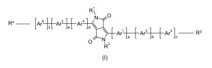
The invention relates especially to diketopyrrolopyrrol derivatives of the
formula I
R1
N 0
R4 [Ar6] t L Ar5 Je L Ar4 d
Ar'~--~ArAr3 ]C R3
O N
R2
(I)
CA 02700713 2010-03-25
WO 2009/047104 PCT/EP2008/062586
3
wherein R1 and R2 are independently of each other an aliphatic,
cycloaliphatic, cycloaliphatic-
aliphatic, aromatic, aromatic-aliphatic, heteroaromatic or heteroaromatic-
aliphatic group
having up to 49 carbon atoms,
a and d independently of each other are 0, 1, 2 or 3,
Ar1 and Ar4 are independently of each other a bivalent group of the formula II
or IV
(RS)p R6 R7
S
it I
(II) (IV)
wherein
R6 and R' are as defined below,
p represents 0, 1, or 2,
R5 is an aliphatic hydrocarbon group having up to 25 carbon atoms, or two
vicinal groups R5
together represent alkylene or alkenylene having up to 7 carbon atoms, it
being possible that
two groups R5 present in the group of formula II differ from each other,
b, c, e, and f independently of each other represent 1, 2 or 3,
Ar2 , Ar3 , Ar5 , and Ar6 are independently of each other a bivalent group of
one of the
formulae IV to X and L,
R6 R7 R$~ N S/ S/ R14 S
~ I II R9 R1z R15
S S R1o R11 R13 S R16
(IV) (V) (VI) (VII) (VIII)
R19 R2o
S S N~S~N
S
R17 S R1s R21
(IX) (X) (L)
wherein R6 , R' , R8, R9 , R12 , R13 R15 R 16 R17 , R18, R19, R20 and R21 are
independently
of each other hydrogen, C1-C25alkyl, C1-C18alkoxy, C6-C24aryl, C7-C25aralkyl,
or heteroaryl, or
R6 and R' together represent alkylene or alkenylene which may be both bonded
via oxygen
and/or sulfur to the thienyl residue and which may both have up to 25 carbon
atoms,
CA 02700713 2010-03-25
WO 2009/047104 PCT/EP2008/062586
4
R10 and R" are independently of each other hydrogen, C,-C,salkyl, C6-C24aryl,
heteroaryl, or
R10 and R" together represent oxo or form a five or six membered ring, which
is
unsubstituted or substituted by
a) an aliphatic hydrocarbon group having up to 18 carbon atoms,
b) C,-C,salkoxy or C2-C,salkylenedioxy in both of which carbon atoms which are
not adjacent
to oxygen may be replaced by oxygen, or
c) C6-C24aryl, C7-C25aralkyl, heteroaryl, C3-C,2cycloalkyl or C4-C,2cycloalkyl-
alkyl, and
R3 and R4 are independently of each other a group of one of the formulae XI to
XIX,
R24 R33 S R40 R39
R25 23 S
I R R2E R27 \ / \ R32 \ / \ \ R38
R34
R26 R22 I I R29 31 35 37
S R5a R3o R R R36 R
(XI) (XII) (XIII) (XIV)
R54 R54
R46 R46 R55 R53 R55 R53
R47 R45 47 R45 R56 R52 R56 R52
41
R44 R R44 R51 R57 R51
R41 R43 R43 R48 R50 R50
R42 R42 R49 R49
(XV) (XVI) (XVI I) (XVI 11)
R54
R55 R53
I R52
R57 R51
R48 R50
R49
(XIX)
wherein R22 to R26 and R29 to R58 represent independently of each other
hydrogen, an
aliphatic hydrocarbon group having up to 25 carbon atoms, alkoxy or alkenyloxy
having up to
18 carbon atoms, halogen, a cycloaliphatic, cycloaliphatic-aliphatic,
aromatic, aromatic-
aliphatic, heteroaromatic or heteroaromatic-aliphatic group having up to 25
carbon atoms, or
a group of the formula (III)
CA 02700713 2010-03-25
WO 2009/047104 PCT/EP2008/062586
PR3
= Pt
P R3
(III)
wherein R represents an aliphatic hydrocarbon group having up to 12 carbon
atoms, or two
5 groups R22 to R26 and R29 to R57 which are in the neighborhood of each
other, together
represent alkylene or alkenylene having up to 8 carbon atoms, thereby forming
a ring, and
R27 and R28 are independently of each other hydrogen, C,-C25alkyl, C,-
C,$alkoxy, C6-C24aryl,
C7-C25aralkyl, heteroaryl, or a group of the formula (III) shown above,
wherein R represents
an aliphatic hydrocarbon group having up to 12 carbon atoms, or R27 and R28
together or R27
and R58 together represent alkylene or alkenylene which may be both bonded via
oxygen
and/or sulfur to the thienyl residue and which may both have up to 25 carbon
atoms.
The general terms used above have the following meanings:
An aliphatic group having up to 49 carbon atoms, as represented e.g. by the
substituents R'
and R2, is an unsubstituted or substituted aliphatic hydrocarbon group having
up to 49, e.g.
up to 25 carbon atoms wherein the free valency extends from a carbon atom.
Preferably,
aliphatic groups as represented by the substituents R' and R2 have at least 7,
more
preferably at least 8, even more preferably at least 10, and most preferably
at least 14
carbon atoms. An aliphatic hydrocarbon group having up to 49, e.g. up to 25
carbon atoms is
a linear or branched alkyl, alkenyl or alkynyl (also spelled alkinyl) group
having up to 49, e.g.
up to 25 carbon atoms. Preferred are aliphatic hydrocarbon groups, like
especially alkyl
groups, having 7-49, especially 8-49, e.g. 7-25, especially 8-25, preferably
14-25 carbon
atoms. An example of a preferred alkyl group, as represented by the
substituents R' and R2,
is 2-decyl-tetradecyl.
Examples for C,-C25alkyl groups are methyl, ethyl, n-propyl, isopropyl, n-
butyl, sec.-butyl,
isobutyl, tert.-butyl, n-pentyl, 2-pentyl, 3-pentyl, 2,2-dimethylpropyl,
1,1,3,3-tetramethylpentyl,
n-hexyl, 1-methylhexyl, 1,1,3,3,5,5-hexamethylhexyl, n-heptyl, isoheptyl,
1,1,3,3-
tetramethylbutyl, 1-methylheptyl, 3-methylheptyl, n-octyl, 3,7-dimethyl-octyl,
1,1,3,3-
tetramethylbutyl, 2-ethylhexyl, 2-n-butyl-hexyl, n-nonyl, decyl, 2-hexyl-
decyl, undecyl,
dodecyl, tridecyl, tetradecyl, 2-decyl-tetradecyl, pentadecyl, hexadecyl,
heptadecyl,
octadecyl, eicosyl, heneicosyl, docosyl, tetracosyl and pentacosyl, of which 2-
decyl-
tetradecyl is especially preferred as a meaning of R' and R2.
CA 02700713 2010-03-25
WO 2009/047104 PCT/EP2008/062586
6
Examples for C2-C25alkenyl groups are vinyl, allyl, methallyl, isopropenyl, 2-
butenyl, 3-
butenyl, isobutenyl, n-penta-2,4-dienyl, 3-methyl-but-2-enyl, n-oct-2-enyl, n-
dodec-2-enyl,
isododecenyl, n-dodec-2-enyl or n-octadec-4-enyl.
Examples for C2_25alkynyl groups are ethynyl, 1-propyn-3-yl, 1-butyn-4-yl, 1-
pentyn-5-yl,
2-methyl-3-butyn-2-yl, 1,4-pentadiyn-3-yl, 1,3-pentadiyn-5-yl, 1-hexyn-6-yl,
cis-3-methyl-2-
penten-4-yn-1-yl, trans-3-methyl-2-penten-4-yn-1-yl, 1,3-hexadiyn-5-yl, 1-
octyn-8-yl,
1-nonyn-9-yl, 1-decyn-10-yl, or 1-tetracosyn-24-yl.
Aliphatic groups can, in contrast to aliphatic hydrocarbon groups, be
substituted by any
acyclic substituents, but are preferably unsubstituted. Preferred substituents
are C,-C$alkoxy
or C,-C$alkylthio groups as exemplified further below. The term "aliphatic
group" comprises
also alkyl groups wherein certain non-adjacent carbon atoms are replaced by
oxygen, like
-CH2-O-CH2-CH2-O-CH3. The latter group can be regarded as methyl substituted
by -O-CH2-
CH2-O-CH3.
A cycloaliphatic group having up to 49, e.g. up to 25 carbon atoms, as
represented e.g. by
the substituents R' and R2, is an unsubstituted or substituted cycloaliphatic
hydrocarbon
group having up to 49, e.g. up to 25 carbon atoms wherein the free valency
extends from a
ring carbon atom.
A cycloaliphatic hydrocarbon group is a cycloalkyl or cycloalkenyl group which
may be
substituted by one or more aliphatic and/or cycloaliphatic hydrocarbon groups.
A cycloalkyl group has at least 3, preferably at least 5 carbon atoms and is
typically C5-
C1zcycloalkyl, such as cyclopentyl, cyclohexyl, cycloheptyl, cyclooctyl,
cyclononyl, cyclodecyl,
cycloundecyl, cyclododecyl, preferably cyclopentyl, cyclohexyl, cycloheptyl,
or cyclooctyl,
which may be unsubstituted or substituted by one or more aliphatic and/or
cycloaliphatic
hydrocarbon groups and/or condensed with phenyl groups as defined herein
and/or
condensed with phenyl groups.
A cycloaliphatic-aliphatic group is an aliphatic group substituted by a
cycloaliphatic group,
wherein the terms "cycloaliphatic" and "aliphatic" have the meanings given
herein and
wherein the free valency extends from the aliphatic moiety. Hence, a
cycloaliphatic-aliphatic
group is for example a cycloalkyl-alkyl group.
CA 02700713 2010-03-25
WO 2009/047104 PCT/EP2008/062586
7
A cycloalkyl-alkyl group is an alkyl group substituted by a cycloalkyl group,
e.g.
cyclohexyl-methyl.
A "cycloalkenyl group" means an unsaturated alicyclic hydrocarbon group
containing one or
more double bonds, such as cyclopentenyl, cyclopentadienyl, cyclohexenyl and
the like,
which may be unsubstituted or substituted by one or more aliphatic and/or
cycloaliphatic
hydrocarbon groups and/or condensed with phenyl groups.
For example, a cycloalkyl or cycloalkenyl group, in particular a cyclohexyl
group, can be
condensed one or two times with phenyl which can be substituted one to three
times with C,-
C4-alkyl. Examples of such condensed cyclohexyl groups are groups of the
formulae XX to
XXIV:
or
(XX) (XXI) (XXI 1)
/
in particular or ,
(XXIII) (XXIV)
which can be substituted in the phenyl moieties one to three times with C,-C4-
alkyl.
Preferred substituents of a substituted cycloaliphatic hydrocarbon group are
e.g. C,-C$alkoxy
or C,-C$alkylthio groups.
Preferably, a and d, independently of each other, are 0, 1 or 2. Also
preferably a and d have
the same meaning.
An aliphatic hydrocarbon group having up to 25 carbon atoms R5 is a linear or
branched
alkyl, alkenyl or alkynyl (also spelled alkinyl) group having up to 25 carbon
atoms as
exemplified above.
CA 02700713 2010-03-25
WO 2009/047104 PCT/EP2008/062586
8
Alkylene is bivalent alkyl, i.e. alkyl having two (instead of one) free
valencies, e.g.
trimethylene or tetramethylene.
Alkenylene is bivalent alkenyl, i.e. alkenyl having two (instead of one) free
valencies, e.g.
-CH2-CH=CH-CH2-.
A bivalent group of the formula II wherein two vicinal groups R5 together
represent alkylene
or alkenylene having up to 7 carbon atoms, it being possible that two groups
R5 present in
the group of formula II differ from each other, is for example a group of the
formula
\ \ \ \
or or or
(XXV) (XXVI) (xxvI I ) (xxvI I I )
C1-C25alkyl as represented by R6 , R' , R8, R9, R12 , R13 , R15 R1s R17 , R18,
R19, R20 and
R21 has the meanings given above.
C1-C18alkoxy, as represented e.g. by R6 , R' , R8, R9 , R12 , R13 , R15 R1s
R17 R18, R19,
R20 and R21 to R26, is e.g. methoxy, ethoxy, n-propoxy, isopropoxy, n-butoxy,
sec.-butoxy,
isobutoxy, tert.-butoxy, n-pentoxy, 2-pentoxy, 3-pentoxy, 2,2-dimethylpropoxy,
n-hexoxy, n-
heptoxy, n-octoxy, 1,1,3,3-tetramethylbutoxy, 2-ethylhexoxy, n-nonoxy, decoxy,
undecoxy,
dodecoxy, tridecoxy, tetradecoxy, pentadecoxy, hexadecoxy, heptadecoxy, and
octadecoxy,
preferably C1-C4alkoxy.
The term "alkylthio group" means the same groups as the alkoxy groups, except
that the
oxygen atom of ether linkage is replaced by a sulfur atom.
An aromatic group as represented e.g. by R1 and R2 is preferably C6-C24aryl.
C6-C24aryl, as represented e.g. by R1, R2 , R6 , R' , R8, R9 , R12 , R13 , R15
R1s R17 R18, R19
, R20 and R21 , is e.g. substituted or preferably unsubstituted phenyl,
indenyl, azulenyl,
naphthyl, biphenyl, as-indacenyl, s-indacenyl, acenaphthylenyl, fluorenyl,
phenanthryl,
fluoranthenyl, triphenlenyl, chrysenyl, naphthacen, picenyl, perylenyl,
pentaphenyl,
hexacenyl, pyrenyl, or anthracenyl, preferably phenyl, 1-naphthyl, 2-naphthyl,
3- or
CA 02700713 2010-03-25
WO 2009/047104 PCT/EP2008/062586
9
4-biphenyl, 9-phenanthryl, 2- or 9-fluorenyl, 3- or 4-biphenyl, which all may
be unsubstituted
or substituted, e.g. by alkyl or alkoxy.
An aromatic-aliphatic group as represented e.g. by R1 and R2 is an aliphatic
group which is
substituted by an aromatic group, wherein the terms "aromatic" and "aliphatic"
are as
defined herein, e.g. an aralkyl group, like 3-phenyl-propyl.
C7-C25aralkyl, as represented e.g. by R6 , R' , R8, R9 , R12 , R13 , R15 R1s
R17 R18, R19,
R20 , R21, R27, or R28 is e.g. phenyl-alkyl, like benzyl, 2-benzyl-2-propyl, R-
phenyl-ethyl,
a,a-dimethylbenzyl, 3-phenyl-propyl, cjrphenyl-butyl, w,c,rdimethyl-c,rphenyl-
butyl, cjrphenyl-
dodecyl, cirphenyl-octadecyl, cjrphenyl-eicosyl, and cirphenyl-docosyl,
wherein the phenyl
moiety may be unsubstituted or substituted, e.g. by alkyl, alkoxy or halogen.
A preferred
meaning for C7-C25aralkyl, as represented by R6 , R' , R27, or R28 is e.g. 3-
phenyl-propyl.
A heteroaromatic group having up to 49, preferably up to 25 carbon atoms as
represented
e.g. by R1 and R2 is a heteroaryl group as defined below, but not having more
than 49,
preferably not more than 25 carbon atoms.
Heteroaryl, as represented e.g. by R6 , R' , R8, R9, R12 , R13 , R15 R16 R17
R18, R19, R20
and R21, is e.g. C2_C26heteroaryl, i.e. e.g. a ring with five to seven ring
atoms or a condensed
ring system, wherein nitrogen, oxygen or sulfur are the possible hetero atoms,
and is
typically an unsaturated heterocyclic group with five to 30 atoms (including
both carbon and
hetero atoms) having at least six conjugated Tc-electrons, such as thienyl,
benzo[b]thienyl,
dibenzo[b,d]thienyl, thianthrenyl, furyl, furfuryl, 2H-pyranyl, benzofuranyl,
isobenzofuranyl,
dibenzofuranyl, phenoxythienyl, pyrrolyl, imidazolyl, pyrazolyl, pyridyl,
bipyridyl, triazinyl,
pyrimidinyl, pyrazinyl, pyridazinyl, indolizinyl, isoindolyl, indolyl,
indazolyl, purinyl, quinolizinyl,
chinolyl, isochinolyl, phthalazinyl, naphthyridinyl, chinoxalinyl,
chinazolinyl, cinnolinyl,
pteridinyl, carbazolyl, carbolinyl, benzotriazolyl, benzoxazolyl,
phenanthridinyl, acridinyl,
pyrimidinyl, phenanthrolinyl, phenazinyl, isothiazolyl, phenothiazinyl,
isoxazolyl, furazanyl or
phenoxazinyl, which can be unsubstituted or substituted, e.g. by alkyl.
A heteroaromatic-aliphatic group having up to 49, preferably up to 25 carbon
atoms as
represented e.g. by R1 and R2 is an aliphatic group substituted by an
heteroaromatic group
wherein the terms "aliphatic" and "heteroaromatic" are as defined herein
except for the total
number of carbon atoms which must not exceed 49, preferably 25, and wherein
the free
valency extends from the aliphatic moiety, e.g. heteroaryl-methyl.
CA 02700713 2010-03-25
WO 2009/047104 PCT/EP2008/062586
A bivalent group of the formula IV wherein R6 and R' together represent
alkylene or
alkenylene which may be both bonded via oxygen and/or sulfur to the thienyl
residue and
which may both have up to 25 carbon atoms, is e.g. a group of the formula XXIX
or XXX
5
Y~A\O
Y
S or S
(XXIX) (XXX)
wherein A represents linear or branched alkylene having up to 25 carbon atoms,
preferably
ethylene or propylene which may be substituted by one or more alkyl groups,
and Y
10 represents oxygen or sulphur. For example, the bivalent group of the
formula -Y-A-O-
represents -O-CHz-CHz-O- or -O-CHz-CHz-CHz-O- .
A bivalent group of the formula VI wherein R10 and R" together represent oxo
is a group of
the formula (XXXI).
S S
~ ~ ~ ~
Rs R~z
O
(XXXI)
C,-C,$alkoxy in which carbon atoms which are not adjacent to oxygen may be
replaced by
oxygen is e.g. a group of one of the formulae -O-CH2-O-CH2-CH2-O-CH3,
-O-(CH2)20CH3, -O-(CH2CH2O)2CH2CH3, -O-CH2-O-CH3, -O-CH2CH2-O-CH2CH3,
-O-CH2CH2CH2-O-CH(CH3)2, -O-[CH2CH2O]n-CH3 wherein n = 1-10,
-O-CH2-CH(CH3)-O-CH2-CH2CH3 and -O-CH2-CH(CH3)-O-CH2-CH3.
Cz-C,$alkylenedioxy in which carbon atoms which are not adjacent to oxygen may
be
replaced by oxygen is e.g. a group of the formula -O-CHz-O-CHz-CHz-O-.
An aliphatic, cycloaliphatic, cycloaliphatic-aliphatic, aromatic, aromatic-
aliphatic,
heteroaromatic or heteroaromatic-aliphatic group having up to 25 carbon atoms
as
CA 02700713 2010-03-25
WO 2009/047104 PCT/EP2008/062586
11
substituent R22 to R26 of a group of the formula XI has the meanings defined
above. A
preferred group of the formula XI is the 4-biphenyl group, which may be
unsubstituted or
substituted within the scope of the above terms.
An example for alkenyloxy is e.g. 3-butenyloxy.
Halogen is fluoro, chloro, bromo or iodo.
A group of the formula XI wherein two groups R22 to R26 which are in the
neighborhood of
each other, together represent alkylene or alkenylene having up to 8 carbon
atoms, thereby
forming a ring, is e.g. a group of the formula XXXII or XXXIII
i i
(XXXI I ) (XXXI I I )
wherein in the group of the formula XXXII R23 and R24 together represent 1,4-
butylene and
wherein in the group of the formula XXXIII R23 and R24 together represent 1,4-
but-2-en-ylene.
A group of the formula XI I, wherein R27 and R28 together represent alkylene
or alkenylene
which may be both bonded via oxygen and/or sulfur to the thienyl residue and
which may
both have up to 25 carbon atoms, is e.g. a group of the formula XXXIV or XXXV
A~O Y
R5s R58
(XXXIV) (XXXV)
wherein A represents linear or branched alkylene having up to 25 carbon atoms,
preferably
ethylene or propylene which may be substituted by one or more alkyl groups,
and Y
represents oxygen or sulphur. For example, the bivalent group of the formula -
Y-A-O-
represents -O-CH2-CH2-O- or -O-CH2-CH2-CH2-O- .
CA 02700713 2010-03-25
WO 2009/047104 PCT/EP2008/062586
12
Preferred are compounds of the formula I wherein R' and R2 are independently
of each other
an aliphatic, cycloaliphatic, cycloaliphatic-aliphatic, aromatic, aromatic-
aliphatic,
heteroaromatic or heteroaromatic-aliphatic group having up to 25 carbon atoms,
R3 and R4 are independently of each other a group of one of the formulae XI to
XIX,
R24 R33 S R40 R39
R25 23 S
I R R2E R27 \ / \ R32 \ / \ \ R38
R34
R26 R22 I I R29 31 35 37
S R5a R3o R R R36 R
(Xl) (XII) (XIII) (XIV)
R54 R54
R46 R46 R55 R53 R55 R53
R47 R45 47 R45 R56 R52 R56 R52
41
R44 R R44 R51 R57 R51
R41 R43 R43 R48 R50 R50
R42 R42 R49 R49
(XV) (XVI) (XVI I) (XVI 11)
R54
R55 R53
I R52
R57 R51
R48 R50
R49
(XIX)
wherein R22 to R26 and R29 to R58 represent independently of each other
hydrogen, an
aliphatic hydrocarbon group having up to 25 carbon atoms, or a group of the
formula (III)
PR3
= Pt
P R3
(III)
CA 02700713 2010-03-25
WO 2009/047104 PCT/EP2008/062586
13
wherein R represents an aliphatic hydrocarbon group having up to 12 carbon
atoms, or two
groups R22 to R26 and R29 to R57 which are in the neighborhood of each other,
together
represent alkylene or alkenylene having up to 8 carbon atoms, thereby forming
a ring, and
R27 and R28 are independently of each other hydrogen, C,-C25alkyl, C,-
C,$alkoxy, C6-C24aryl,
C7-C25aralkyl, heteroaryl, or a group of the formula (III) shown above,
wherein R represents
an aliphatic hydrocarbon group having up to 12 carbon atoms, or R27 and R28
together or R27
and R58 together represent alkylene or alkenylene which may be both bonded via
oxygen
and/or sulfur to the thienyl residue and which may both have up to 25 carbon
atoms, and the
remaining substituents have the meanings given above.
Especially preferred are compounds of the formula I wherein R' and R2 are
independently of
each other an aliphatic, cycloaliphatic or cycloaliphatic-aliphatic
hydrocarbon group having
up to 25 carbon atoms,
a and d represent 0,
b, c, e, and f represent 1,
Ar2 , Ar3 , Ar5 , and Ar6 are independently of each other a bivalent group of
the formula IV,
R6 R7
S
it I
(IV)
wherein R6 and R' are independently of each other hydrogen or C,-C25alkyl, and
R3 and R4 are independently of each other a group of the formula
R28 R27
t S'R58
(XII)
wherein R58 represents hydrogen or an aliphatic hydrocarbon group having up to
25 carbon
atoms, and
R27 and R28 are independently of each other hydrogen or C,-C25alkyl.
More especially preferred are compounds of the formula I wherein R' and R2 are
independently of each other an aliphatic, cycloaliphatic or cycloaliphatic-
aliphatic
hydrocarbon group having up to 25 carbon atoms,
a and d represent 0,
b, c, e, and f represent 1,
Ar2 and Ar5 are independently of each other a bivalent group of the formula
IV,
CA 02700713 2010-03-25
WO 2009/047104 PCT/EP2008/062586
14
R6 R7
S
it
(IV)
wherein one of R6 and R' represents C,-C25alkyl while the other of R6 and R'
represents
hydrogen or C,-C25alkyl,
Ar3 and Ar6 are a bivalent group of the formula IV, wherein each of R6 and
R'represents
hydrogen, and
R3 and R4 are independently of each other a group of the formula
R28 R27
t S'R58
(XII)
wherein R58 represents hydrogen or an aliphatic hydrocarbon group having up to
25 carbon
atoms, and
one of R27 and R28 represents C,-C25alkyl while the other of R27 and R28
represents hydrogen
or C,-C25alkyl.
Very preferred are compounds of the formula I wherein
R' and R2 are independently of each other an alkyl group having up to 49
carbon atoms,
a and d are independently of each other 0, 1 or 2,
Ar' and Ar4 are independently of each other a bivalent group of the formula IV
R6 R7
S
it
(IV)
wherein
R6 and R' are independently of each other hydrogen or C,-C25alkyl,
b, c, e, and f independently of each other represent 1, 2 or 3
Ar2 , Ar3 , Ar5 , and Ar6 are independently of each other a bivalent group of
the formula IV,
R6 R7
S
it
(IV)
CA 02700713 2010-03-25
WO 2009/047104 PCT/EP2008/062586
wherein R6 and R7 are independently of each other hydrogen, C,-C25alkyl, or C7-
C25aralkyl,
and
R3 and R4 are independently of each other a group of one of the formulae XI to
XIII, XV, XVI
and XIX
R24 R33
R23 S
R28 R27 R32
R26 R22 I I R31
S R5a R3o R
5
(XI) (XII) (XIII)
R54
R46 R46 R55 R53
R47 R45 47 R45 R 52
41
R44 R R44 R57 R51
R41 R43 R43 p48 R50
R42 R42 R R49
(XV) (XVI) (XIX)
10 wherein R22 to R26 , R29 to R33 , R41 to R55 , R57 and R58 represent
independently of each
other hydrogen, an aliphatic hydrocarbon group having up to 25 carbon atoms,
aryl, alkoxy
having up to 18 carbon atoms, or halogen, or two groups R22 to R26 which are
in the
neighborhood of each other, together represent alkylene or alkenylene having
up to 8 carbon
atoms, thereby forming a ring, and
15 R27 and R28 are independently of each other hydrogen, C,-C25alkyl, or C7-
C25aralkyl, or R27
and R28 together represent alkylene or alkenylene which may be both bonded via
oxygen
and/or sulfur to the thienyl residue and which may both have up to 25 carbon
atoms.
Very preferred are especially the above-mentioned compounds of the formula I
wherein R'
20 and R2 have the same meaning and the side chains of the formulae XLV and
XLVI are
identical to each other.
f_Ar1 Ja L Ar2 Ja L Ar3 Ic R3 R4 [Ar6 Jf L Ar5 Je L Ar4 Jd
(XLV) (XLVI)
25 Most preferred are the compounds of the formula I described in the
Examples, especially a
compound of the general formula I selected from the compounds having the
formulae 13, 22,
CA 02700713 2010-03-25
WO 2009/047104 PCT/EP2008/062586
16
23, 24, 25, 26, 32, 38, 44, 45, 50, 55, 56, 58, 59, 60, 61, 63, 64, 70, 74,
76, 78, 80, 81, 82,
83, 84, 85, 86, 87, 88 and 89, respectively, which are depicted in the
Examples.
The compounds of the formula I can be manufactured by known methods.
A possible route of manufacture starts from a compound of the formula XXXIV
H
4 d
N [Ar
Ar' H
O N
H
(XXXIV)
wherein a and d represent 1 and Ar' and Ar4 have the meanings given above, or
from a
compound of the formula XXXV
H
N O
H+Ar+~Ar4 d
[ArH
O N
H
(XXXV)
wherein a and d represent 0, b and e represent 1, and Ar2 and Ar5 have the
meanings given
above.
Said starting compounds of the formulae XXXIV and XXXV can be obtained as
described in
US patent 4,579,949 by reacting (in the presence of a strong base) one mole of
a
disuccinate, like dimethyl succinate, with 1 mole of a nitrile of the formulae
XXXVI or XXXVII
H-Ar'-CN (XXXVI) H-Ar4-CN (XXXVII)
and 1 mole of a nitrile of the formulae XXXVIII or XXXIX.
H-Ar2-CN (XXXVIII) H-Ar5-CN (XXXIX)
Alternatively, said starting compounds of the formulae XXXIV and XXXV can be
obtained as
described in US patent 4,659,775 by reacting a nitrile with a suitable ester,
like a pyrrolinon-
3-carboxylic ester derivative.
CA 02700713 2010-03-25
WO 2009/047104 PCT/EP2008/062586
17
The thus obtained compound of the formula XXXIV or the thus obtained compound
of the
formula XXXV is then N-alkylated for introduction of the groups R' and R2,
e.g. by reaction
with a bromide of the formula R1-Br or R2-Br in the presence of a suitable
base, like
potassium carbonate, in a suitable solvent, like N-methyl-pyrrolidone. The
reaction is carried
out at a temperature from about room temperature to about 180 C, preferably
from about
100 C to about 170 C, e.g. at 140 C.
The thus obtained compound of the formula XL
R1
N O
H~-f Ar4 d
Ar'~
O N a
R2
(XL)
wherein a and d represent 1, and R' , R2 , Ar' and Ar4 have the meanings given
above,
or the thus obtained compound of the formula XLI
R1
O
N
H+Ar+~Ar4 d
[ArH
O N
R2
(XLI)
wherein a and d represent 0, b and e represent 1, and R' , R2 , Ar2 and Ar5
have the
meanings given above, is then reacted with a suitable brominating agent, like
N-bromo-
succinimide, to yield a compound of the formulae XLII and XLIII, respectively.
R R
N O N O
Br+ -Ar4 d ]e[ Ar4 d
N Ar'~Br N Ar'~--~Ar~Br
O R2 O R2
(XLII) (XLIII)
CA 02700713 2010-03-25
WO 2009/047104 PCT/EP2008/062586
18
The bromination is carried out in a suitable solvent, like chloroform, using
two equivalents of
N-bromo-succinimide at a temperature between -30 C and +50 C, preferably
between -10 C
and room temperature, e.g. at 0 C.
The compounds of the formulae XLII or XLIII can then be "side-chain-
elongated", by step-
wise adding further groups Ar'-H, Ar4-H, Ar2-H, Ar5-H, Ar3-R3 , and Ar6-R4.
The step-wise
addition of these groups can be effected e.g. by reacting a compound of the
formulae XLII or
XLIII with a suitable tin compound of the formula XLIV
(R59)3Sn-Ar1-6 (XLIV)
wherein R59 represents C1_7alkyl, like butyl, and Ar1-6 represents Ar'-H, Ar4-
H, Ar2-H, Ar5-H,
Ar3-R3 , or Ar6-R4, respectively.
The reaction is carried out in the presence of a suitable palladium catalyst,
like Pd(P[C6H5]3)4
, in a suitable solvent, e.g. an aromatic hydrocarbon solvent, like toluene,
at a temperature
between about 50 C and 180 C, e.g. under reflux, and under inert conditions
including, inter
alia, the use of dry solvents. After cooling down, the reaction mixture may be
e.g. filtrated,
e.g. on a double layer silica gel/Hyflo , concentrated and the desired
compound precipitated,
e.g. by addition of methanol.
The "side-chain-elongation" of the compounds of the formulae XLII or XLIII
with an additional
thienyl residue can also be effected e.g. by reaction with a mixture of 2-
thienylboronic acid
pinacol ester, Pd2(dba)3 [tris(dibenzylideneacetone)-di-palladium)] and tri-
tert-butyl-
phosphonium-tetrafluoroborate in tetrahydrofurane.
The 2-thienylboronic acid pinacol ester may be obtained e.g. by adding
substituted or
unsubstituted thiophene to a mixture prepared from n-butyl-lithium and
diisopropylamine and
by adding 2-isopropoxy-4,4,5,5-tetramethyl-1,3,2-dioxaborolane to the thus
obtained mixture.
Analogously, the "side-chain-elongation" of the compounds of the formulae XLII
or XLIII with
an additional phenyl or biphenyl residue may be effected with phenyl-boronic
acid pinacol
ester or biphenyl-boronic acid pinacol ester.
Alternatively, for the manufacture of compounds of the formula I wherein the
side chains of
the formulae XLV and XLVI
CA 02700713 2010-03-25
WO 2009/047104 PCT/EP2008/062586
19
+Ar1 Ja L ArZ Ja L Ar3 Ic R3 R4 [Ar6 Jf L Ar5 Je L Ar4 Jd
(XLV) (XLVI)
are identical to each other, it is also possible to build up the complete side
chains first and
then reacting a nitrile of the formula XLVII
R4 [Ar6 Jf L Ar5 Je L Ar4dCN
(XLVI I )
with a suitable disuccinate, e.g. di-tert-amyl succinate. For example, a
mixture of iron(III)-
chloride (FeCl3), sodium, and tert-amylalcohol may be heated to 60-160 C, e.g.
110 C,
before a mixture of the nitrile of the formula XLVII and di-tert-amyl
succinate is added drop
wise. After stirring the reaction mixture until the reaction is complete, e.g.
for about 19 hours
at 110 C, the reaction mixture is poured onto a water-methanol mixture.
Compounds of the formulae XLVa and XLVIa containing the complete side chains
can be
H~Ar'~--~Ar2 J n L Ar3 I c R3 R4 [Ar6 1 [ Ar5 le [ Ar4 H
(XLVa) (XLVIa)
manufactured e.g. by reacting a bromo derivative of the formula Br-Ar' etc.
first with
magnesium in diethyl ether and then adding the thus obtained Grignard solution
to a solution
in diethyl ether of Ni(dppp)C12 and a mono- or, if desired, dibromo compound
of the formula
Br-Ar2 or Br-Ar2T-Br, respectively.
The conversion of a compound of the formula XLVIa into the nitrile of the
formula XLVII may
be effected e.g. by adding a solution of a compound of the formula XLVIa, e.g.
in toluene, to
the reaction mixture obtained by adding triflic anhydride to a solution of N-
formylmethylaniline
in e.g. toluene, and reacting the obtained aldehyde of the formula XLVIIa
H
R4 [Ar6 ~Ar~--~Ar4
f e d
0
(XLVIIa)
with hydroxylamine sulfate in e.g. dimethyl formamide.
CA 02700713 2010-03-25
WO 2009/047104 PCT/EP2008/062586
The thus obtained compound of the formula I wherein R' and R2 are hydrogen may
then be
transformed into a desired end product of the formula I wherein R' and R2 are
e.g. an
aliphatic, cycloaliphatic, cycloaliphatic-aliphatic, or aromatic-aliphatic
group, like especially
such an hydrocarbon group, by N-alkylation, e.g. analogously as described
above, or by
5 heating a solution thereof and potassium carbonate in dimethyl formamide
followed by
addition of R1-Br or R2-Br, or by reaction with a suitable iodide of the
formula R'-I or R2-I.
For example, a mixture of a compound of the formula I wherein R' and R2 are
hydrogen in N-
methyl-pyrrolidone is treated, preferably under cooling, e.g. to a temperature
between about
0 C and 10 C, e.g. about 5 C, with a suitable strong base, e.g. a suitable
hydride, like an
10 alkali metal hydride, e.g. sodium hydride. Thereafter, the iodide of the
formula R'-I or R2-1 is
added.
The nitrile of the formula XLVII used as starting material may be prepared
e.g. from the
corresponding aldehyde of the formula XLVIII,
R4 [Ar6][ Ar5 Je L Ar4dCHO
(XLVIII)
e.g. by reaction with hydroxylamine.
Said aldehyde of the formula XLVIII may be prepared e.g. from a compound of
the formula
I L,
R4 [Ar6 Jf L Ar5 Je FArqH
(IL)
e.g. by adding a solution of a compound of the formula IL in a suitable
solvent, like toluene,
to the reaction mixture of N-formylmethylaniline in a suitable solvent, like
toluene, and triflic
anhydride.
The present invention relates also to new starting materials, especially to
compounds of the
formula I wherein one or both of R' and R2 are hydrogen, prefererably to such
compounds
which, like the end products of the formula I can also be used as the
semiconductor layer in
semiconductor devices. Preferred are those starting materials of the formula I
wherein one or
both of R' and R2 are hydrogen and which contain at least two or three Ar
groups in each
side chain.
CA 02700713 2010-03-25
WO 2009/047104 PCT/EP2008/062586
21
The compounds of the formula I show clear p-type transistor behavior and can
be used as
the semiconductor layer in semiconductor devices. Accordingly, the present
invention also
relates to a semiconductor device comprising as a semiconducting effective
means a
compound of the formula I
R1
N 0
R4 [Ar6] t L Ar5 Je L Ar4 d
Ar'~--~ArAr3 ]C R3
O N
R2
(I)
wherein R' and R2 are independently of each other an aliphatic group having 7
to 25 carbon
atoms, or a cycloaliphatic, cycloaliphatic-aliphatic, aromatic, aromatic
aliphatic,
heteroaromatic or heteroaromatic-aliphatic group having up to 25 carbon atoms,
a and d independently of each other are 0, 1, 2 or 3,
Ar' and Ar4 are independently of each other a bivalent group of the formula II
or IV
(RS)p R6 R7
S
it I
(II) (IV)
wherein
R6 and R' are as defined below,
p represents 0, 1, or 2,
R5 is an aliphatic hydrocarbon group having up to 25 carbon atoms, or two
vicinal groups R5
together represent alkylene or alkenylene having up to 7 carbon atoms, it
being possible that
two groups R5 present in the group of formula I I differ from each other,
b and e independently of each other represent 1, 2 or 3,
c and f independently of each other represent 0, 1, 2 or 3,
Ar2 , Ar3 , Ar5 , and Ar6 are independently of each other a bivalent group of
one of the
formulae IV to X and L,
R6 R7 R$~ N S/ S/ R14 S
~ I II R9 R~z R15
S S R1o R11 R13 S R16
(IV) (V) (VI) (VII) (VIII)
CA 02700713 2010-03-25
WO 2009/047104 PCT/EP2008/062586
22
R19 R20
S S N~S~N
~ ~ Z S I / /
R17 S R1s R21
(IX) (X) (L)
wherein R6 , R7 , R8, R9, R12 , R13 , R15 R1s R17 , R18, R19, R20 and R21 are
independently
of each other hydrogen, C1-C25alkyl, C1-C18alkoxy, C6-C24aryl, C7-C25aralkyl,
or heteroaryl, or
R6 and R7 together represent alkylene or alkenylene which may be both bonded
via oxygen
and/or sulfur to the thienyl residue and which may both have up to 25 carbon
atoms,
R10 and R11 are independently of each other hydrogen, C1-C18alkyl, C6-C24aryl,
heteroaryl, or
R10 and R11 together represent oxo or form a five or six membered ring, which
is
unsubstituted or substituted by
a) an aliphatic hydrocarbon group having up to 18 carbon atoms,
b) C1-C18alkoxy or C2-C18alkylenedioxy in both of which carbon atoms which are
not adjacent
to oxygen may be replaced by oxygen, or
c) C6-C24aryl, C7-C25aralkyl, heteroaryl, C3-C12cycloalkyl or C4-C12cycloalkyl-
alkyl, and
R3 and R4 are independently of each other a group of one of the formulae XI to
XIX,
R24 R33 S R40 R39
R25 23 S
I R R2E R27 \ / \ R32 \ / \ \ R38
R34
R26 R22 I I R29 31 35 37
S R5a R3o R R R36 R
(X1) (XII) (XIII) (XIV)
R54 R54
R46 R46 R55 R53 R55 R53
R47 R45 47 R45 R56 R52 R56 R52
41
R44 R R44 R51 R57 R51
R41 R43 R43 R48 R50 R50
R42 R42 R49 R49
(XV) (XVI) (XVII) (XVI I I)
CA 02700713 2010-03-25
WO 2009/047104 PCT/EP2008/062586
23
R54
R55 R53
R5z
R57 R51
R48 R50
R49
(XIX)
wherein R22 to R26 and R29 to R58 represent independently of each other
hydrogen, an
aliphatic hydrocarbon group having up to 25 carbon atoms, or a group of the
formula (III)
PR3
= Pt
P R3
(III)
wherein R represents an aliphatic hydrocarbon group having up to 12 carbon
atoms, or two
groups R22 to R26 and R29 to R57 which are in the neighborhood of each other,
together
represent alkylene or alkenylene having up to 8 carbon atoms, thereby forming
a ring, and
R27 and R28 are independently of each other hydrogen, C,-C25alkyl, C,-
C,$alkoxy, C6-C24aryl,
C7-C25aralkyl, heteroaryl, or a group of the formula (III) shown above,
wherein R represents
an aliphatic hydrocarbon group having up to 12 carbon atoms, or R27 and R28
together or R27
and R58 together represent alkylene or alkenylene which may be both bonded via
oxygen
and/or sulfur to the thienyl residue and which may both have up to 25 carbon
atoms,
especially to a semiconductor device comprising as a semiconducting effective
means a
compound of the formula I as defined in this paragraph with the proviso that
at least one of
R6, R' , R27 , R28 and R58 is different from hydrogen.
The invention relates especially to a semiconductor device comprising as as a
semiconducting effective means a compound of the formula I described in the
Examples
selected from the compounds having the formulae 3, 16, 53, 67, 68, 69, 71, and
77,
respectively, which are depicted in the Examples.
Preferably, the invention relates to a semiconductor device comprising as as a
semiconducting effective means a compound of the general formula I selected
from the
compounds having the formulae 13, 22, 23, 24, 25, 26, 32, 38, 44, 45, 50, 55,
56, 58, 59, 60,
CA 02700713 2010-03-25
WO 2009/047104 PCT/EP2008/062586
24
61, 63, 64, 70, 74, 76, 78, 80, 81, 82, 83, 84, 85, 86, 87, 88, and 89,
respectively, which are
depicted in the Examples.
Preferably said semiconductor device is a diode, a photodiode, a sensor, an
organic field
effect transistor (OFET), a transistor for flexible displays, or a solar cell,
or a device
containing a diode and/or an organic field effect transistor, and/or a solar
cell. There are
numerous types of semiconductor devices. Common to all is the presence of one
or more
semiconductor materials. Semiconductor devices have been described, for
example, by S.
M. Sze in Physics of Semiconductor Devices, 2nd edition, John Wiley and Sons,
New York
(1981). Such devices include rectifiers, transistors (of which there are many
types, including
p-n-p, n-p-n, and thin-film transistors), light emitting semiconductor devices
(for example,
organic light emitting diodes in display applications or backlight in e.g.
liquid crystal displays),
photoconductors, current limiters, solar cells, thermistors, p-n junctions,
field-effect diodes,
Schottky diodes, and so forth. In each semiconductor device, the semiconductor
material is
combined with one or more metals and/or insulators to form the device.
Semiconductor
devices can be prepared or manufactured by known methods such as, for example,
those
described by Peter Van Zant in Microchip Fabrication, Fourth Edition, McGraw-
Hill, New York
(2000). In particular, organic electronic components can be manufactured as
described by
D.R. Gamota et al. in Printed Organic and Molecular Electronics, Kluver
Academic Publ.,
Boston, 2004.
A particularly useful type of transistor device, the thin-film transistor
(TFT), generally includes
a gate electrode, a gate dielectric on the gate electrode, a source electrode
and a drain
electrode adjacent to the gate dielectric, and a semiconductor layer adjacent
to the gate
dielectric and adjacent to the source and drain electrodes (see, for example,
S. M. Sze,
Physics of Semiconductor Devices, 2nd edition, John Wiley and Sons, page
492, New
York (1981)). These components can be assembled in a variety of
configurations. More
specifically, an organic thin-film transistor (OTFT) has an organic
semiconductor layer.
Typically, a substrate supports the OTFT during manufacturing, testing, and/or
use.
Optionally, the substrate can provide an electrical function for the OTFT.
Useful substrate
materials include organic and inorganic materials. For example, the substrate
can comprise
silicon materials inclusive of various appropriate forms of silicon, inorganic
glasses, ceramic
foils, polymeric materials (for example, acrylics, polyester, epoxies,
polyamides,
polycarbonates, polyimides, polyketones, poly(oxy-1,4-phenyleneoxy-1,4-
phenylenecarbonyl-1,4-phenylene) (sometimes referred to as poly(ether ether
ketone) or
CA 02700713 2010-03-25
WO 2009/047104 PCT/EP2008/062586
PEEK), polynorbornenes, polyphenyleneoxides, poly(ethylene
naphthalenedicarboxylate)
(PEN), poly(ethylene terephthalate) (PET), poly(phenylene sulfide) (PPS)),
filled polymeric
materials (for example, fiber-reinforced plastics (FRP)), and coated metallic
foils.
5 The gate electrode can be any useful conductive material. For example, the
gate electrode
can comprise doped silicon, or a metal, such as aluminum, chromium, gold,
silver, nickel,
palladium, platinum, tantalum, and titanium. Conductive oxides, such as indium
tin oxide
(ITO), or conducting inks/pastes comprised of carbon black/graphite or
colloidal silver
dispersions, optionally containing polymer binders can also be used.
Conductive polymers
10 also can be used, for example polyaniline or poly(3,4-
ethylenedioxythiophene)/poly(styrene
sulfonate) (PEDOT:PSS). In addition, alloys, combinations, and multilayers of
these
materials can be useful. In some OTFTs, the same material can provide the gate
electrode
function and also provide the support function of the substrate. For example,
doped silicon
can function as the gate electrode and support the OTFT.
The gate dielectric is generally provided on the gate electrode. This gate
dielectric electrically
insulates the gate electrode from the balance of the OTFT device. Useful
materials for the
gate dielectric can comprise, for example, an inorganic electrically
insulating material.
The gate dielectric (insulator) can be a material, such as, an oxide, nitride,
or it can be a
material selected from the family of ferroelectric insulators (e.g. organic
materials such as
poly(vinylidene fluoride/trifluoroethylene or poly(m-xylylene adipamide)), or
it can be an
organic polymeric insulator (e.g. poly(methacrylate)s, poly(acrylate)s,
polyimides,
benzocyclobutenes (BCBs), parylenes, polyvinylalcohol, polyvinylphenol (PVP),
polystyrenes, polyester, polycarbonates) as for example described in J. Veres
et al. Chem.
Mat. 2004, 16, 4543 or A. Facchetti et al. Adv. Mat. 2005, 17, 1705. Specific
examples of
materials useful for the gate dielectric include strontiates, tantalates,
titanates, zirconates,
aluminum oxides, silicon oxides, tantalum oxides, titanium oxides, silicon
nitrides, barium
titanate, barium strontium titanate, barium zirconate titanate, zinc selenide,
and zinc
sulphide, including but not limited to PbZrXTil_XO3 (PZT), Bi4Ti3O12, BaMgF4,
Ba(Zrl_XTiX)O3
(BZT). In addition, alloys, hybride materials (e.g. polysiloxanes or
nanoparticle-filled
polymers) combinations, and multilayers of these materials can be used for the
gate
dielectric. The thickness of the dielectric layer is, for example, from about
10 to 1000 nm,
with a more specific thickness being about 100 to 500 nm, providing a
capacitance in the
range of 0.1 - 100 nanofarads (nF).
CA 02700713 2010-03-25
WO 2009/047104 PCT/EP2008/062586
26
The source electrode and drain electrode are separated from the gate electrode
by the gate
dielectric, while the organic semiconductor layer can be over or under the
source electrode
and drain electrode. The source and drain electrodes can be any useful
conductive material
favourably providing a low resistance ohmic contact to the semiconductor
layer. Useful
materials include most of those materials described above for the gate
electrode, for
example, aluminum, barium, calcium, chromium, gold, silver, nickel, palladium,
platinum,
titanium, polyaniline, PEDOT:PSS, other conducting polymers, alloys thereof,
combinations
thereof, and multilayers thereof. Some of these materials are appropriate for
use with n-type
semiconductor materials and others are appropriate for use with p-type
semiconductor
materials, as is known in the art.
The thin film electrodes (that is, the gate electrode, the source electrode,
and the drain
electrode) can be provided by any useful means such as physical vapor
deposition (for
example, thermal evaporation or sputtering) or (ink jet) printing methods. The
patterning of
these electrodes can be accomplished by known methods such as shadow masking,
additive
photolithography, subtractive photolithography, printing, microcontact
printing, and pattern
coating.
The present invention further provides a thin film transistor device
comprising
a plurality of electrically conducting gate electrodes disposed on a
substrate;
a gate insulator layer disposed on said electrically conducting gate
electrodes;
a plurality of sets of electrically conductive source and drain electrodes
disposed on said
insulator layer such that each of said sets is in alignment with each of said
gate electrodes;
an organic semiconductor layer disposed in the channel between source and
drain
electrodes on said insulator layer substantially overlapping said gate
electrodes; wherein
said organic semiconductor layer comprise a compound of the formula I.
The present invention further provides a process for preparing a thin film
transistor device
comprising the steps of:
depositing a plurality of electrically conducting gate electrodes on a
substrate;
depositing a gate insulator layer on said electrically conducting gate
electrodes;
depositing a plurality of sets of electrically conductive source and drain
electrodes on said
layer such that each of said sets is in alignment with each of said gate
electrodes;
depositing a layer comprising a compound of the formula I on said insulator
layer such that
said layer comprising the compound of formula I substantially overlaps said
gate electrodes,
thereby producing the thin film transistor device.
CA 02700713 2010-03-25
WO 2009/047104 PCT/EP2008/062586
27
The above-mentioned layer comprising a compound of formula I may additionally
comprise
at least another material. The other material can be, but is not restricted to
another
compound of the formula I, a semi-conducting polymer, a polymeric binder,
organic small
molecules different from a compound of the formula I, carbon nanotubes, a
fullerene
derivative, inorganic particles (quantum dots, quantum rods, quantum tripods,
Ti02, ZnO
etc.), conductive particles (Au, Ag etc.), and insulator materials like the
ones described for
the gate dielectric (PET, PS etc.). As stated above, the semiconductive layer
can also be
composed of a mixture of one or more small molecules of the formula I and a
polymeric
binder. The ratio of the small molecules of formula I to the polymeric binder
can vary from 5
to 95 percent. Preferably, the polymeric binder is a semicristalline polymer
such as
polystyrene (PS), high-density polyethylene (HDPE), polypropylene (PP) and
polymethylmethacrylate (PMMA). With this technique, a degradation of the
electrical
performance can be avoided (cf. WO 2008/001123 Al).
For heterojunction solar cells (bulk heterojunction solar cells) the active
layer comprises
preferably a mixture of a compound of the formula I and a fullerene, such as
[60]PCBM
6,6-phenyl-C61-butyric acid methyl ester), or [70]PCBM, in a weight ratio of
1:1 to 1:3.
Methanofullerene Phenyl-C6,-Butyric-Acid-Methyl-Ester ([60]PCBM), i.e. 1-[3-
(methoxy-
carbonyl)propyl]-1-phenyl-[6.6]C6,-3'H-cyclopropa[1,9][5,6]fullerene-C6o-Ih-3'-
butanoic acid
3'-phenyl methyl ester, is an effective solution processable n-type organic
semiconductor. It
is blended with conjugated polymers with nano-particles such as C60=
Any suitable substrate can be used to prepare the thin films of the compounds
of the formula
I. Preferably, the substrate used to prepare the above thin films is a metal,
silicon, plastic,
paper, coated paper, fabric, glass or coated glass.
Alternatively, a TFT is fabricated, for example, by solution deposition of a
compound of the
formula I on a highly doped silicon substrate covered with a thermally grown
oxide layer
followed by vacuum deposition and patterning of source and drain electrodes.
In yet another approach, a TFT is fabricated by deposition of source and drain
electrodes on
a highly doped silicon substrate covered with a thermally grown oxide and then
solution
deposition of the compound of the formula I to form a thin film.
CA 02700713 2010-03-25
WO 2009/047104 PCT/EP2008/062586
28
The gate electrode could also be a patterned metal gate electrode on a
substrate or a
conducting material such as a conducting polymer, which is then coated with an
insulator
applied either by solution coating or by vacuum deposition on the patterned
gate electrodes.
Any suitable solvent can be used to dissolve, and/or disperse a compound of
the formula I,
provided it is inert and can be removed partly, or completely from the
substrate by
conventional drying means (e.g. application of heat, reduced pressure, airflow
etc.). Suitable
organic solvents for processing the semiconductors of the invention include,
but are not
limited to, aromatic or aliphatic hydrocarbons, halogenated such as
chlorinated or fluorinated
hydrocarbons, esters, ethers amides, such as chloroform, tetrachloroethane,
tetrahydrofuran,
toluene, tetraline, anisole, xylene, ethyl acetate, methyl ethyl ketone,
dimethyl formamide,
dichlorobenzene, trichlorobenzene, propylene glycol monomethyl ether acetate
(PGMEA)
and mixtures thereof. The solution, and/or dispersion is then applied by a
method, such as,
spin-coating, dip-coating, screen printing, microcontact printing, doctor
blading or other
solution application techniques known in the art on the substrate to obtain
thin films of the
semiconducting material.
The term "dispersion" covers any composition comprising a compound of the
formula I, which
is not fully dissolved in a solvent. The dispersion can be done selecting a
composition
including at least a compound of formula I, or a mixture containing a compound
of formula I,
and a solvent, wherein the polymer exhibits lower solubility in the solvent at
room
temperature but exhibits greater solubility in the solvent at an elevated
temperature, wherein
the composition gels when the elevated temperature is lowered to a first lower
temperature
without agitation;
- dissolving at the elevated temperature at least a portion of the compound of
the formula I in
the solvent; lowering the temperature of the composition from the elevated
temperature to
the first lower temperature; agitating the composition to disrupt any gelling,
wherein the
agitating commences at any time prior to, simultaneous with, or subsequent to
the lowering
the elevated temperature of the composition to the first lower temperature;
depositing a layer
of the composition wherein the composition is at a second lower temperature
lower than the
elevated temperature; and drying at least partially the layer.
The dispersion can also be constituted of (a) a continuous phase comprising a
solvent, a
binder resin, and optionally a dispersing agent, and (b) a disperse phase
comprising a
compound of formula I, or a mixture containing a compound of formula I of the
present
CA 02700713 2010-03-25
WO 2009/047104 PCT/EP2008/062586
29
invention. The degree of solubility of the compound of formula I in the
solvent may vary for
example from 0.5 % to about 20 % solubility, particularly from 1 % to about 5
% solubility.
Preferably, the thickness of the organic semiconductor layer is in the range
of from about 5 to
about 1000 nm, especially the thickness is in the range of from about 10 to
about 100 nm.
The compounds of the formula I can be used alone or in combination as the
organic
semiconductor layer of the semiconductor device. The layer can be provided by
any useful
means, such as, for example, vapor deposition and printing techniques. The
compounds of
the formula I which are sufficiently soluble in organic solvents can be
solution deposited and
patterned (for example, by spin coating, dip coating, ink jet printing,
gravure printing, flexo
printing, offset printing, screen printing, microcontact (wave)-printing, drop
or zone casting, or
other known techniques).
The compounds of the formula I can be used in integrated circuits comprising a
plurality of
OTFTs, as well as in various electronic articles. Such articles include, for
example, radio-
frequency identification (RFID) tags, backplanes for flexible displays (for
use in, for example,
personal computers, cell phones, or handheld devices), smart cards, memory
devices,
sensors (e.g. light-, image-, bio-, chemo-, mechanical- or temperature
sensors), especially
photodiodes, or security devices and the like. Due to its ambi-polarity the
material can also
be used in Organic Light Emitting Transistors (OLET).
The invention provides organic photovoltaic (PV) devices (solar cells)
comprising a
compound of the formula I.
The PV device comprise in this order:
(a) a cathode (electrode),
(b) optionally a transition layer, such as an alkali halogenide, especially
lithium fluoride,
(c) a photoactive layer,
(d) optionally a smoothing layer,
(e) an anode (electrode),
(f) a substrate.
The photoactive layer comprises the compounds of the formula I. Preferably,
the photoactive
layer is made of a compound of the formula I, as an electron donor and an
acceptor material,
like a fullerene, particularly a functionalized fullerene PCBM, as an electron
acceptor. As
CA 02700713 2010-03-25
WO 2009/047104 PCT/EP2008/062586
stated above, the photoactive layer may also contain a polymeric binder. The
ratio of the
small molecules of formula I to the polymeric binder can vary from 5 to 95
percent.
Preferably, the polymeric binder is a semicristalline polymer such as
polystyrene (PS), high-
density polyethylene (HDPE), polypropylene (PP) and polymethylmethacrylate
(PMMA).
5
The fullerenes useful in this invention may have a broad range of sizes
(number of carbon
atoms per molecule). The term fullerene as used herein includes various cage-
like molecules
of pure carbon, including Buckminsterfullerene (C60) and the related
"spherical" fullerenes as
well as carbon nanotubes. Fullerenes may be selected from those known in the
art ranging
10 from, for example, C20-C1000= Preferably, the fullerene is selected from
the range of C60 to C96.
Most preferably the fullerene is C60 or C,o, such as [60]PCBM, or [70]PCBM. It
is also
permissible to utilize chemically modified fullerenes, provided that the
modified fullerene
retains acceptor-type and electron mobility characteristics. The acceptor
material can also be
a material selected from the group consisting of another polymer of formula I
or any semi-
15 conducting polymer provided that the polymers retain acceptor-type and
electron mobility
characteristics, organic small molecules, carbon nanotubes, inorganic
particles (quantum
dots, quantum rods, quantum tripods, Ti02, ZnO etc.).
The electrodes are preferably composed of metals or "metal substitutes".
Herein the term
20 "metal" is used to embrace both materials composed of an elementally pure
metal, e.g., Mg,
and also metal alloys which are materials composed of two or more elementally
pure metals,
e.g., Mg and Ag together, denoted Mg:Ag. Here, the term "metal substitute"
refers to a
material that is not a metal within the normal definition, but which has the
metal-like
properties that are desired in certain appropriate applications. Commonly used
metal
25 substitutes for electrodes and charge transfer layers would include doped
wide-bandgap
semiconductors, for example, transparent conducting oxides such as indium tin
oxide (ITO),
gallium indium tin oxide (GITO), and zinc indium tin oxide (ZITO). Another
suitable metal
substitute is the transparent conductive polymer polyanaline (PANI) and its
chemical
relatives, or PEDOT:PSS. Metal substitutes may be further selected from a wide
range of
30 non-metallic materials, wherein the term "non-metallic" is meant to embrace
a wide range of
materials provided that the material is free of metal in its chemically
uncombined form. Highly
transparent, non-metallic, low resistance cathodes or highly efficient, low
resistance
metallic/non-metallic compound cathodes are, for example, disclosed in US-B-
6,420,031 and
US-B-5,703,436.
The substrate can be, for example, a plastic (flexible substrate), or glass
substrate.
CA 02700713 2010-03-25
WO 2009/047104 PCT/EP2008/062586
31
In another preferred embodiment of the invention, a smoothing layer is
situated between the
anode and the photoactive layer. A preferred material for this smoothing layer
comprises a
film of 3,4-polyethylenedioxythiophene (PEDOT), or 3,4-
polyethylenedioxythiophene:poly-
styrene-sulfonate (PEDOT:PSS).
In a preferred embodiment of the present invention, the photovoltaic cell
comprises, as
described for example, in US-B-6,933,436 a transparent glass carrier, onto
which an
electrode layer made of indium/tin oxide (ITO) is applied. This electrode
layer generally has a
comparatively rough surface structure, so that it is covered with a smoothing
layer made of a
polymer, typically PEDOT, which is made electrically conductive through
doping. The
photoactive layer is made of two components, has a layer thickness of, for
example, 100 nm
to a few m depending on the application method, and is applied onto this
smoothing layer.
The photoactive layer is made of a compound of the formula I, as an electron
donor and a
fullerene, particularly functionalized fullerene PCBM, as an electron
acceptor. These two
components are mixed with a solvent and applied as a solution onto the
smoothing layer by,
for example, the spin-coating method, the drop casting method, the Langmuir-
Blodgett ("LB")
method, the ink jet printing method and the dripping method. A squeegee or
printing method
could also be used to coat larger surfaces with such a photoactive layer.
Instead of toluene,
which is typical, a dispersion agent such as chlorobenzene is preferably used
as a solvent.
Among these methods, the vacuum deposition method, the spin-coating method,
the ink jet
printing method and the casting method are particularly preferred in view of
ease of operation
and cost.
In the case of forming the layer by using the spin-coating method, the casting
method and ink
jet printing method, the coating can be carried out using a solution and/or
dispersion
prepared by dissolving, or dispersing the composition in a concentration of
from 0.01 to 90%
by weight in an appropriate organic solvent such as benzene, toluene, xylene,
tetrahydrofurane, methyltetrahydrofurane, N,N-dimethylformamide, acetone,
acetonitrile,
anisole, dichloromethane, dimethylsulfoxide, chlorobenzene, 1,2-
dichlorobenzene and
mixtures thereof.
Before a counter electrode is applied, a thin transition layer, which must be
electrically
insulating, having a layer thickness of, for example, 0.6 nm, is applied to
the photoactive
layer. In this exemplary embodiment, this transition layer is made of an
alkali halogenide,
CA 02700713 2010-03-25
WO 2009/047104 PCT/EP2008/062586
32
namely a lithium fluoride, which is vapor deposited in a vacuum of 2- 10-6
torr at a rate of 0.2
nm/minute.
If ITO is used as a hole-collecting electrode, aluminum, which is vapor
deposited onto the
electrically insulating transition layer, is used as an electron-collecting
electrode. The electric
insulation properties of the transition layer obviously prevent influences
which hinder the
crossing of the charge carrier from being effective, particularly in the
transition region from
the photoactive layer to the transition layer.
In a further embodiment of the invention, one or more of the layers may be
treated with
plasma prior to depositing the next layer. It is particularly advantageous
that prior to the
deposition of the PEDOT:PSS layer the anode material is subjected to a mild
plasma
treatment.
As an alternative to PEDOT:PSS a crosslinkable hole-transport material based
on
triarylamines as referenced in Macromol. Rapid Commun. 20, 224-228 (1999) can
be used.
In addition to the triarylamine material the layer can also include an
electron acceptor to
improve electron transport. Such compounds are disclosed in US 2004/0004433.
Preferably,
the electron acceptor material is soluble in one or more organic solvents.
Typically, the
electron acceptor material is present in the range fo 0.5 to 20 % by weight of
the triarylamine
material.
The photovoltaic (PV) device can also consist of multiple junction solar cells
that are
processed on top of each other in order to absorb more of the solar spectrum.
Such
structures are, for example, described in App. Phys. Let. 90, 143512 (2007),
Adv. Funct.
Mater. 16, 1897-1903 (2006) and W02004/112161.
A so called `tandem solar cell' comprise in this order:
(a) a cathode (electrode),
(b) optionally a transition layer, such as an alkali halogenide, especially
lithium fluoride,
(c) a photoactive layer,
(d) optionally a smoothing layer,
(e) a middle electrode (such as Au, Al, ZnO, Ti02 etc.)
(f) optionally an extra electrode to match the energy level,
(g) optionally a transition layer, such as an alkali halogenide, especially
lithium fluoride,
(h) a photoactive layer,
CA 02700713 2010-03-25
WO 2009/047104 PCT/EP2008/062586
33
(i) optionally a smoothing layer,
(j) an anode (electrode),
(k) a substrate.
The PV device can also be processed on a fiber as described, for example, in
US20070079867 and US 20060013549.
Due to their excellent self-organising properties the materials or films
comprising the
compounds of the formula I can also be used alone or together with other
materials in or as
alignment layers in LCD or OLED devices, as described for example in
US2003/0021913.
The following examples illustrate the invention.
Abbreviations:
m.p. melting point
In the reported NMR spectra the following abbreviations are used:
d: dublet
dd: dublet of dublet
m: multiplet
s: singulet
t: triplet
quint: quintet
sext: sextet
Example 1: Manufacture of the semiconducting compound of the formula 3
H / \ N
N O Br S O
S \ _ \
O S 1.K2CO3 O N \S/ Br
N BrEH
H 2.NBS
1 2
a) A solution of 4.5 g of the 1,4-diketopyrrolo[3,4-c]pyrrole (DPP) derivative
of the formula 1,
6.23 g of K2CO3 and 8.68 g of 1-bromo-2-ethyl-hexyl in 60 ml of N-methyl-
pyrrolidone (NMP)
is heated to 140 C for 6h. The mixture is washed with water and extracted with
CA 02700713 2010-03-25
WO 2009/047104 PCT/EP2008/062586
34
dichloromethane. The organic phase is then dried and filtered on a double
layer of silica gel
and Hyflo (CAS 91053-39-3; Fluka 56678) before it is concentrated. The
residue is
dissolved in 100 ml of chloroform, cooled down to 0 C and 2 equivalents of N-
bromosuccinimide are then added portion wise over a period of 1 h. After the
reaction has
been completed, the mixture is washed with water. The organic phase is
extracted, dried and
concentrated. The compound is then purified over a silica gel column to give
1.90 g of a
violet powder of the DPP derivative of the formula 2.
Br /\ N S C r\S//s
SnBuPd(PP)a 2 3
b) A solution of 1.28 g of the dibrominated DPP derivative of the formula 2,
2.41 g of the tin
derivative depicted above, and 215 mg of Pd(PPh3)4 in 30 ml of dry toluene is
refluxed
overnight under inert conditions. After cooling down, the mixture is filtrated
on a double layer
silica gel/Hyflo , concentrated and precipitated with methanol. The
precipitate is filtrated and
rinsed with methanol to give 1.17 g of a blue solid of the DPP derivative of
the formula 3.
Example 2: Application of the semiconducting compound of the formula 3
Bottom-gate thin film transistor (TFT) structures with p-Si gate (10 cm) are
used for all
experiments. A high-quality thermal Si02 layer of 300 nm thickness served as
gate-insulator
of C;=32.6 nF/cm2 capacitance per unit area. Source and drain electrodes are
patterned by
photolithography directly on the gate-oxide. Gold source drain electrodes
defining channels
of width W=10 mm and varying lengths L= 4, 8, 15, 30 m are used. Prior to
deposition of the
organic semiconductor the Si02 surface is derivatized either with
hexadimethylsilazane
(HMDS) by exposing to a saturated silane vapour at 160 C for 2 hours or
treating the
substrate at 60 C with a 0.1 m solution of octadecyltrichlorosilane (OTS) in
toluene for 20
minutes. After rinsing with iso-propanol the substrates are dried.
The semiconductor thin film is prepared either by spin-coating or drop casting
the DPP
derivative of the formula 3 obtained in example 1 in a 1%(w/w) solution in
toluene. Before
use the solution is filtered through 0.2 m filter. The spin coating is
accomplished at a spinning
CA 02700713 2010-03-25
WO 2009/047104 PCT/EP2008/062586
speed of 800 rpm (rounds per minute) for about 20 seconds in ambient
conditions. The
devices are dried at 80 C for 1 hour before evaluation.
Transistor performance
5 The transistor behaviour is measured on an automated transistor prober (TP-
10, CSEM
Zurich).
From a linear fit to the square root of the saturated transfer characteristics
a field
effect mobility of 1X10-03 cm2/Vs with an on/off current ratio of 8.9x10⁵ can
be determined.
The threshold voltage is at -3.0 V.
Electrochemical measurements according to method A
Electrochemical data are obtained by cyclic voltammetry (Princeton Applied
Research-
Versastat II) in solution. The experiments are performed under argon in a
saturated solution
of anhydrous methylene chloride with 0.1 m tetrabutyl-ammonium
hexafluorophosphate as
the supporting electrolyte. A silver Ag/AgCI couple is used as pseudoreference
electrode. All
data are referenced to the ferrocene/ferrocenium redox couple, that is
measured after the
scan in the same system. Ferrocene is bis(n5-cyclopentadienyl)iron.
Ferrocenium is the
oxidated form of ferrocene.The scan rate is 50 mV/s.
For each sample, the level is estimated using the formal potential (E12) with
the assumption
that ferrocene, used as the internal standard, has a HOMO (highest occupied
molecular
orbital) level of -4.8 eV.
The resulting level HOMO level of example 1, i.e. of the compound of the
formula 3,
corresponds to a HOMO level of approx. -5.21 eV, respectively a LUMO (lowest
unoccupied
molecular orbital) level of -3.31 eV.
Electrochemical measurements according to method B
For the example 2 and the following examples electrochemical data are obtained
by cyclic
voltammetry (Princeton Applied Research-Versastat II) following a slightly
different method
as described above for method A (inter alia, thin film instead of saturated
solution). The
experiments are performed at room temperature under argon on drop-cast thin
films in
anhydrous acetonitrile with 0.1 m tetrabutyl-ammonium tetrafluoroborate as the
supporting
electrolyte. A silver Ag/AgCI couple was used as pseudoreference electrode.
All data are
referenced to the ferrocene/ferrocenium redox couple, that is measured after
the scan in the
same system. The scan rate is 100 mV/s (millivolt per second).
For each sample, the level is estimated using the formal potential (E12) with
the assumption
that ferrocene, used as the internal standard, has a HOMO level of -5.15 eV
(electron volt).
CA 02700713 2010-03-25
WO 2009/047104 PCT/EP2008/062586
36
The resulting level of the DPP derivative of formula 3 corresponds to a HOMO
level of
approx. -5.5 eV, respectively a LUMO level of -3.8 eV.
In the perspective of using the compound of formula 3 blended with [60]PCBM in
a solar cell
device electrochemical data of [60]PCBM are also obtained by cyclic
voltammetry of a thin
film. The resulting level of [60]PCBM corresponds to a HOMO level of approx. -
6.0 eV,
respectively a LUMO level of -4.3 eV.
Example 3: Photovoltaic application of the semiconducting compound of formula
3
A glass substrate (0.55 mm thickness) with patterned ITO (indium tin oxide)
layer (65 nm
thickness, Rs = 15 Ohm) is used as basis for manufacturing the photovoltaic
cell. A hole
injection and smoothing layer (PEDOT:PSS Baytron P, Bayer AG) is applied onto
the
patterned ITO layer by spin coating at a rotating speed of 1500 rpm for 1
minute and then
accelerating up to 4000 rpm. 10 mg of the compound of the formula 3 together
with 10 mg of
[60]PCBM fullerene are dissolved in 1 ml of toluene, heated up to 50 C and
stirred for 3
hours and finally applied onto the electron blocking layer by spin-coating at
500 rpm. The so-
formed active layer is then covered with a 1 nm thick LiF (lithium fluoride)
hole blocking layer
and 100 nm Al (aluminium) electrode, both applied under vacuum in a vapour
deposition
equipment (Bestec, Germany). The actual area of active layer sandwiched
between both ITO
and Al electrodes is about 9 mm2.
The so-formed photovoltaic solar cell is exhibiting surprisingly good
performance and
efficiency when exposed to AM (Air Mass) 1.5 solar photon flux (photon flux:
number of
photons per second per unit area).
Example 4: Manufacture of the semiconducting compound of the formula 13
NBS, HCIO4
S CHCI3 Br /S
4 5
a) To a solution of 40 g of 3-(2-ethylhexyl)thiophene of the formula 4 and 0.4
ml of perchloric
acid in 350 ml of chloroform at 12 C are added portion wise 36.2 g N-
bromosuccinimide. At
CA 02700713 2010-03-25
WO 2009/047104 PCT/EP2008/062586
37
the end of the addition the mixture is allowed to regain room temperature and
is stirred for
one hour. The reaction mixture is extracted with water, dried and
concentrated. The product
is thereafter fractionated over a Vigreux column to yield 39.7 g of compound 5
as colorless
liquid; 1 H-NMR data (ppm, CDC13): 7.11 1 H d, 6.69 1 H d, 2.43 2H d, 1.47-
1.51 1 H m, 1.15-
1.23 8H m, 0.81 6H t.
b) Synthesis of compound 7
Version 1 via a Kumada cross-coupling reaction
1) Mg, ether
2) Ni(dppp)CI2, ether U\1 Br g
f \ S Br S Br
10 5 6 7
In a reactor 0.28 g of freshly activated magnesium turnings are suspended in
20 ml of diethyl
ether and 2.7 g of the compound of the formula 5 are added carefully. The
mixture is stirred
for 2 hours at room temperature and then refluxed overnight.
15 Into a second reactor 22 mg of Ni(dppp)C12 [dppp = propane-1,3-
diylbis(diphenylphosphane)]
and 1.0 g of 2,5-dibromothiophene of the formula 6 are suspended in 20 ml of
diethyl ether
and cooled to 7 C before the freshly prepared Grignard solution of the
compound of the
formula 5 is added drop wise. The obtained dark mixture is stirred at room
temperature over
night. The reaction is quenched by the addition of 10% of hydrochloric acid
(HCI). After
20 completion the mixture is washed with water, dried and concentrated.
Purification by
distillation followed by column chromatography on silica gel affords 1.05 g of
compound 7 as
slightly yellow oil.
Version 2 via a Suzuki cross-coupling reaction
CA 02700713 2010-03-25
WO 2009/047104 PCT/EP2008/062586
O O O+ 238z;e?:::
gr S S
$ 7
A mixture of 4.1 g of compound 5, 2.0 g of the diboronic ester of the formula
8, 6.9 g of
potassium phosphate (K3PO4), 0.7 g of 2-dicyclohexylphosphino-2',6'-
dimethoxybiphenyl (S-
5 Phos), 67 mg of palladium(II)acetate, 20 ml of dioxane, 20 ml of toluene and
12 ml of water is
heated to 95 C for 21 hours. The obtained mixture is diluted with diethyl
ether and extracted
with water, dried and concentrated. Purification is performed by bulb to bulb
distillation
followed by column chromatography on silica gel and yields 1.9 g of compound 7
as slightly
yellow oil; 1 H-NMR data (ppm, CDC13): 7.18 2H d, 7.04 2H s, 6.91 2H d, 2.72
4H d, 1.63-1.67
2H m, 1.23-1.36 16H m, 0.81-0.86 12H m.
(CF3SO2)20
S ~ ~ ~ S ~ ~ ~O
S S N-formylmethylaniline S \~ S
7 9
c) To a solution of 0.66 g of N-formylmethylaniline in 10 ml of toluene are
added at 5 C 1.34
g of triflic anhydride, while a white precipitate is formed. The reaction
mixture is allowed to
return to room temperature before 2.0 g of compound 7 are added, dissolved in
10 ml of
toluene. The mixture is heated to 110 C for 22 hours. After cooling to room
temperature 5 ml
of a 10% sodium hydroxide solution are added. The mixture is then extracted
with water,
dried and concentrated. Final purification is achieved by column
chromatography on silica gel
yielding 1.58 g of compound 9 as yellow oil; 1 H-NMR data (ppm, CDC13): 9.84 1
H s, 7.56 1 H
s, 7.23 1 H d, 7.22 1 H d, 7.01 1 H d, 6.92 1 H s, 2.76 2H, d, 2.72 2H d, 1.61-
1.71 2H m, 1.23-
1.39 16H m, 0.81-0.89 12H m.
CA 02700713 2010-03-25
WO 2009/047104 PCT/EP2008/062586
39
NH2OH HCI
4~sl I ~ / ~ S IS ~ ~ _
S DMF S ~~ N
9 10
d) A mixture of 1.2 g of the aldehyde of the formula 9 and 0.2 g of
hydroxylamine
hydrochloride in 10 ml of dimethyl formamide (DMF) is heated to 145 C for 16
hours. After
cooling to room temperature the mixture is diluted with diethyl ether, washed
with water,
dried and concentrated. The crude product is purified by filtration over a
silica gel plug under
reduced pressure affording 0.91 g of the desired nitrile of the formula 10 as
dark oil.
1 H-NMR data (ppm, CDC13): 7.41 1 H s, 7.22 1 H d, 7.14 1 H d, 7.08 1 H d,
6.92 1 H s, 2.71 4H,
d, 1.60-1.66 2H m, 1.17-1.35 16H m, 0.81-0.87 12H m.
H
O 0 N / ~ S
O S S
t-Amylalkohol S / S / S H p
/ S / ~ N C 0 Na
S / S
11 12
10 e) A mixture of 5 mg iron trichloride (FeCl3), 64 mg of sodium and 10 ml of
t-Amylalcohol is
heated to 110 C for 20 minutes before a mixture of 0.5 g of the nitrile of
the formula 10 and
0.16 g of di-tert-amyl succinate of the formula 11 is added drop wise. The
reaction mixture is
stirred at 110 C for 19 hours before it is poured onto a water-methanol
mixture. Buchner
filtration and exhaustive washing with methanol affords 340 mg of the desired
1,4-
diketopyrrolo[3,4-c]pyrrole (DPP) derivative of the formula 12 as dark blue
powder; ESI-MS
m/z (% int.): 1077.5 ([M+H]+, 100%).
CA 02700713 2010-03-25
WO 2009/047104 PCT/EP2008/062586
0 N / \ S / \ N / \ S / \
1 S S O S \/ S
s /\ S / O NaH, CH31 s /\ s
/
S H DMF \/ S \/ N O
12 13
f) To a mixture of 0.25 g of the DPP derivative of the formula 12 in 10 ml of
N-methyl-
pyrrolidone (NMP) are added at 5 C 28 mg of sodium hydride (NaH; 60% by weight
in
5 mineral oil). The mixture is allowed to warm to room temperature and is
stirred for 2 hours at
this temperature. After cooling to 5 C 100 mg of methyl iodide (CH31) are
added. The stirring
is continued for 3 hours at room temperature before water is slowly added. The
mixture is
then poured into dichloromethane, washed with water and concentrated to 1 ml
before
methanol is added. The precipitate is collected by Buchner filtration and is
washed several
10 times with methanol to yield 180 mg of the DPP derivative of the formula 13
as dark blue
powder; 1 H-NMR data (ppm, CDC13): 8.85 2H s, 7.25 2H d, 7.23 2H d, 7.10 2H d,
6.92 2H s,
2.83 4H, d, 2.74 4H d, 1.80-1.85 2H m, 1.65-1.67 2H m, 1.24-1.42 32H m, 0.82-
0.91 24H m.
Example 5: Manufacture of the semiconducting compound of the formula 16
H
Ozz~ N O N ~ ~
~ S Br
N O 1. KZC03 Br \S/ /N O
H BrBH
2. NBS
14 15
a) A solution of 24.88 g of the 1,4-diketopyrrolo[3,4-c]pyrrole (DPP)
derivative of the formula
14, 41 g of K2CO3 and 55 g of 1-bromo-2-butyl-hexyl (BrBH) in 500 ml of N-
methyl-
pyrrolidone (NMP) is heated to 140 C for 6h. The mixture is washed with water
and extracted
with dichloromethane. The organic phase is then dried and filtered on a double
layer of silica
gel and Hyflo (Hyflo is used as a filter aid. It is calcined infusorial earth
treated with sodium
carbonate, cf. CAS 91053-39-3 and Fluka 56678) before it is concentrated. The
residue is
dissolved in 100 ml of chloroform, cooled down to 0 C and 2 equivalents of N-
CA 02700713 2010-03-25
WO 2009/047104 PCT/EP2008/062586
41
bromosuccinimide are then added portion wise over a period of 1 h. After the
reaction has
been completed, the mixture is washed with water. The organic phase is
extracted, dried and
concentrated. The compound is then purified over a silica gel column to give
9.5 g of a violet
powder of the DPP derivative of the formula 15.1 H-NMR data (ppm, CDC13):
8.59, d, 4.1 Hz;
7.21, d, 4.1 Hz; 3.91, d; 7.6Hz; 1.88,m; 1.30, m; 0.86, t, 7.4Hz. 13C NMR
(CDC13) 161.54;
139.57; 135.40; 131.61; 119.14; 108.28; 46.68; 38.06; 31.23; 28.76; 23.39;
14.37.
S SnBu3 N N / S
S Br / S /
/ S p
+ Br S p Pd(PPh3)4 S N
~ / N
16
b) A solution of 2.24 g of the dibrominated DPP derivative of the formula 15,
3.9 g of the tin
derivative depicted above, and 351 mg of Pd(PPh3)4 in 50 ml of dry toluene is
refluxed
10 overnight under inert conditions. After cooling down, the mixture is
filtrated on a double layer
silica gel/Hyflo , concentrated and precipitated with methanol. The
precipitate is filtrated and
rinsed with methanol to give 1.56 g of a blue solid of the DPP derivative of
the formula 16;
m.p. 139.5 C;'H-NMR data (ppm, CDC13): 8.85 2H d 4.1 Hz; 7.27 2H d 4.1 Hz;
7.16 2H s;
6.92 2H s, 4.03 4H d 7.3Hz; 2.61 4H m; 2.00 2H m; 1.4 44H m; 0.88 30H m.
Example 6: Application of the semiconducting compound of the formula 16
The semiconductor thin film is prepared either by spin-coating or drop casting
the DPP
derivative of the formula 16 obtained in example 5 in a 0.5% (w/w) solution in
chloroform.
The spin coating is accomplished at a spinning speed of 3000 rpm (rounds per
minute) for
about 20 seconds in ambient conditions. The devices are evaluated as deposited
and after
being annealed by heating at 100 C for 15 minutes.
Transistor performance
The transistor behavior is measured on an automated transistor prober (TP-10,
CSEM
Zurich) and showed clear p-type transistor behavior. From a linear fit to the
square root of the
saturated transfer characteristics a field effect mobility of 3.7x10⁻³ cm2/Vs
with an on/off
current ratio of 1.7x10⁵ can be determined. The threshold voltage is about 2 V
to 4 V.
CA 02700713 2010-03-25
WO 2009/047104 PCT/EP2008/062586
42
Electrochemical measurements
Electrochemical data are obtained by cyclic voltammetry (Princeton Applied
Research-
Versastat II) following exactly the same procedure as described in example 2,
method B, i.e.
the thin-film method. The resulting level of the DPP derivative of formula 16
corresponds to a
HOMO level of approx. -5.5 eV, respectively a LUMO (lowest unoccupied
molecular orbital)
level of -3.8 eV.
Example 7: Photovoltaic application of the semiconducting compound of formula
16
DPP-monomer based bulk heterojunction solar cell
The solar cell has the following structure: Al (aluminium) electrode/LiF
(lithium fluoride) layer
/ organic layer, including the compound of the formula 16 and the fullerene
[60]PCBM /
poly(3,4-ethylenedioxy-thiophene) (PEDOT) in admixture with
poly(styrenesulfonic acid)
(PSS)] / ITO (indium tin oxide) electrode/glass substrate. The solar cells are
made by spin
coating a layer of the PEDOT-PSS on a pre-patterned ITO on glass substrate.
Then a 1:1
mixture by weight of compound 16 (1 % by weight in chloroform) and [60]PCBM (a
substituted C6ofullerene) (also 1% by weight in chloroform) is spin coated
(organic layer).
LiF and Al are sublimed under high vacuum through a shadow-mask.
Solar cell performance of the bulk heterojunction solar cell
The solar cell is measured under a solar light simulator. Then with the
External Quantum
Efficiency (EQE) graph the current is estimated under AM1.5 conditions. This
leads to a
value of JSc = 7.1 mA/cm2 (milliampere per square centimetre, JSc means short
circuit
current), FF = 0.45 (FF = fill factor) and Voc = 0.83 V(Voc = open circuit
voltage), wherefrom
an overall efficiency of 2.65 % is calculated.
DPP-monomer based bilayer solar cell
The bilayer solar cell has the following structure: Al electrode/LiF layer/
[60]PCBM (a
substituted C60 fullerene)/ organic layer of the compound 16/ poly(3,4-
ethylenedioxy-
thiophene) (PEDOT) in admixture with poly(styrenesulfonic acid) (PSS)]/ITO
electrode/glass
substrate. The solar cells are made by spin coating a layer of the PEDOT-PSS
on a pre-
patterned ITO on glass substrate. Then a layer of the compound of formula 16
(1 % by
weight) is spin coated (organic layer). C60, LiF and Al are sublimed under
high vacuum
through a shadow-mask.
Solar cell performance of the bilayer solar cell
CA 02700713 2010-03-25
WO 2009/047104 PCT/EP2008/062586
43
The solar cell is measured under a solar light simulator. Then with the
External Quantum
Efficiency (EQE) graph the current is estimated under AM1.5 conditions. This
leads to a
value of JSc = 0.013 mA/cm2, FF = 0.26 and Voc = 0.65 V, wherefrom an overall
efficiency of
0.0023% is calculated.
As evident from a comparison of the above bulk heterojunction solar cell with
the bilayer
solar cell the overall solar cell performance of the bulk heterojunction solar
cell is much
higher.
Example 8: Manufacture of the semiconducting compound of the formula 22
1) Mg, ether
~ ~ 2) Ni(dppp)CI2, ether S
Br
S Br /\ Br S S
s
17 18
a) In a reactor 6.6 g of freshly activated magnesium turnings are suspended in
250 ml diethyl
ether. 50.0 g of compound 17 are added carefully. The mixture is stirred first
for 2 hours at
room temperature then refluxed overnight.
Into a second reactor 0.46 g of Ni(dppp)C12 and 20.4 g 2,5-dibromothiophene
are suspended
in 250 ml ether and cooled to 15 C. To this suspension the freshly prepared
Grignard
solution of 17 is added drop wise at such a rate to maintain 20 C. The
obtained dark mixture
is thereafter stirred at room temperature over night. The reaction is quenched
by the addition
of 10% HCI. After completion the mixture is washed with water, dried and
concentrated. The
compound is purified by distillation followed by column chromatography on
silica gel affording
29.9 g of compound 18 as slightly yellow oil.
'H-NMR data (ppm, CDC13): 7.17 2H d, 7.05 2H s, 6.93 2H d, 2.78 4H t, 1.65 4H
quint, 1.27-
1.40 12H m, 0.88 6H t.
(CF3SO2)2O
S S N-formyimethylaniline S S
18 19
b) To a solution of 9.3 g N-formylmethylaniline in 150 ml toluene are added at
5 C 19.5 g
triflic anhydride, while a white precipitate forms. The reaction mixture is
allowed to return to
room temperature before 25.0 g of compound 18 are added, dissolved in 100 ml
of toluene.
The mixture is heated to 110 C over night. After cooling to room temperature
25 ml of a 10%
CA 02700713 2010-03-25
WO 2009/047104 PCT/EP2008/062586
44
NaOH solution are added. The mixture is then extracted with water, dried and
concentrated.
Final purification is achieved by column chromatography on silica gel yielding
20.54 g of
compound 19 as yellow oil. 1H-NMR data (ppm, CDC13): 9.83 1 H s, 7.59 1 H s,
7.23 1 H d,
7.21 1 H d, 7.10 1 H d, 6.95 1 H s, 2.82 2H t, 2.76 2H t, 1.60-1.74 4H m, 1.30-
1.34 12H m,
0.89 3H t, 0.88 3H t.
(NH2OH)2 H2SO4
S S O DMF S S N
S / \ / \ S
19 20
c) A mixture of 18.5 g of aldehyde 19 and 4.1 g hydroxylamine sulfate in 100
mL of dimethyl
formamide (DMF) is heated to 145 C over night. After cooling to room
temperature the
mixture is diluted with diethyl ether, washed with water, dried and
concentrated. The crude
product is purified by filtration over a silica gel plug under reduced
pressure affording 15.23 g
of the desired nitrile 20 as dark oil. 1H-NMR data (ppm, CDC13): 7.44 1 H s,
7.21 1 H d, 7.14
1 H d, 7.08 1 H d, 6.95 1 H s, 2.77 4H t, 1.59-1.69 4H m, 1.27-1.43 12H m,
0.89 3H t, 0.88 3H
t.
O H
S + t-amylalcohol S N S S
S S N Na, DTAS S S~
N
H
0
21
A mixture of 10 mg FeCl3, 4.7 g sodium and 200 ml t-amylalcohol is heated to
110 C for 30
minutes before a mixture of 32.0 g of nitrile 20 and 11.7 g
ditertamylsuccinate (DTAS) is
added drop wise. The reaction mixture is stirred at 110 C over night before
it is poured onto
20 a water - methanol mixture. Buchner filtration and exhaustive washing with
methanol affords
28.15 g of the desired DPP derivatives 21 as dark blue powder. ESI-MS m/z (%
int.): 965.5
([M+H]+, 100%).
O
N
21 CH31, NaH S S S S
NMP N
O
22
d) To 2.5 g of the 1,4-diketopyrrolo[3,4-c]pyrrole (DPP) derivative 21 in 40
ml N-methyl
pyrrolidone (NMP) are added 0.3 g NaH (60% in mineral oil) at 5 C. The mixture
is allowed to
CA 02700713 2010-03-25
WO 2009/047104 PCT/EP2008/062586
warm to room temperature and is stirred for 2 hours at this temperature. After
cooling to 5 C
1.1 g CH31 are added. The stirring is continued over night at room
temperature, then water is
slowly added. The mixture is poured in dichloromethane, washed with water,
concentrated
and precipitated with methanol. The precipitate is collected by Buchner
filtration and is
5 washed several times with methanol to yield 2.37 g of the DPP 22 as dark
blue powder. ' H-
NMR data (ppm, CDC13): 8.89 2H s, 7.23 2H d, 7.21 2H d, 7.10 2H d, 6.95 2H d,
3.66 6H s,
2.89 4H t, 2.80 4H t, 1.64-1.83 8H m, 1.33-1.54 24H m, 0.91 6H t, 0.89 6H t.
Example 9: Application of the semiconducting compound of the formula 22
10 The semiconductor thin film is prepared either by spin-coating or drop
casting the DPP
derivative of the formula 22 obtained in example 8 in a 0.5% (w/w) solution in
chloroform.
The spin coating is accomplished at a spinning speed of 2000 rpm (rounds per
minute) for
about 20 seconds in ambient conditions. The devices are evaluated as deposited
and after
being annealed at 100 C for 15 minutes.
15 Transistor performance
The transistor behavior is measured on an automated transistor prober (TP-10,
CSEM
Zurich) and showed clear p-type transistor behavior. From a linear fit to the
square root of the
saturated transfer characteristics a field effect mobility of 9.9x10⁻⁵ cm2/Vs
with an on/off
current ratio of 6.0x10³ can be determined. The threshold voltage is about 0 V
to 2 V.
Example 10: Manufacture of the semiconducting compound of the formula 23
Br
O ~ ~
21 + ~~ S S S
DMF S S S
N
23
a) A mixture of 3.0 g of the 1,4-diketopyrrolo[3,4-c]pyrrole (DPP) derivative
21 and 1.7 g
K2CO3 in 50 ml DMF is heated to 110 C before 1.6 g 1 -bromo-3-ph enyl propane
are added
drop wise. The mixture is stirred over night at this temperature. After
cooling to room
temperature, the mixture is poured into dichloromethane, washed with water,
concentrated
and precipitated with methanol. The precipitate is collected by Buchner
filtration and washed
several times with methanol to yield 3.32 g of the DPP 23 as dark blue
powder.'H-NMR data
(ppm, CDC13): 8.84 2H s, 7.21-7.26 10H m, 7.22 2H d, 7.15 2H d, 7.11 2H d,
6.96 2H d, 4.16
4H t, 2.77-2.90 12H m, 2.10 4H t, 1.62-1.78 8H m, 1.12-1.43 24H m, 0.90 6H t,
0.88 6H t.
CA 02700713 2010-03-25
WO 2009/047104 PCT/EP2008/062586
46
Example 11: Manufacture of the semiconducting compound of the formula 24
21 + K2CO3 S N S I~ S
DMF S S S
I N
O
24
a) According to the procedure for the synthesis of compound 23, 2.0 g of the
DPP 21 is
reacted with 1.3 g 2-ethyl-l-hexyl iodide, 1.1 g K2CO3 in 50 ml DMF.
Purification is achieved
by column chromatography over silica gel and precipitation out of chloroform /
methanol
which affords 1.4 g of the desired DPP 24 as blue solid.'H-NMR (ppm, CDC13):
8.84 2H s,
7.21 2H d, 7.20 2H d, 7.10 2H d, 6.95 2H d, 4.04 4H d, 2.89 4H t, 2.80 4H t,
1.93-1.97 2H m,
1.61-1.79 8H m, 1.28-1.34 40H m, 0.86-0.92 24H m.
Example 12: Manufacture of the semiconducting compound of the formula 25
O
N
21 KZ0O3 S S S
+ DMF 5 ~~ S N
O
a) According to the procedure for the synthesis of compound 23, 2.0 g of the
DPP 21 is
reacted with 2.9 g 2-hexyl-l-decyl iodide, 1.1 g K2CO3 in 40 ml DMF.
Purification is achieved
15 by column chromatography over silica gel and precipitation out of
chloroform / methanol
which affords 2.4 g of the desired DPP 25 as blue solid.
'H-NMR data (ppm, CDC13): 8.82 2H s, 7.21 2H d, 7.20 2H d, 7.10 2H d, 6.95 2H
d, 4.05 4H
d, 2.89 4H t, 2.80 4H t, 1.95-2.01 2H m, 1.58-1.78 8H m, 1.23-1.45 72H m, 0.86-
0.92 24H m.
CA 02700713 2010-03-25
WO 2009/047104 PCT/EP2008/062586
47
Example 13: Manufacture of the semiconducting compound of the formula 26
O
N
21 + K2C03_ S\ S/ S\ S/ S\ S
DMF N
1
O
26
According to the procedure for the synthesis of compound 23, 10.0 g of the DPP
21 is
reacted with 19.2 g 2-decyl-l-tetradecyl iodide, 5.7 g K2CO3 in 200 ml DMF.
Purification is
achieved by column chromatography over silica gel and precipitation out of
chloroform /
methanol which affords 8.6 g of the desired DPP 26.1H-NMR data (ppm, CDC13):
8.84 2H s,
7.21 2H d, 7.20 2H d, 7.10 2H d, 6.95 2H d, 4.04 4H d, 2.89 4H t, 2.80 4H t,
1.93-1.97 2H m,
1.61-1.79 8H m, 1.28-1.34 104H m, 0.84-0.90 24H m.
Example 14: Manufacture of the semiconducting compound of the formula 32
1) Mg, ether
~ ~ 2) Ni(dppp)C12, ether ~ ~ s
Br S S ~ ~ Br s Br
Es
27 28
a) According to the procedure for the synthesis of compound 18, 140 g of
adduct 27 was
allowed to react first with 20.7 g magnesium in 300 ml diethyl ether and
secondly with 1.4 g
Ni(dppp) C12 and 64.4 g 2,5-dibromothiopene in 300 ml diethyl ether.
Microdestillation at
reduced pressure gives 82.7 g of the desired compound 28.1H-NMR data (ppm,
CDC13):
7.17 2H d, 7.05 2H s, 6.93 2H d, 2.79 4H t, 1.65 4H quint, 1.40 4H sext, 0.93
6H t.
(CF3SO2)20
~ ~ S ~ ~ a/\ S /
S ~~ S N-formyimethyianiline S 0 S
O
28 29
b) According to the procedure for the synthesis of 19, 60 g of the adduct 28
are reacted with
25.9 g N-formylmethylaniline, 54.0 g triflic anhydride in 500 ml toluene.
Column
chromatography on silica gel affords 51.3 g of the title compound 29.1H-NMR
data (ppm,
CA 02700713 2010-03-25
WO 2009/047104 PCT/EP2008/062586
48
CDC13): 9.83 1 H s, 7.60 1 H s, 7.24 1 H d, 7.21 1 H d, 7.10 1 H d, 6.95 1 H
s, 2.84 2H t, 2.80 2H
t, 1.61-1.72 4H m, 1.40-1.46 4H m, 0.97 3H t, 0.95 3H t.
(NHZOH)Z HZSO4
I~ S RS\ I~ S
S C O D MF S ~/ S N
29 30
c) According to the procedure for the synthesis of 20, 60.0 g of the adduct 29
are reacted
with 13.0 g hydroxylamine sulfate in 200 ml DMF. Filtration over a plug of
silica gel affords
50.7 g of the desired nitril 30. 1H-NMR data (ppm, CDC13): 7.44 1 H s, 7.21 1
H d, 7.15 1 H d,
7.09 1 H d, 6.95 1 H s, 2.78 4H t, 1.58-1.69 4H m, 1.34-1.46 4H m, 0.94 3H t,
0.93 3H t.
O H
RS\ S t-amylalcohol S N S S
~
e S Na,DTAS S S N S
30 O
31
d) According to the procedure for the synthesis of 21, 50.0 g of the nitril 30
are reacted with
freshly prepared sodium t-amylate (prepared from 400 ml t-amylalcohol, 8.4 g
sodium and 40
mg FeCl3) and 21.2 g ditertamylsuccinate. Precipitation of the crude DPP from
NMP /
methanol affords the desired compound 31 (47.6 g); ESI-MS m/z (% int.): 853.3
([M+H]+,
100%).
0
N S I ~ S
31 + K2c03_ S\ S/ S\ ~ S
N
DMF 0
I
32
e) According to the procedure for the synthesis of compound 26, 12.5 g of the
DPP 31 are
reacted with 16.3 g 2-decyl-l-tetradecyl iodide and 4.5 g K2CO3 in 200 ml DMF.
Purification
is achieved by column chromatography over silica gel and precipitation from
chloroform /
methanol which affords 3.1 g of the desired DPP 32 as blue solid. 1H-NMR data
(ppm,
CDC13): 8.84 2H s, 7.21 2H d, 7.20 2H d, 7.10 2H d, 6.95 2H d, 4.04 4H d, 2.90
4H t, 2.81 4H
t, 1.99-2.01 2H m, 1.62-1.78 8H m, 1.30-1.41 88H m, 0.84-1.00 24H m.
CA 02700713 2010-03-25
WO 2009/047104 PCT/EP2008/062586
49
Example 15: Manufacture of the semiconducting compound of the formula 38
1) Mg, ether
Un 2)Ni(dppp)CI2, ether S ~~ S
r S r / \ \, S ~ ~
Br s
33 34
a) In a reactor 13.6 g of 2-bromothiophene is reacted with 2.4 g magnesium in
100 ml diethyl
ether. The mixture is stirred first for 3 hours at room temperature then
refluxed overnight to
give the Grignard solution. Into a second reactor 1.4 g Ni(dppp)C12 [dppp =
propane-1,3-
diylbis(diphenylphosphane)] and 14.3 g of adduct 33 are suspended in 100 ml
diethyl ether
and cooled to 15 C. To this suspension the freshly prepared Grignard solution
is added drop
wise at such a rate to keep the mixture below 20 C. The obtained dark mixture
is thereafter
stirred at room temperature over night. The reaction is quenched by the
addition of 10% HCI.
After completion the mixture is washed with water, dried and concentrated.
Column chromatography purification gave 7.01 g of the desired compound 34.'H-
NMR data
(ppm, CDC13): 7.32 2H dd, 7.14 2H dd, 7.08 2H dd, 2.72 4H t, 1.56 4H quint,
1.30-1.45 12H
m, 0.92 6H t.
(C F3SO2)20
S I~ S S /\ S
~ ~ S ~ ~ N-formylmethyianiline \ , S \ O
34 35
b) According to the procedure for the synthesis of 19, 7.0 g of the adduct 34
is allowed to
react with 2.6 g N-formylmethylaniline and 5.5 g triflic anhydride in 75 ml
toluene. Filtration
over a silica gel plug affords 6.2 g of the desired aldehyd 35.1H-NMR data
(ppm, CDC13):
9.88 1 H s, 7.70 1 H d, 7.34 1 H dd, 7.20 1 H d, 7.19 1 H dd, 7.08 1 H dd,
2.77 2H t, 2.70 2H t,
1.53-1.58 4H m, 1.28-1.42 12H m, 0.90 3H t, 0.89 3H t;
(NH2OH)2 H2SO4
S I~ S _ S I~ S N
S 0 DMF S
35 36
c) According to the procedure for the synthesis of 20, 6.0 g of the aldehyd 35
is allowed to
react with 1.12 g hydroxylamine sulfate in 75 ml DMF. Column chromatography
affords 4.9 g
CA 02700713 2010-03-25
WO 2009/047104 PCT/EP2008/062586
of the desired nitrile36. ' H-NMR data (ppm, CDC13): 7.57 1H d, 7.35 1H dd,
7.15 1H dd, 7.09
1 H dd, 7.07 1 H d, 2.70 2H t, 2.69 2H t, 1.49-1.57 4H m, 1.28-1.43 12H m,
0.91 3H t, 0.89 3H
t.
O H
S S ;N + t-amMcohol S S
S S S
S N S
Na,DTAS
36 O
37
5
d) According to the procedure for the synthesis of 21, 4.8 g of the nitril 36
is allowed to react
with freshly prepared sodium t-amylate (75 ml t-amylate, 0.7 g sodium and 5 mg
FeCl3) and
1.8 g ditertamylsuccinate. Precipitation from NMP and acetone affords 2.9 g of
the desired
DPP 37. ESI-MS m/z (% int.): 965.4 ([M+H]+, 100%);
0
N S I ~ S
37 + K2co3- S\ S~ /S\ S
N
D MF 0
38
e) According to the procedure for the synthesis of 26, 2.8 g of the DPP 37 is
allowed to react
with 4.1 g 2-decyl-l-tetradecyl iodide and 1.3 g K2CO3 in 100 ml DMF.
Precipitation from
dichloromethane and methanol affords 2.8 g of the desired DPP 38.1H-NMR data
(ppm,
CDC13): 9.03 2H d, 7.34 2H dd, 7.28 2H d, 7.17 2H dd, 7.08 2H dd, 4.06 4H d,
2.78 4H t, 2.71
4H t, 1.94-2.16 2H m, 1.23-1.61 112H m, 0.81-0.93 24H m.
CA 02700713 2010-03-25
WO 2009/047104 PCT/EP2008/062586
51
Example 16: Manufacture of the semiconducting compound of the formula 44
1) Mg, ether
2) Ni(dppp)C12, ether s Br s ~ ~ S S
Br
Br s
39 40
a) According to the procedure for the synthesis of compound 18, 40.0 g of
adduct 39 are
reacted first with 4.6 g magnesium in 200 ml diethyl ether and secondly with
0.3 g
Ni(dppp)C12 and 14.3 g 2,5-dibromothiopene in 200 ml diethyl ether. Filtration
over silica gel
gives 18.3 g of the desired compound 40.1H-NMR data (ppm, CDC13): 7.15-7.27
12H m, 6.96
2H s, 6.94 2H d, 2.82 4H t, 2.68 4H t, 1.99 4H quint. qp
(CF3SO2)20 ~
~ S ~ ~
S ~~ S N-formylmethylaniline 40 41
b) According to the procedure for the synthesis of 19, 18.2 g of the adduct 40
are reacted
with 25.8 g N-formylmethylaniline and 12.2 g triflic anhydride in150 ml
toluene. Column
chromatography on silica gel affords 16.2 g of the title compound 41.1H-NMR
data (ppm,
CDC13): 9.83 1 H s, 7.59 1 H s, 7.14-7.28 11 H m, 7.12 1 H d, 6.99 1 H d, 6.98
1 H d, 2.80-2.88
4H m, 2.66-2.74 4H m, 1.96-2.08 4H m.
\ / / \ V\/ (NH2OH)2 H2
SO4
S I\ S S ~O DMF N
41 42
c) According to the procedure for the synthesis of 20, 16.2 g of the adduct 41
are reacted
with 3.1 g hydroxylamine sulfate in 100 ml DMF. Column chromatography affords
10.0 g of
the desired nitril 42; ' H-NMR (ppm, CDC13): 7.43 1 H s, 7.14-7.28 11 H m,
7.04 1 H d, 6.97 1 H
d, 6.95 1 H d, 2.77-2.84 4H m, 2.67 4H t, 1.94-2.04 4H m.
CA 02700713 2010-03-25
WO 2009/047104 PCT/EP2008/062586
52
O H
+ t-amylaicohoi s N
s s s
S ~ ~ S N s s S
Na, DTAS N
H
42 0
43
d) According to the procedure for the synthesis of 21, 9.9 g of the nitril 42
are reacted with
freshly prepared sodium t-amylate (100 ml t-amylalcohol, 1.3 g sodium and 10
mg FeCl3) and
3.2 g ditertamylsuccinate. Precipitation of the crude DPP from NMP / acetone
affords the
desired DPP 43 (7.2 g); ESI-MS m/z (% int.): 1101.3 ([M+H]+, 100%).
\ / / \
0
N S / \ S
43 + KZC03- S\ S/ S\ S
N
~ DMF O
44
e) According to the procedure for the synthesis of 25, 3.5 g of the DPP 43 are
reacted with
4.5 g 2-hexyl-l-decyl iodide, 1.8 g K2CO3 in 120 ml DMF. Purification is
achieved by
precipitation from dichloromethane and methanol which affords 3.6 g of the
desired DPP 44.
'H-NMR (ppm, CDC13): 8.88 2H s, 7.15-7.28 22H m, 7.07 2H d, 6.98 2H d, 6.96 2H
d, 4.04
4H d, 2.93 4H t, 2.84 4H t, 2.76 4H t, 2.69 4H t, 1.94-2.16 8H m, 1.52-1.56 2H
m, 1.22-1.34
48H m, 0.81-0.84 12H m.
Example 17: Manufacture of the semiconducting compound of the formula 45
\ / / \
0
N S I ~ S
KCO S
43 + 3 S S
N S
l'O DMF 0
a) According to the procedure for the synthesis of 26, 3.5 g of the DPP 43 are
reacted with
5.9 g 2-decyl-l-tetradecyl iodide and 1.8 g K2CO3 in 120 ml DMF. Purification
is achieved by
CA 02700713 2010-03-25
WO 2009/047104 PCT/EP2008/062586
53
precipitation from dichloromethane and methanol which affords 3.1 g of the
desired DPP 45.
'H-NMR (ppm, CDC13): 8.89 2H s, 7.15-7.27 22H m, 7.07 2H d, 6.98 2H d, 6.96 2H
d, 4.04
4H d, 2.93 4H t, 2.84 4H t, 2.76 4H t, 2.69 4H t, 1.96-2.15 8H m, 1.52-1.56 2H
m, 1.20-1.34
80H m, 0.83-0.87 12H m.
Example 18: Manufacture of the semiconducting compound of the formula 50
1) Mg, ether
~~ 2) Ni(dppp)C12, ether S S
Br S S S ~ 1
~ ~ S Br
17 Br S ~ 46
a) According to the procedure for the synthesis of 18, 18.3 g of adduct 17 is
allowed to react
first with 2.4 g magnesium in 100 ml diethyl ether and secondly with 0.2 g
Ni(dppp)C12, 10.0 g
5,5'-dibromo-2,2'-bithiophene in 100 ml diethyl ether. Column chromatography
gives 15.1 g
of the desired compound 46.1H-NMR (ppm, CDC13): 7.17 2H d, 7.11 2H d, 7.01 2H
d, 6.93
2H d, 2.78 4H t, 1.67 4H quint, 1.29-1.35 12H m, 0.89 6H t.
0
S S (CF3SO2)20 S S
S s N-formylmethylaniline S S
46 47
-J~ 1"-J~ 0
b) According to the procedure for the synthesis of 19, 15.0 g of the adduct 46
are reacted
with 4.7 g N-formylmethylaniline and 9.8 g triflic anhydride in 100 ml
toluene. Column
chromatography on silica gel affords 9.1 g of compound 47.1H-NMR (ppm, CDC13):
9.83 1 H
s, 7.59 1 H s, 7.15-7.25 4H m, 7.03 1 H d, 6.95 1 H d, 2.82 2H t, 2.78 2H t,
1.54-1.72 4H m,
1.25-1.41 12H m, 0.90 3H t, 0.89 3H t.
S S (NH2OH)2 H2SO4 S S - N
S S S S
D MF
47 48
f-2~ 0
c) According to the procedure for the synthesis of 20, 9.1 g of the adduct 47
is reacted with
1.7 g hydroxylamine sulfate in 100 ml DMF. Column chromatography affords 4.9 g
of the
desired nitril 48. ' H-NMR data (ppm, CDC13): 7.44 1 H s, 7.11-7.20 4H m, 7.03
1 H d, 6.95 1 H
d, 2.78 4H t, 1.54-1.67 4H m, 1.33-1.43 12H m, 0.88-0.91 6H m.
CA 02700713 2010-03-25
WO 2009/047104 PCT/EP2008/062586
54
O H
tamylalcohol S S S S
48 S S S S
Na, DTAS H
O
49
d) According to the procedure for the synthesis of 21, 4.8 g of the nitril 48
are reacted with
freshly prepared sodium t-amylate (50 ml t-amylalcohol, 0.6 g sodium and 5 mg
FeCl3) and
1.5 g ditertamylsuccinate. Precipitation of the crude DPP from NMP / methanol
affords the
desired compound 49 (3.1 g); ESI-MS m/z (% int.): 1129.3 ([M+H]+, 100%).
O
N I\ I\
49 + K 2CO3 S S S S
S S S
S\
DMF N
O
e) According to the procedure for the synthesis of 25, 3.0 g of the DPP 49 are
reacted with
3.7 g 2-hexyl-l-decyl iodide and 1.5 g K2CO3 in 80 ml DMF. Purification is
achieved by
10 column chromatography over silica gel and precipitation from chloroform /
methanol which
afforded 2.9 g of the desired DPP 50.1H-NMR (ppm, CDC13): 8.82 2H s, 7.14-7.21
8H m,
7.05 2H d, 6.95 2H d, 4.04 4H d, 2.88 4H t, 2.79 4H t, 1.99-2.01 2H m, 1.61-
1.82 8H m, 1.24-
1.42 104H m, 0.89 12H t. 0.84 12H t.
15 Example 19: Manufacture of the semiconducting compound of the formula 53
OH "*'~~~~ I
[58670-89-6] 51
a) 228.06g of 2-decyl-l-tetradecanol [58670-89-6] are mixed with 484.51g 47%
hydroiodic
acid and the mixture is refluxed overnight. The product is extracted with t-
butyl-methylether.
20 Then the organic phase is dried and concentrated. The product is purified
over a silica gel
column to give 211.54 g of the desired compound 51 (73%).1H-NMR (ppm, CDC13):
3.26 2H
d, 1.26-1.12 41 H m, 0.88 6H t.
CA 02700713 2010-03-25
WO 2009/047104 PCT/EP2008/062586
N t-amylalcohol 0 N S S 31-
Na, DTAS ~ S ~
S
S N O
H
[16278-99-2]
52
b) According to the procedure for the synthesis of 21, 30.52 g of the nitril
[16278-99-2] are
reacted with freshly prepared sodium t-amylate (600 ml t-amylalcohol, 10.27g
sodium and 30
5 mg FeCl3) and 24.83 g di-tert-amylsuccinate. Precipitation of the crude DPP
from NMP /
methanol affords 33.6 g of the desired compound 52 (90%). MS m/z: 464;
~ s
Zo N ~S ~ ~
51 + 52 /
/
N O
53
c) According to the procedure for the synthesis of 25, 33.55 g of the DPP 52
are reacted with
10 74.4 g 2-decyl-l-tetradecyl iodide, 1.27 g LiH in 1300m1 DMF. Purification
is achieved by
column chromatography over silica gel and affords 35.1 g of the desired DPP 53
(42.7%).1H-
NMR (ppm, CDC13): 8.91 2H d, 7.35-7.32 6H m, 7.09 2H dd, 4.05 4H d, 1.98 2H m,
1.35-1.20
80H m, 0.89 6H t, 0.87 6H t.
15 Example 20: Manufacture of the semiconducting compound of the formula 55
NBS O N S Br
53 S I
S
Br S N O
54
a) According to the procedure for the synthesis of 2, 10.00 g 53 are dissolved
in 200 ml of
chloroform, cooled down to 0 C and 2 equivalents of N-bromosuccinimide (NBS)
are then
added portion wise over a period of 1 h. After the reaction is completed, the
mixture is
CA 02700713 2010-03-25
WO 2009/047104 PCT/EP2008/062586
56
washed with water. The organic phase is extracted, dried and concentrated. The
compound
is then purified over a silica gel column to give 5.31g of a dark violet
powder of the DPP
derivative of the formula 54 (47%).'H-NMR data (ppm, CDC13): 8.85 2H d, 7.22
2H d, 7.03
4H dd, 4.00 4H d, 1.93 2H m, 1.29-1.21 80H m, 0.87 6H t, 0.85 6H t;
\ S ~ \
54 + Q ,o ~S \ I S
0_1~ S S
S N O
[193978-23-3]
55
b) 1 g of compound 54, 414 mg 2-thienylboronic acid pinacol ester [193978-23-
3], 12 mg
Pd2(dba)3 [Tris(dibenzylideneacetone)-di-palladium)] and 9.4 mg tri-tert-butyl-
phosphonium-
tetrafluoroborate are dissolved in 10 ml of tetrahydrofurane. This solution is
degassed with 3
cycles of freeze/pump/thaw (Ar). 0.7 g of potassium phosphate are dissolved in
1.5 ml of
water and degassed under argon. The water solution is added to the THF
solution and the
reaction mixture is refluxed over night. The reaction mixture is diluted with
water and then
extracted with methylene chloride. The organic phase is dried and evaporated.
The residue
is purified over silica gel and 480 mg of the desired product 55 is obtained
as violet solid
(50%); m.p. 150 C, 'H-NMR (ppm, CDC13): 8.91 2H d, 7.29 4H d, 7.21 4H d, 7.12
2H d,
7.03 2H dd, 4.04 4H d, 1.97 2H m, 1.33-1.19 80H m, 0.86 6H t, 0.84 6H t.
Example 21: Application of the semiconducting compound of the formula 55
The semiconductor thin film is prepared either by spin-coating or drop casting
the DPP
derivative of the formula 55 obtained in example 20 in a 0.5% (w/w) solution
in chloroform.
The spin coating is accomplished at a spinning speed of 3000 rpm (rounds per
minute) for
about 20 seconds in ambient conditions. The devices are evaluated as deposited
and after
being annealed at 100 C for 15 minutes.
Transistor performance
The transistor behavior is measured on an automated transistor prober (TP-10,
CSEM
Zurich) and shows clear p-type transistor behavior. From a linear fit to the
square root of the
saturated transfer characteristics a field effect mobility of 1.6x10⁻² cm2/Vs
with an on/off
current ratio of 1.3x10⁵ is determined. The threshold voltage is about -2 V.
Electrochemical measurements
CA 02700713 2010-03-25
WO 2009/047104 PCT/EP2008/062586
57
Electrochemical data are obtained by cyclic voltammetry following exactly the
same
procedure as described in example 2, method B. The resulting level of the DPP
derivative of
formula 55 corresponds to a HOMO level of approx. -5.6 eV, respectively a LUMO
(lowest
unoccupied molecular orbital) level of -3.9 eV.
Example 22: Photovoltaic application of the semiconducting compound of formula
55
DPP-monomer based bulk heterojunction solar cell
The solar cell has the following structure: Al electrode/LiF layer/organic
layer comprising
compound 55 and [60]PCBM /[poly(3,4-ethylenedioxy-thiophene) (PEDOT) in
admixture with
poly(styrenesulfonic acid) (PSS)]/ITO electrode/glass substrate. The solar
cells are made by
spin coating a layer of the PEDOT-PSS on a pre-patterned ITO on glass
substrate. Then a
1:1 mixture of the compound of formula 55 (1 % by weight) : [60]PCBM (a
substituted C60
fullerene) is spin coated (organic layer). LiF and Al are sublimed under high
vacuum through
a shadow-mask.
Solar cell performance
The solar cell is measured under a solar light simulator. Then with the
External Quantum
Efficiency (EQE) graph the current is estimated under AM1.5 conditions. This
leads to a
value of JSc = 8.3 mA/cm2, FF = 0.54 and Voc = 0.84 V for an estimated overall
efficiency of
3.75%.
Example 23: Manufacture of the semiconducting compound of the formula 56
54 + \s/ /s\ O _ O N I S \ I
~
[479719-88-5] S s
S s N O
56
According to the procedure for the synthesis of compound 55, 2,2'-bithiophene-
5-boronic
acid pinacol ester [479719-88-5] and compound 54 have been reacted to give
compound 56;
m.p. 196 C; 'H-NMR (ppm, CDC13): 8.87 2H d, 7.27 2H d, 7.25-7.17 6H m, 7.11-
7.08 6H m,
7.02 2H dd, 4.03 4H d, 1.98 2H m, 1.34-1.18 80H m, 0.86 6H t, 0.84 6H t.
CA 02700713 2010-03-25
WO 2009/047104 PCT/EP2008/062586
58
Example 24: Application of the semiconducting compound of the formula 56
The semiconductor thin film is prepared either by spin-coating or drop casting
the DPP
derivative of the formula 56 obtained in example 23 in a 0.5% (w/w) solution
in chloroform.
The spin coating is accomplished at a spinning speed of 3000 rpm (rounds per
minute) for
about 20 seconds in ambient conditions. The devices are evaluated as deposited
and after
being annealed at 100 C for 15 minutes.
Transistor performance
The transistor behavior is measured on an automated transistor prober (TP-10,
CSEM
Zurich) and shows clear p-type transistor behavior. From a linear fit to the
square root of the
saturated transfer characteristics a field effect mobility of 1.9x10⁻² cm2/Vs
with an on/off
current ratio of 3.4x10⁵ is determined. The threshold voltage is about 0.7 V
and 2 V.
Electrochemical measurements
Electrochemical data are obtained by cyclic voltammetry following exactly the
same
procedure as described in example 2, method B.
The resulting level of the DPP derivative of formula 56 corresponds to a HOMO
level of
approx. -5.6 eV, respectively a LUMO (lowest unoccupied molecular orbital)
level of -4.0 eV.
Example 25: Photovoltaic application of the semiconducting compound of formula
56
DPP-monomer based bulk heterojunction solar cell
The solar cell has the following structure: Al electrode/LiF layer/organic
layer, comprising
compound 56 and [60]PCBM /[poly(3,4-ethylenedioxy-thiophene) (PEDOT) in
admixture with
poly(styrenesulfonic acid) (PSS)]/ITO electrode/glass substrate. The solar
cells are made by
spin coating a layer of the PEDOT-PSS on a pre-patterned ITO on glass
substrate. Then a
1:1 mixture of the compound of formula 56 (1 % by weight) : [60]PCBM (a
substituted C60
fullerene) is spin coated (organic layer). LiF and Al are sublimed under high
vacuum through
a shadow-mask.
Solar cell performance
The solar cell is measured under a solar light simulator. Then with the
External Quantum
Efficiency (EQE) graph the current is estimated under AM1.5 conditions. This
leads to a
value of JSc = 10.5 mA/cm2, FF = 0.55 and Voc = 0.76 V for an estimated
overall efficiency of
4.4%.
CA 02700713 2010-03-25
WO 2009/047104 PCT/EP2008/062586
59
Example 26: Manufacture of the semiconducting compound of the formula 58
O,B s
,
O
[120245-35-4] 57
a) 370.1 ml 1.6 M n-BuLi (n-butyl lithium) is added under argon drop wise to a
solution of
67.5g diisopropylamine in 550m1 THF at -78 C. After stirring at -78 C for 30
minutes the
mixture is allowed to reach 0 C where the stirring is continued for 2 hours,
then the mixture
is cooled to -78 C. 100.0 g 3-phenylpropylthiophene [120245-35-4] are then
added drop wise
and after 2 hours stirring 115.0 g 2-isopropoxy-4,4,5,5-tetramethyl-1,3,2-
dioxaborolane
[61676-62-8] are added dropwise. The reaction mixture is stirred at -78 C for
additional 30
minutes and is then gradually warmed to room temperature and stirred
overnight. The
solution is poured on 750m1 1 N HCI. The organic part is extracted with 900 ml
ethyl acetate
and is washed with 300 ml water. The organic layer is dried over Na2SO4 and
the solvents
are removed under reduced pressure. Column chromatography over silica gel
gives 130.4 g
of the desired compound 57:1H-NMR (ppm, CDC13): 7.48 1 H s, 7.30-7.26 2H m,
7.23 1 H s,
7.20-7.16 3H m, 2.67 2H t, 2.64 2H t, 1.96 2H quint, 1.34 12H s.
\ /
O N I\ S S
54 + S S
S N O
OB S
57
58
b) According to the procedure for thesynthesis of compound 55, 4-
(phenylpropyl)-thiophene-
2-boronic acid pinacol ester 57 and compound 54 are reacted to give compound
58:1H-NMR
CA 02700713 2010-03-25
WO 2009/047104 PCT/EP2008/062586
(ppm, CDC13): 8.91 2H d, 7.32-7.17 14H m, 7.06 2H d, 7.03 2H s, 6.85 2H s,
4.03 4H d, 2.68
4H t, 2.63 4H t, 2.03-1.93 6H m, 1.33-1.19 80H m, 0.85 6H t, 0.83 6H t.
Example 27: Application of the semiconducting compound of the formula 58
5 The semiconductor thin film is prepared either by spin-coating or drop
casting the DPP
derivative of the formula 58 obtained in example 26 in a 0.5% (w/w) solution
in chloroform.
The spin coating is accomplished at a spinning speed of 3000 rpm (rounds per
minute) for
about 20 seconds in ambient conditions. The devices are evaluated as
deposited.
10 Transistor performance
The transistor behavior is measured on an automated transistor prober (TP-10,
CSEM
Zurich) and showed clear p-type transistor behavior. From a linear fit to the
square root of the
saturated transfer characteristics a field effect mobility of 1.1x10⁻⁴ cm2/Vs
with an on/off
current ratio of 1.7x10⁴ can be determined. The threshold voltage is about -5
V and -3 V.
Example 28: Manufacture of the semiconducting compound of the formula 59
S ~I
54 + 0 s
s
OLl~
S N O
[24388-23-6]
59
According to the procedure for the synthesis of compound 55, phenyl-boronic
acid pinacol
ester [24388-23-6] and compound 54 are reacted to give compound 59; m.p. 158
C;'H-
NMR data (ppm, CDC13): 8.93 2H d, 7.61 4H d, 7.40 4H t, 7.33-7.26 8H m, 4.04
4H d, 1.98
2H m, 1.33-1.19 80H m, 0.87 6H t, 0.85 6H t.
Example 28a: Application of the semiconducting compound of the formula 59
The semiconductor thin film is prepared either by spin-coating or drop casting
the DPP
derivative of the formula 59 obtained in example 28 in a 0.5% (w/w) solution
in chloroform.
The spin coating is accomplished at a spinning speed of 3000 rpm (rounds per
minute) for
about 20 seconds in ambient conditions. The devices are evaluated as deposited
and after
being annealed at 100 C for 15 minutes.
CA 02700713 2010-03-25
WO 2009/047104 PCT/EP2008/062586
61
Transistor performance
The transistor behavior is measured on an automated transistor prober (TP-10,
CSEM
Zurich) and showed clear p-type transistor behavior. From a linear fit to the
square root of the
saturated transfer characteristics a field effect mobility of 5.2x10⁻³ cm2/Vs
with an on/off
current ratio of 1.2x10⁵ can be determined. The threshold voltage is of about -
3 V.
Example 29: Manufacture of the semiconducting compound of the formula 60
S ~ I \ I
54 + g
O-]~ s
S N O
[144432-80-4]
According to the procedure for the synthesis of compound 55, 4-biphenyl-
boronic acid
10 pinacol ester [144432-80-4] and compound 54 are reacted to give compound
60; m.p. 230
C; 'H-NMR (ppm, CDC13): 8.89 2H d, 7.67 4H d, 7.66-7.60 4H m, 7.43 4H dd, 7.36-
7.29 4H
m, 7.24 4H s, 4.04 4H d, 1.99 2H m, 1.35-1.19 80H m, 0.85 6H t, 0.83 6H t.
Example 29a: Application of the semiconducting compound of the formula 60
15 The semiconductor thin film is prepared either by spin-coating or drop
casting the DPP
derivative of the formula 60 obtained in example 29 in a 0.5% (w/w) solution
in chloroform.
The spin coating is accomplished at a spinning speed of 3000 rpm (rounds per
minute) for
about 20 seconds in ambient conditions. The devices are evaluated as deposited
and after
being annealed at 100 C for 15 minutes.
Transistor performance
The transistor behavior is measured on an automated transistor prober (TP-10,
CSEM
Zurich) and showed clear p-type transistor behavior. From a linear fit to the
square root of the
saturated transfer characteristics a field effect mobility of 1.3x10⁻² cm2/Vs
with an on/off
current ratio of 2.Ox105 can be determined. The threshold voltage is of about -
6 V to -1.5 V.
Solar cell performance of the bulk heterojunction solar cell
The bulk heterojunction solar cell described in Example 7 wherein the compound
of the
formula 16 is replaced by compound 60 is measured under a solar light
simulator. Then with
the External Quantum Efficiency (EQE) graph the current is estimated under
AM1.5
CA 02700713 2010-03-25
WO 2009/047104 PCT/EP2008/062586
62
conditions. This leads to a value of JSc = 4.8 mA/cm2, FF = 0.59, Voc = 0.80 V
and an overall
efficiency of about 2.2 %.
Example 30: Manufacture of the semiconducting compound of the formula 61
54 + S
O.rs
[579503-59-6]
O N S \ IS S
S S I
S S N O
61
According to the procedure for the synthesis of compound 55, 5'-hexyl-2,2'-
bithiophene-5-
boronic acid pinacol ester [579503-59-6] and compound 54 are reacted to give
compound
61; m.p. 135 C;'H-NMR (ppm, CDC13): 8.93 2H d, 7.25 2H d, 7.16 2H d, 7.04 4H
dd, 6.97
4H dd, 6.67 2H d, 4.01 4H d, 2.79 4H t, 1.96 2H m, 1.67 4H txt, 1.34-1.18 92H
m, 0.90 6H t,
0.86 6H t, 0.85 6H t.
Example 31: Application of the semiconducting compound of the formula 61
The semiconductor thin film is prepared either by spin-coating or drop casting
the DPP
derivative of the formula 61 obtained in example 30 in a 0.5% (w/w) solution
in chloroform.
The spin coating is accomplished at a spinning speed of 3000 rpm (rounds per
minute) for
about 20 seconds in ambient conditions. The devices are evaluated as
deposited.
Transistor performance
The transistor behavior is measured on an automated transistor prober (TP-10,
CSEM
Zurich) and shows clear p-type transistor behavior. From a linear fit to the
square root of the
saturated transfer characteristics a field effect mobility of 3.4x10⁻³ cm2Ns
with an on/off
current ratio of 6.4x10⁴ is determined. The threshold voltage is about -0.5 V
to 2 V.
Example 32: Photovoltaic application of the semiconducting compound of formula
61
DPP-monomer based bulk heterojunction solar cell
The solar cell has the following structure: Al electrode/LiF layer / organic
layer, including the
compound of the formula 61 and the fullerene [60]PCBM / poly(3,4-ethylenedioxy-
thiophene)
CA 02700713 2010-03-25
WO 2009/047104 PCT/EP2008/062586
63
(PEDOT) in admixture with poly(styrenesulfonic acid) (PSS)] / ITO
electrode/glass substrate.
The solar cells are made by spin coating a layer of the PEDOT-PSS on a pre-
patterned ITO
on glass substrate. Then a 1:1 mixture by weight of compound 16 (1 % by weight
in
chloroform) and [60]PCBM (a substituted C60 fullerene) (also 1% by weight in
chloroform) is
spin coated (organic layer). LiF and Al are sublimed under high vacuum through
a shadow-
mask.
Solar cell performance
The solar cell is measured under a solar light simulator. Then with the
External Quantum
Efficiency (EQE) graph the current is estimated under AM1.5 conditions. This
leads to a
value of JSc = 2.2 mA/cm2, FF = 0.66 and Voc = 0.74 V for an estimated overall
efficiency of
1.1%.
Example 33: Manufacture of the semiconducting compound of the formula 63
/ 1-1 S N t-amylalcohol
S
S H S
\/ Na, DTAS O N / S S
[110230-97-2] S / \ S /
S H O
62
a) According to the procedure for thesynthesis of compound 52, 5-Cyano-
2,2':5',2"-
Terthiophene [110230-97-2] is reacted to give insoluble compound 62: MS m/z:
628.
S
O N / S S
62 + H3C-1 S \ S /
S N O
63
b) According to the procedure for the synthesis of 53, the DPP 62 is reacted
with
iodomethane [74-88-4] to give insoluble (i.e. insoluble in chloroform/toluene)
compound 63.
MS m/z: 656.
CA 02700713 2010-03-25
WO 2009/047104 PCT/EP2008/062586
64
Example 34: Manufacture of the semiconducting compound of the formula 64
S
I O NI ~ S \ I S
62 + S
S
~ N O
13, S
64
According to the procedure for the synthesis of 53, the DPP 62 is reacted with
2-ethyl-hexyl
iodide [1653-16-3] to give compound 64.1H-NMR (ppm, CDC13): 8.94 2H d, 7.28-
7.21 8H m,
7.12 2H d, 7.05 2H dd, 4.05 4H d, 1.94 2H m, 1.45-1.23 16H m, 0.93 6H t, 0.91
6H t.
Example 35: Manufacture of the semiconducting compound of the formula 67
o,
s B s
,
0
[34722-01-5] 65
a) According to the procedure for the synthesis of compound 57, 3-butyl-
thiophene [34722-
01-5] and 2-isopropoxy-4,4,5,5-tetramethyl-1,3,2-dioxoborolane [61676-62-8]
are reacted to
give compound 65:1H-NMR (ppm, CDC13): 7.47 1 H s, 7.21 1 H s, 2.65 2H t, 1.63
2H quint,
1.38-1.31 2H m, 1.34 12H s, 0.91 3H t.
O N S Br O N S
I I S
65 + S I I\ S
Br
\ I N O S \ I N O
66 67
b) According to the procedure for the synthesis of compound 55, 4-butyl-2-
thiophene-boronic
acid pinacol ester 65 and the DPP derivative 66 (Example 2 of WO 2008/000664)
are
CA 02700713 2010-03-25
WO 2009/047104 PCT/EP2008/062586
reacted to give compound 67:1H-NMR (ppm, CDC13): 8.79 2H d, 7.19 2H d, 7.07 2H
s, 6.84
2H s, 3.96 4H d, 2.54 4H t, 1.89 2H m, 1.61-1.14 56H m, 0.88 6H t, 0.77 6H t,
0.75 6H t.
Example 36: Manufacture of the semiconducting compound of the formula 68
O N /S\ Br O N S
S
57 + Br S S
N O S N O
5 66 68
According to the procedure for the synthesis of compound 55, 4-(phenylpropyl)-
2-thiophene-
boronic acid pinacol ester 57 and the DPP derivative 66 (Example 2 of WO
2008/000664)
are reacted to give compound 68:1H-NMR (ppm, CDC13): 8.79 2H d, 7.25-7.09 12H
m, 7.06
2H s, 6.84 2H s, 3.94 4H d, 2.63-2.54 8H m, 1.96-1.86 6H m, 1.29-1.13 48H m,
0.76 6H t,
10 0.74 6H t.
Example 37: Manufacture of the semiconducting compound of the formula 69
oB / \
S 0 N S
71~ O +
66 S
s
[635305-48-5] S N O
69
According to the procedure for the synthesis of compound 55, 4-methyl-2-
thiophene-boronic
15 acid pinacol ester [635305-48-5] and the DPP derivative 66 (Example 2 of WO
2008/000664)
are reacted to give compound 69:1H-NMR (ppm, CDC13): 8.79 2H d, 7.19 2H d,
7.06 2H s,
6.83 2H s, 3.96 4H d, 2.21 6H s, 1.89 2H m, 1.31-1.14 48H m, 0.77 6H t, 0.75
6H t.
CA 02700713 2010-03-25
WO 2009/047104 PCT/EP2008/062586
66
Example 38: Manufacture of the semiconducting compound of the formula 70
O N S
S S
OB /S\ S + 66 S S
S N O
[579503-59-6]
According to the procedure for the synthesis of compound 55, 5'-hexyl-2,2'-
bithiophene-5-
boronic acid pinacol ester [579503-59-6] and 66 are reacted to give compound
70:'H-NMR
5 (ppm, CDC13): 8.92 2H d, 7.28 2H d, 7.20 2H d, 7.04 4H dd, 6.71 2H d, 4.04
4H d, 2.81 4H t,
1.98 2H m, 1.67 4H m, 1.34-1.24 60H m, 0.92-0.82 18H m.
Example 39: Application of the semiconducting compound of the formula 70
The semiconductor thin film is prepared either by spin-coating or drop casting
the DPP
10 derivative of the formula 70 obtained in example 38 in a 0.5% (w/w)
solution in chloroform.
The spin coating is accomplished at a spinning speed of 3000 rpm (rounds per
minute) for
about 20 seconds in ambient conditions. The devices are evaluated as
deposited.
Transistor performance
15 The transistor behavior is measured on an automated transistor prober (TP-
10, CSEM
Zurich) and shows clear p-type transistor behavior. From a linear fit to the
square root of the
saturated transfer characteristics a field effect mobility of 8.7x10⁻⁴ cm2/Vs
with an on/off
current ratio of 2.9x10⁴ is determined. The threshold voltage is about -5 V
and -3 V.
20 Example 40: Manufacture of the semiconducting compound of the formula 74
0 N S
S
g\ O + 66 3 S
~ S ~ ~ N O
[193978-23-3]
71
a) According to the procedure for the synthesis of compound 55, thiophene-2-
boronic acid
pinacol ester [193978-23-3] and 66 are reacted to give compound 71:'H-NMR
(ppm, CDC13):
CA 02700713 2010-03-25
WO 2009/047104 PCT/EP2008/062586
67
8.90 2H d, 7.34-7.32 6H m, 7.08 2H dd, 4.04 4H d, 1.98 2H m, 1.35-1.20 48H m,
0.87-0.81
12H m.
N S ~ N S Br
~ S \ / NBS / S \ /
S O Br S\ \S/ /N p
S N
71 72
b) According to the procedure for the synthesis of compound 54, compound 71
and N-
bromosuccinimide (NBS) are reacted to give compound 71:'H-NMR data (ppm,
CDC13): 8.86
2H d, 7.27 2H d, 7.04 4H dd, 4.01 4H d, 1.94 2H m, 1.32-1.21 48H m, 0.87 -
0.85 12H m.
s B s
O
[176261-80-6] 73
c) According to the procedure for the synthesis of compound 57, (S)-3-(3,7-
dimethyloctyl)-
thiophene [176261-80-6] and 2-isopropoxy-4,4,5,5-tetramethyl-1,3,2-
dioxoborolane [61676-
62-8] are reacted to give compound 75:'H-NMR (ppm, CDC13): 7.50 1 H s, 7.23 1
H s, 2.65
2H m; 1.70-1.10 68 10H m, 1.36 12H s, 0.93 3H d, 0.88 6H d.
O N s Br N
Br \ s s\ \s/ s\ s\ \s/
\ / N o N
O
72
74
+ 73
d) According to the procedure for the synthesis of compound 55, compounds 72
and 73 are
reacted to give compound 74; m.p. 102.5 C;'H-NMR (ppm, CDC13): 8.92 2H d, 7.9
2H d,
CA 02700713 2010-03-25
WO 2009/047104 PCT/EP2008/062586
68
7.21 2H d; 7.10 2H d, 7.06 2H s, 6.85 2H s, 4.05 4H d; 2.60 4H m; 1.98 2H m;
1.35-1.20 68
H m 0.93 6H d, 0.89- 0.81 24H m.
Example 41: Application of the semiconducting compound of the formula 74
The semiconductor thin film is prepared either by spin-coating or drop casting
the DPP
derivative of the formula 74 obtained in example 40 in a 0.5% (w/w) solution
in chloroform.
The spin coating is accomplished at a spinning speed of 3000 rpm (rounds per
minute) for
about 20 seconds in ambient conditions. The devices are evaluated as
deposited.
Transistor performance
The transistor behavior is measured on an automated transistor prober (TP-10,
CSEM
Zurich) and shows clear p-type transistor behavior. From a linear fit to the
square root of the
saturated transfer characteristics a field effect mobility of 1.3x10⁻⁴ cm2/Vs
with an on/off
current ratio of 9.1 x10³ is determined. The threshold voltage is about 1.7V.
Example 42: Manufacture of the semiconducting compound of the formula 76
O
Br N
1) [79434-89-2] S Br
Br S /
%NH
2) NBS N
O
a) According to the procedure for the synthesis of compound 2, compound 1 and
(S)-3-3,7-
dimethyloctyl-bromide [79434-89-2] are reacted in DMF (instead of NMP)
followed by the
20 bromination with N-bromosuccinimide (NBS) yielding compound 75.'H-NMR (ppm,
CDC13):
8.65 2H d, 7.23 2H d, 4.02 4H m, 1.72-1.10 20H m, 1.00 6H d, 0.86 12H d.
CA 02700713 2010-03-25
WO 2009/047104 PCT/EP2008/062586
69
/ \ o
0
N
\s/ s 0_1~ + 75 s s/ s\ s
[479719-88-5] S \ / S N
O
76
b) According to the procedure for the synthesis of compound 55, 2,2'-
bithiophene-5-boronic
acid pinacol ester [479719-88-5] and compound 75 are reacted to give compound
76; m.p.
239.8 C;'H-NMR (ppm, CDC13): 8.94 2H d, 7.31 2H d, 7.27 2H d, 7.23 4H dd,
7.13 2H d,
7.05 2H dd, 4.13 4H m, 1.75-1.10 20H m, 1.05 6H d, 0.85 12H d.
Example 43: Application of the semiconducting compound of the formula 76
The semiconductor thin film is prepared either by spin-coating or drop casting
the DPP
derivative of the formula 76 obtained in example 42 in a 0.5% (w/w) solution
in chloroform.
The spin coating is accomplished at a spinning speed of 3000 rpm (rounds per
minute) for
about 20 seconds in ambient conditions. The devices are evaluated as deposited
and after
being annealed at 100 C for 15 minutes.
Transistor performance
The transistor behavior is measured on an automated transistor prober (TP-10,
CSEM
Zurich) and shows clear p-type transistor behavior. From a linear fit to the
square root of the
saturated transfer characteristics a field effect mobility of 6.5x10⁻⁴ cm2/Vs
with an on/off
current ratio of 4.1 x10⁴ is determined. The threshold voltage is about 1.6V.
Example 44: Photovoltaic application of the semiconducting compound of formula
76
DPP-monomer based bulk heterojunction solar cell
The solar cell has the following structure: Al electrode/LiF layer/organic
layer, including
compound 76 and [60]PCBM /[poly(3,4-ethylenedioxy-thiophene) (PEDOT)/
poly(styrenesulfonic acid) (PSS)]/ITO electrode/glass substrate. The solar
cells are made by
spin coating a layer of the PEDOT-PSS on a pre-patterned ITO on glass
substrate. Then a
1:1 mixture of the compound of formula 76 (1 % by weight) : [60]PCBM (a
substituted C60
CA 02700713 2010-03-25
WO 2009/047104 PCT/EP2008/062586
fullerene) is spin coated (organic layer). LiF and Al are sublimed under high
vacuum through
a shadow-mask.
Solar cell performance
5 The solar cell is measured under a solar light simulator. Then with the
External Quantum
Efficiency (EQE) graph the current is estimated under AM1.5 conditions. This
leads to a
value of JSc = 7.7 mA/cm2, FF = 0.34 and Voc = 0.70 V for an estimated overall
efficiency of
1.8%.
10 Example 45: Manufacture of the semiconducting compound of the formula 77
O
+ \ ~ S BoH s S
S N
[ 162607- 15- 0] O
77
According to the procedure for the synthesis of compound 55, 1-benzothien-2-
ylboronic acid
[162607-15-0] and compound 75 are reacted to give compound 77; m.p. 275.0
C;'H-NMR
15 (ppm, CDC13): 8.95 2H d, 7.31 2H d, 7.79 4H m, 7.55 2H s, 7.44 2H d, 7.37
4H m, 4.16 4H m,
1.85-1.10 20H m, 1.06 6H d, 0.85 12H d.
Example 46: Application of the semiconducting compound of the formula 77
The semiconductor thin film is prepared either by spin-coating or drop casting
the DPP
20 derivative of the formula 77 obtained in example 45 in a 0.5% (w/w)
solution in chloroform.
The spin coating is accomplished at a spinning speed of 3000 rpm (rounds per
minute) for
about 20 seconds in ambient conditions. The devices are evaluated as deposited
and after
being annealed at 100 C for 15 minutes.
25 Transistor performance
The transistor behavior is measured on an automated transistor prober (TP-10,
CSEM
Zurich) and shows clear p-type transistor behavior. From a linear fit to the
square root of the
CA 02700713 2010-03-25
WO 2009/047104 PCT/EP2008/062586
71
saturated transfer characteristics a field effect mobility of 1.8x10⁻³ cm2/Vs
with an on/off
current ratio of 2.7x10⁴ is determined. The threshold voltage is about -4 V to
0 V.
Example 47: Photovoltaic application of the semiconducting compound of formula
77
DPP-monomer based bulk heterojunction solar cell
The solar cell has the following structure: Al electrode/LiF layer/organic
layer, including
compound 77 and [60]PCBM /[poly(3,4-ethylenedioxy-thiophene) (PEDOT)/
poly(styrenesulfonic acid) (PSS)]/ITO electrode/glass substrate. The solar
cells are made by
spin coating a layer of the PEDOT-PSS on a pre-patterned ITO on glass
substrate. Then a
1:1 mixture of the compound of formula 77 (1 % by weight) : [60]PCBM (a
substituted Cs0
fullerene) is spin coated (organic layer). LiF and Al are sublimed under high
vacuum through
a shadow-mask.
Solar cell performance
The solar cell is measured under a solar light simulator. Then with the
External Quantum
Efficiency (EQE) graph the current is estimated under AM1.5 conditions. This
leads to a
value of JSc = 1.1 mA/cm2, FF = 0.30 and Voc = 0.25 V.
Example 48: Manufacture of the semiconducting compound of the formula 78
0
N S S
o S\ S/ s N S
o
[579503-59-6]
+ 75 78
According to the procedure for the synthesis of compound 55, 5'-hexyl-2,2'-
bithiophene-5-
boronic acid pinacol ester [579503-59-6] and compound 75 are reacted to give
compound
77:'H-NMR (ppm, CDC13): 8.94 2H d, 7.27 2H d, 7.19 2H d, 7.02 4H dd, 6.70 2H
d, 4.13 4H
m, 2.80 4H t, 1.81-1.20 36 H m, 1.05 6H d, 0.91 6H t, 0.85 12H d.
Example 49: Application of the semiconducting compound of the formula 78
The semiconductor thin film is prepared either by spin-coating or drop casting
the DPP
derivative of the formula 78 obtained in example 48 in a 0.5% (w/w) solution
in chloroform.
The spin coating is accomplished at a spinning speed of 3000 rpm (rounds per
minute) for
CA 02700713 2010-03-25
WO 2009/047104 PCT/EP2008/062586
72
about 20 seconds in ambient conditions. The devices are evaluated as deposited
and after
being annealed at 100 C for 15 minutes.
Transistor performance
The transistor behavior is measured on an automated transistor prober (TP-10,
CSEM
Zurich) and shows clear p-type transistor behavior. From a linear fit to the
square root of the
saturated transfer characteristics a field effect mobility of 1.8x10⁻³ cm2/Vs
with an on/off
current ratio of 1.9x10⁴ is determined. The threshold voltage is about -0.5 V.
Example 50: Manufacture of the semiconducting compound of the formula 80
N S ~ S IS Br
58 NBS 0
Br S S /
O
79
a) Analogous to the procedure for the synthesis of compound 54, compound 58 is
dissolved
in chloroform, cooled down to 0 C and 2 equivalents of N-bromosuccinimide
(NBS) are then
added portion wise over a period of 1 h. After the reaction is completed, the
mixture is
washed with water. The organic phase is extracted, dried and concentrated. The
compound
is then purified over a silica gel column to give the compound of the formula
79;1H-NMR
(ppm, CDC13): 8.90 2H broad s, 7.33-7.15 14H m, 7.00 2H d, 6.87 2H s, 4.00 4H
d, 2.69 4H
dxd, 2.59 4H dxd, 2.00-1.90 6H m, 1.33-1.21 80H m, 0.87 6H t, 0.85 6H t.
CA 02700713 2010-03-25
WO 2009/047104 PCT/EP2008/062586
73
/ \ s / \
7s s \ / s
0
[849062-17-5]
~ \ I
O N S S S S S
S
s s /
S \/ S S N O
Analogous to the procedure for the synthesis of compound 55, 2,2':5',2"-
terthiophene-5-
boronic acid pinacol ester [849062-17-5] and compound 79 are reacted to give
compound
5 80; 1H-NMR (ppm, CDC13): 8.93 2H d, 7.33-6.89 32H m, 4.00 4H d, 2.78-2.71 8H
m, 2.05-
1.97 6H m, 1.34-1.18 80H m, 0.85 12H t.
Transistor performance
The transistor behavior of compound 80 is measured on an automated transistor
prober (TP-
10 10, CSEM Zurich) and shows clear p-type transistor behavior. From a linear
fit to the square
root of the saturated transfer characteristics a field effect mobility of
1.3x10⁻² cm2/Vs with an
on/off current ratio of 1 x10⁵ can be determined. The threshold voltage is
about 10 V.
Example 51: Manufacture of the semiconducting compounds of the formulae 81 to
85
15 Using the methods described herein before the following compounds are
obtained:
Example 51 a:
O N IS \ I S s S
S S S
S S N 0
81
CA 02700713 2010-03-25
WO 2009/047104 PCT/EP2008/062586
74
Example 51 b:
0 N s S s s
S S S
S S S N 0
82
Example 51 c:
s ~\
O N IS \ S S
S S S
S S N 0
83
Example 51 d:
s
0 N S \ ~ I S
s s
S S N 0
84
Example 51e:
O N S S
s s
S S N 0
10
CA 02700713 2010-03-25
WO 2009/047104 PCT/EP2008/062586
Example 51f:
O N S
~ S S
S S
S N O
86
Example 51 g:
O N S
S S
S S
S N 0
87
5
Example 51 h:
O N S
\ / ~ \
S
S
S N 0
88
10 Example 51 i:
O N S
S S
S S
S N O
89