Note: Descriptions are shown in the official language in which they were submitted.
CA 02701016 2010-04-19
COATING FOR OPTICALLY SUITABLE AND CONDUCTIVE
ANTI-CURL BACK COATING LAYER
BACKGROUND
[0001] The presently disclosed embodiments relate generally to layer(s) that
are useful in imaging apparatus members and components, for use in
electrostatographic, including digital, apparatuses. More particularly, the
embodiments pertain to an improved flexible electrostatographic imaging member
utilizing a thermoplastic material pre-compounded to impart conductivity to
the
formulation of an improved anti-curl back coating layer, and an adhesion
promoter
may also be included to produce a conductively and optically suitable anti-
curl back
coating layer of the present disclosure.
[0002] Flexible electrostatographic imaging members are well known in the
art. Typical flexible electrostatographic imaging members include, for
example: (1)
electrophotographic imaging member belts (photoreceptors) commonly utilized in
electrophotographic (xerographic) processing systems; (2) electroreceptors
such as
ionographic imaging member belts for electrographic imaging systems; and (3)
intermediate toner image transfer members such as an intermediate toner image
transferring belt which is used to remove the toner images from a
photoreceptor
surface and then transfer the very images onto a receiving paper. The flexible
electrostatographic imaging members may be seamless or seamed belts; a seamed
belt is usually formed by cutting a rectangular imaging member sheet from a
web
stock, overlapping a pair of opposite ends, and welding the overlapped ends
together to form a welded seam belt. Typical electrophotographic imaging
member
belts include a charge transport layer and a charge generating layer on one
side of a
supporting substrate layer and an anti-curl back coating coated onto the
opposite
side of the substrate layer. A typical electrographic imaging member belt
does,
however, have a more simple material structure; it includes a dielectric
imaging layer
on one side of a supporting substrate and an ant-curl back coating on the
opposite
side of the substrate. Although the scope of the present embodiments cover the
preparation of all types of flexible electrostatographic imaging members, but
for
reason of simplicity, the discussion hereinafter will be focused on and
represented
only by flexible electrophotographic imaging members.
CA 02701016 2010-04-19
[0003] Flexible electrophotographic imaging members do include a
photoconductive layer including a single layer or composite layers. Because
typical
electrophotographic imaging members exhibit undesirable upward imaging member
curling, an anti-curl back coating (ACBC) is required to offset the curl.
Thus, the
application of the anti-curl back coating is necessary to render the imaging
member
with appropriate flatness.
[0004] Electrophotographic imaging members, e.g., photoreceptors,
photoconductors, and the like, include a photoconductive layer formed on an
electrically conductive substrate. The photoconductive layer is an insulator
in the
substantial absence of light so that electric charges are retained on its
surface.
Upon exposure to light, charge is generated by the photoactive pigment, and
under
applied field charge moves through the photoreceptor and the charge is
dissipated.
[0005] In electrophotography, also known as xerography, electrophotographic
imaging or electrostatographic imaging, the surface of an electrophotographic
plate,
drum, belt or the like (imaging member or photoreceptor) containing a
photoconductive insulating layer on a conductive layer is first uniformly
electrostatically charged. The imaging member is then exposed to a pattern of
activating electromagnetic radiation, such as light. Charge generated by the
photoactive pigment moves under the force of the applied field. The movement
of the
charge through the photoreceptor selectively dissipates the charge on the
illuminated
areas of the photoconductive insulating layer while leaving behind an
electrostatic
latent image. This electrostatic latent image may then be developed to form a
visible
image by depositing oppositely charged particles on the surface of the
photoconductive insulating layer. The resulting visible image may then be
transferred from the imaging member directly or indirectly (such as by a
transfer or
other member) to a print substrate, such as transparency or paper. The imaging
process may be repeated many times with reusable imaging members.
[0006] Multilayered photoreceptors or imaging members have at least two
layers, and may include a substrate, a conductive layer, an optional undercoat
layer
(sometimes referred to as a "charge blocking layer" or "hole blocking layer"),
an
optional adhesive layer, a photogenerating layer (sometimes referred to as a
"charge
generation layer," "charge generating layer," or "charge generator layer"), a
charge
transport layer, and an optional overcoating layer in either a flexible belt
form or a
rigid drum configuration. In the multilayer configuration, the active layers
of the
2
<
CA 02701016 2010-04-19
photoreceptor are the charge generation layer (CGL) and the charge transport
layer
(CTL). Enhancement of charge transport across these layers provides better
photoreceptor performance. Multilayered flexible photoreceptor members may
include an anti-curl back coating layer on the backside of the flexible
substrate,
opposite to the side of the electrically active layers, to render the desired
photoreceptor flatness.
[0007] In current organic belt photoreceptors, an anti-curl back coating layer
is
used to balance residual stresses caused by the top coatings of the
photoreceptor
and eliminate curling. In addition, the anti-curl back coating layer should
have
optically suitable transmittance, for example, transparent, so that the
photoreceptor
can be erased from the back. Existing formulations for anti-curl back coating
layers
are of low conductivity such that the anti-curl back coating layer takes on a
tribo-
electrical charge during use in the image-forming apparatus. This tribo-
electrical
charge increases drag in the image-forming apparatus and increases the load on
the
motor and wear of the anti-curl back coating layer. The generation of tribo-
electrical
charge on the anti-curl back coating during electrophotographic imaging
processes
does at time build-up to the point that stalls the belt cycling altogether.
Additional
components to resolve or suppress the problem, such as inclusion of active
countercharge devices, or additives, such as conductive agents, have been used
to
attempt to eliminate the tribo-charging of the layer. However, these options
are not
desirable as they have been found to create other sets of problems. Moreover,
they
do also increase costs and complexity by including additional components or
include
additives which produce anti-curl back coating (ACBC) dispersions that do not
have
the optically suitable clarity.
[0008] Thus, there is a need for an improved ACBC that does not suffer from
the above-described problems and deficiencies.
[0009] Conventional photoreceptors are disclosed in the following patents, a
number of which describe the presence of light scattering particles in the
undercoat
layers: Yu, U.S. Pat. No. 5,660,961; Yu, U.S. Pat. No. 5,215,839; and Katayama
et
al., U.S. Pat. No. 5,958,638. The term "photoreceptor" or "photoconductor" is
generally used interchangeably with the terms "imaging member." The term
"electrostatographic" includes "electrophotographic" and "xerographic." The
terms
"charge transport molecule" are generally used interchangeably with the terms
"hole
transport molecule."
3
CA 02701016 2012-06-25
= SUMMARY
[0010] According to aspects illustrated herein, there is provided a flexible
imaging member comprising: a substrate, a charge generation layer, a charge
transport layer, and an anti-curl back coating layer disposed on the substrate
on a
side opposite of the charge transport layer, wherein the anti-curl back
coating layer
comprises a thermoplastic material pre-compounded to impart conductivity to
the
anti-curl back coating layer and an adhesion promoter.
[0011] In another embodiment, there is provided a flexible imaging member
comprising: a substrate, a charge generation layer, a charge transport layer,
and a
first anti-curl back coating layer disposed on the substrate on a side
opposite of the
charge transport layer and a second anti-curl back coating layer disposed on
the first
anti-curl back coating layer, wherein the second anti-curl back coating layer
is a
conductive layer.
[0012] In yet another embodiment, there is provided a flexible imaging
member comprising: a substrate, a charge generation layer, a charge transport
layer,
and a first anti-curl back coating layer disposed on the substrate on a side
opposite
of the charge transport layer, a conductive second anti-curl back coating
layer
disposed on the first anti-curl back coating layer, and a conductive third
anti-curl
back coating disposed on the second anti-curl back coating.
[0012a] In accordance with another aspect, there is provided a flexible
imaging
member comprising:
a substrate;
a charge generation layer;
a charge transport layer; and
an anti-curl back coating layer disposed on the substrate on a side
opposite of the charge transport layer, wherein the anti-curl back coating
layer
comprises a thermoplastic material pre-compounded to impart conductivity to
the
anti-curl back coating layer and an adhesion promoter;
wherein the thermoplastic material comprises an anti-static copolymer
and further wherein the copolymer comprises polyester, polycarbonate, and
polyethylene glycol units in the molecular chain of the copolymer.
[0012b] In accordance with another aspect, there is provided a flexible
imaging
member comprising:
4
CA 02701016 2012-06-25
a substrate; -
a charge generation layer;
a charge transport layer; and
a first anti-curl back coating layer disposed on the substrate on a side
opposite of the charge transport layer and a second anti-curl back coating
layer
disposed on the first anti-curl back coating layer, wherein the second anti-
curl back
coating layer is a conductive layer;
wherein the second anti-curl back coating layer comprises an anti-
static thermoplastic copolymer comprising polyester, polycarbonate and
polyethylene
glycol units in the molecular chain of the anti-static thermoplastic
copolymer.
[0012c] In accordance with another aspect, there is provided a flexible
imaging
member comprising:
a substrate;
a charge generation layer;
a charge transport layer; and
a first anti-curl back coating layer disposed on the substrate on a side
opposite of the charge transport layer and a second anti-curl back coating
layer
disposed on the first anti-curl back coating layer, wherein the second anti-
curl back
coating layer is a conductive layer;
wherein the first anti-curl back coating layer comprises an anti-static
thermoplastic copolymer comprising polyester, polycarbonate and polyethylene
glycol units in the molecular chain of the anti-static thermoplastic copolymer
and an
adhesion promoter; and the second anti-curl back coating layer comprises
carbon
nanotube dispersion in a second anti-static thermoplastic copolymer.
[0012d] In accordance with another aspect, there is provided a flexible
imaging
member comprising:
a substrate;
a charge generation layer;
a charge transport layer; and
a first anti-curl back coating layer disposed on the substrate on a side
opposite of the charge transport layer, a conductive second anti-curl back
coating
layer disposed on the first anti-curl back coating layer, and a conductive
third anti-
curl back coating layer disposed on the conductive second anti-curl back
coating
layer, 4a
CA 02701016 2012-06-25
wherein the conductive second anti-curl coating layer comprises an
anti-static copolymer comprising polyester, polycarbonate and polyethylene
glycol
units in the molecular chain of the anti-static copolymer.
BRIEF DESCRIPTION OF THE DRAWINGS
[0013] For a better understanding, reference may be made to the
accompanying figure.
[0014] The Fig. 1 is a cross-sectional view of an electrophotographic imaging
member in a flexible belt configuration according to the present embodiments;
[0015] The Fig. 2 is a cross-sectional view of an electrophotographic imaging
member in an alternative flexible belt configuration according to the present
embodiments; and
[0016] The Fig. 3 is a cross-sectional view of an electrophotographic imaging
member in yet another alternative flexible belt configuration according to the
present
embodiments.
4b
CA 02701016 2010-04-19
DETAILED DESCRIPTION
[0017] The presently disclosed embodiments are directed generally to an
improved electrostatographic imaging member, particularly the flexible
electrophotographic imaging member or photoreceptor, in which the anti-curl
back
coating layer is an optically suitable anti-curl back coating layer formed
from a
thermoplastic material pre-compounded to impart conductivity to the anti-curl
back
coating layer. In embodiments, the thermoplastic material comprises an anti-
static
copolymer comprising of polyester, polycarbonate, and polyethylene glycol
units.
The polyester may be selected from the group consisting of trans-1,4-
cyclohexanedicarboxylic acid, trans-1,4-cyclohexanedimethanol, cis-1,4-
cyclohexanedimethanol, and mixtures thereof.
[0018] Another embodiment provides an imaging member comprising a flexible
imaging member comprising a substrate, a charge generation layer, a charge
transport layer, and a first (or inner) anti-curl back coating layer disposed
on the
substrate on a side opposite of the charge transport layer and a second (or
outer)
anti-curl back coating layer disposed on the first anti-curl back coating
layer, wherein
the second anti-curl back coating layer comprises a thermoplastic copolymer
pre-
compounded to impart conductivity to the anti-curl back coating layer.
[0019] Yet another embodiment provides an imaging member comprising a
flexible imaging member comprising a substrate, a charge generation layer, a
charge
transport layer, and a triple-layered anti-curl back coating which has a first
(or inner)
anti-curl back coating layer disposed on the substrate on a side opposite of
the
charge transport layer, a second (or intermediate) anti-curl back coating
layer
(comprising a thermoplastic material pre-compounded to impart conductivity)
disposed on the inner anti-curl back coating layer, and a third (or outer)
conductive
anti-curl back coating (containing carbon nanotube dispersion in the layer)
applied
over the intermediate anti-curl back coating layer. The outer layer may be
formulated
to have either: (1) carbon nanotube dispersion in a polycarbonate material
matrix or
(2) carbon nano tube dispersion in the pre-compounded thermoplastic copolymer
material matrix.
[0020] Still yet another embodiment provides an imaging member comprising a
flexible imaging member comprising a substrate, a charge generation layer, a
charge
transport layer, and a triple-layered anti-curl back coating which has a first
(or inner)
anti-curl back coating layer disposed on the substrate on a side opposite of
the
5
CA 02701016 2010-04-19
charge transport layer, a second (or intermediate) conductive anti-curl back
coating
(containing carbon nanotube dispersion in the layer) applied over the inner
anti-curl
back coating layer anti-curl back coating layer, and a third (or outer) anti-
curl back
coating (comprising a thermoplastic material pre-compounded to impart
conductivity)
disposed on the intermediate anti-curl back coating layer. The intermediate
layer
may be formulated to have either: (1) carbon nanotube dispersion in a
polycarbonate
material matrix or (2) carbon nano tube dispersion in the pre-compounded
thermoplastic copolymer material matrix.
[0021] In further embodiment, there is provided an image forming apparatus
for
forming images on a recording medium comprising a flexible imaging member
having a charge retentive-surface for receiving an electrostatic latent image
thereon,
wherein the flexible imaging member comprises a substrate, a charge generation
layer, a charge transport layer, and an anti-curl back coating layer disposed
on the
substrate on a side opposite of the charge transport layer, wherein the anti-
curl back
coating layer comprises a thermoplastic material pre-compounded to impart
conductivity to the anti-curl back coating layer and an adhesion promoter, a
development component for applying a developer material to the charge-
retentive
surface to develop the electrostatic latent image to form a developed image on
the
charge-retentive surface, a transfer component for transferring the developed
image
from the charge-retentive surface to a copy substrate, and a fusing component
for
fusing the developed image to the copy substrate.
[0022] An anti-curl back coating layer is used at the backside of the
flexible
support substrate to counteract and balance the upward curling effect caused
by the
tension pulling stress of the top coatings of the photoreceptor and render the
desired
photoreceptor belt flatness. The anti-curl back coating layer of this
disclosure should
have good adhesion to the substrate; and importantly, it should have optically
suitable transmittance, for example, transparent, so that the photoreceptor
can be
erased from the back side of the belt during electrophotographic imaging
processes.
Existing formulations for anti-curl back coating layers are formulated from
non
conductivity polymer such that the anti-curl back coating layer takes on a
tribo-
electrical charge build-up arisen from its frictional interaction against belt
support
module components during use in the image-forming apparatus which increases
drag in the image-forming apparatus and increases the load on the motor and
wear
of the anti-curl back coating layer. And at time, the tribo-electrical charge
does build-
6
CA 02701016 2010-04-19
up to such a degree that the photoreceptor belt cycling motion is stalled
under a
normal machine belt functioning condition. Additional machine components, such
as
active countercharge devices, have been used to eliminate or suppress the
tribo-
charging of the layer. However, the use of additional components adds to the
costs
and does also introduce complexity of the photoreceptor function so it is not
desirable. Alternatively, anti-curl reformulation to include conductive agents
such as
carbon black dispersion in the anti-curl back coating layer to bleed off any
tribo
charges. Unfortunately, these dispersions are not very stable, lead to coating
solution carbon black particles flocculation problems, and require milling the
dispersion excessively, which in turn lowers the conductivity. Moreover,
another
problem arises too when using carbon black dispersion in the anti-curl back
coating,
it is required to use high dopant levels to achieve the conductivity needed
for
effective tribo-charging elimination. Nonetheless, high loading level addition
not only
has resulted in a layer that is almost always opaque not optically suitable
for
effective photoreceptor belt back erase, it has often been found to cause the
creation
of other adverse side effects as well. In the present disclosure, a
thermoplastic
material that is pre-compounded to impart conductivity to the anti-curl back
coating
layer is used so that both the electrical conductivity and optical
transmission
objectives of the formulated anti-curl back coating are met.
[0023] in electrostatographic reproducing or digital printing apparatuses
using
a flexible photoreceptor belt, a light image is recorded in the form of an
electrostatic
latent image upon a photosensitive member and the latent image is subsequently
rendered visible by the application of a developer mixture. The developer,
having
toner particles contained therein, is brought into contact with the
electrostatic latent
image to develop the image on the photoreceptor belt which has a charge-
retentive
surface. The developed toner image can then be transferred to a copy out-put
substrate, such as paper, that receives the image via a transfer member.
[0024] The exemplary embodiments of this disclosure are described below
with reference to the drawings. The specific terms are used in the following
description for clarity, selected for illustration in the drawings and not to
define or
limit the scope of the disclosure. The same reference numerals are used to
identify
the same structure in different figures unless specified otherwise. The
structures in
the figures are not drawn according to their relative proportions and the
drawings
should not be interpreted as limiting the disclosure in size, relative size,
or location.
7
CA 02701016 2011-11-21
In addition, though the discussion will address negatively charged systems,
the
imaging members of the present disclosure may also be alternatively formulated
and
structured into a positively charged imaging member belt for use in positively
charged systems.
[0025] Fig. 1 is an exemplary embodiment of a flexible multilayered
electrophotographic imaging member having a belt configuration according to
the
embodiments. In embodiments, the electrophotographic imaging member is a
negatively charged electrophotographic imaging member. As can be seen, the
belt
configuration is provided with an anti-curl back coating 1, a flexible
supporting
substrate 10, an electrically conductive ground plane 12, an undercoat or hole
blocking layer 14, an adhesive layer 16, a charge generation layer 18, and a
charge
transport layer 20. An optional overcoat layer 32 and ground strip 19 may also
be
included. An exemplary photoreceptor having a belt configuration is disclosed
in
U.S. Patent No. 5,069,993. U.S. Patent Nos. 7,462,434; 7,455,941; 7,166,399;
and
5,382,486 further disclose exemplary photoreceptors and photoreceptor layers
such
as a conductive anti-curl back coating layer. The charge generation layer 18
and the
charge transport layer 20 forms an imaging layer described here as two
separate
layers. In an alternative to what is shown in Fig. 1, the charge generation
layer may
also be disposed on top of the charge transport layer. It will be appreciated
that the
functional components of these layers may alternatively be combined into a
single
layer.
[0026] The Substrate
[0027] The photoreceptor support substrate 10 may be opaque or
substantially transparent, and may comprise any suitable organic or inorganic
material having the requisite mechanical properties. The entire substrate can
comprise the same material as that in the electrically conductive surface, or
the
electrically conductive surface can be merely a coating on the substrate. Any
suitable electrically conductive material can be employed, such as for
example,
metal or metal alloy. Electrically conductive materials include copper, brass,
nickel,
zinc, chromium, stainless steel, conductive plastics and rubbers, aluminum,
semitransparent aluminum, steel, cadmium, silver, gold, zirconium, niobium,
tantalum, vanadium, hafnium, titanium, nickel, niobium, stainless steel,
chromium,
tungsten, molybdenum, paper rendered conductive by the inclusion of a suitable
material therein or through conditioning in a humid atmosphere to ensure the
8
CA 02701016 2010-04-19
presence of sufficient water content to render the material conductive,
indium, tin,
metal oxides, including tin oxide and indium tin oxide, and the like. It could
be single
metallic compound or dual layers of different metals and/ or oxides.
[0028] The substrate 10 can also be formulated entirely of an electrically
conductive material, or it can be an insulating material including inorganic
or organic
polymeric materials, such as MYLAR, a commercially available biaxially
oriented
polyethylene terephthalate from DuPont, or polyethylene naphthalate available
as
KALEDEX 2000, with a ground plane layer 12 comprising a conductive titanium or
titanium/zirconium coating, otherwise a layer of an organic or inorganic
material
having a semiconductive surface layer, such as indium tin oxide, aluminum,
titanium,
and the like, or exclusively be made up of a conductive material such as,
aluminum,
chromium, nickel, brass, other metals and the like. The thickness of the
support
substrate depends on numerous factors, including mechanical performance and
economic considerations.
[0029] The substrate 10 may have a number of many different configurations,
such as for example, a plate, a cylinder, a drum, a scroll, an endless
flexible belt,
and the like. In the case of the substrate being in the form of a belt, as
shown in Fig.
1, the belt can be seamed or seamless. In other embodiments, the photoreceptor
herein is rigid and is in a drum configuration.
[0030] The thickness of the substrate 10 of a flexible belt depends on
numerous factors, including flexibility, mechanical performance, and economic
considerations. The thickness of the flexible support substrate 10 of the
present
embodiments may be at least about 500 micrometers, or no more than about 3,000
micrometers, or be at least about 750 micrometers, or no more than about 2500
micrometers.
[0031] An exemplary flexible substrate support 10 is not soluble in any of the
solvents used in each coating layer solution, is optically transparent or semi-
transparent, and is thermally stable up to a high temperature of about 150 C.
A
substrate support 10 used for imaging member fabrication may have a thermal
contraction coefficient ranging from about 1 x 10⁻⁵ per C to about 3 x 10⁻⁵
per C
and a Young's Modulus of between about 5 x 10⁻⁵ psi (3.5 x 10⁻⁴ Kg/cm2) and
about
7 x 10⁻⁵ psi (4.9 x 10⁻⁴ Kg/cm2).
[0032] The Ground Plane
9
CA 02701016 2010-04-19
[0033] The electrically conductive ground plane 12 may be an electrically
conductive metal layer which may be formed, for example, on the substrate 10
by
any suitable coating technique, such as a vacuum depositing technique. Metals
include aluminum, zirconium, niobium, tantalum, vanadium, hafnium, titanium,
nickel,
stainless steel, chromium, tungsten, molybdenum, and other conductive
substances,
and mixtures thereof. The conductive layer may vary in thickness over
substantially
wide ranges depending on the optical transparency and flexibility desired for
the
electrophotoconductive member. Accordingly, for a flexible photoresponsive
imaging
device, the thickness of the conductive layer may be at least about 20
Angstroms, or
no more than about 750 Angstroms, or at least about 50 Angstroms, or no more
than
about 200 Angstroms for an optimum combination of electrical conductivity,
flexibility
and light transmission.
[0034] Regardless of the technique employed to form the metal layer, a thin
layer of metal oxide forms on the outer surface of most metals upon exposure
to air.
Thus, when other layers overlying the metal layer are characterized as
"contiguous"
layers, it is intended that these overlying contiguous layers may, in fact,
contact a
thin metal oxide layer that has formed on the outer surface of the oxidizable
metal
layer. Generally, for rear erase exposure, a conductive layer light
transparency of at
least about 15 percent is desirable. The conductive layer need not be limited
to
metals. Other examples of conductive layers may be combinations of materials
such
as conductive indium tin oxide as transparent layer for light having a
wavelength
between about 4000 Angstroms and about 9000 Angstroms or a conductive carbon
black dispersed in a polymeric binder as an opaque conductive layer.
[0035] The Hole Blocking Layer
[0036] After deposition of the electrically conductive ground plane layer, the
hole blocking layer 14 may be applied thereto. Electron blocking layers for
positively
charged photoreceptors allow holes from the imaging surface of the
photoreceptor to
migrate toward the conductive layer. For negatively charged photoreceptors,
any
suitable hole blocking layer capable of forming a barrier to prevent hole
injection
from the conductive layer to the opposite photoconductive layer may be
utilized. The
hole blocking layer may include polymers such as polyvinylbutryral, epoxy
resins,
polyesters, polysiloxanes, polyamides, polyurethanes and the like, or may be
nitrogen containing siloxanes or nitrogen containing titanium compounds such
as
trimethoxysilyl propylene diamine, hydrolyzed trimethoxysilyl propyl ethylene
10
CA 02701016 2010-04-19
diamine, N-beta-(aminoethyl) gamma-amino-propyl trimethoxy silane, isopropyl 4-
aminobenzene sulfonyl, di(dodecylbenzene sulfonyl) titanate, isopropyl di(4-
aminobenzoyl)isostearoyl titanate, isopropyl tri(N-ethylamino-
ethylamino)titanate,
isopropyl trianthranil titanate, isopropyl tri(N,N-
dimethylethylamino)titanate, titanium-
4-amino benzene sulfonate oxyacetate, titanium 4-aminobenzoate isostearate
oxyacetate, [H 2 N(CH 2) 4 ]CH 3 Si(OCH 3) 2 , (gamma-aminobutyl) methyl
diethoxysilane, and [H 2 N(CH 2) 3]CH 3Si(OCH 3) 2 (gamma-aminopropyl) methyl
diethoxysilane, as disclosed in U.S. Pat. Nos. 4,338,387, 4,286,033 and
4,291,110.
[0037] The hole blocking layer should be continuous and have a thickness of
less than about 0.5 micrometer because greater thicknesses may lead to
undesirably
high residual voltage. A hole blocking layer of between about 0.005 micrometer
and
about 0.3 micrometer is used because charge neutralization after the exposure
step
is facilitated and optimum electrical performance is achieved. A thickness of
between
about 0.03 micrometer and about 0.06 micrometer is used for hole blocking
layers
for optimum electrical behavior. The blocking layer may be applied by any
suitable
conventional technique such as spraying, dip coating, draw bar coating,
gravure
coating, silk screening, air knife coating, reverse roll coating, vacuum
deposition,
chemical treatment and the like. For convenience in obtaining thin layers, the
blocking layer is applied in the form of a dilute solution, with the solvent
being
removed after deposition of the coating by conventional techniques such as by
vacuum, heating and the like. Generally, a weight ratio of hole blocking layer
material
and solvent of between about 0.05:100 to about 0.5:100 is satisfactory for
spray
coating.
[0038] In optional embodiments of the hole blocking may alternatively be
prepared as an undercoat layer which may comprise a metal oxide and a resin
binder. The metal oxides that can be used with the embodiments herein include,
but
are not limited to, titanium oxide, zinc oxide, tin oxide, aluminum oxide,
silicon oxide,
zirconium oxide, indium oxide, molybdenum oxide, and mixtures thereof.
Undercoat
layer binder materials may include, for example, polyesters, MOR-ESTER 49,000
from Morton International Inc., VITEL PE-100, VITEL PE-200, VITEL PE-200D, and
VITEL PE-222 from Goodyear Tire and Rubber Co., polyarylates such as ARDEL
from AMOCO Production Products, polysulfone from AMOCO Production Products,
polyurethanes, and the like.
[0039] The Adhesive Layer
11
CA 02701016 2010-04-19
[0040] An optional separate adhesive interface layer 16 may be provided in
certain configurations, such as for example, in flexible web configurations.
In the
embodiment illustrated in Fig. 1, the interface layer would be situated
between the
blocking layer 14 and the charge generation layer 18. The interface layer may
include a copolyester resin. Exemplary polyester resins which may be utilized
for the
interface layer include polyarylatepolyvinylbutyrals, such as ARDEL
POLYARYLATE
(U-100) commercially available from Toyota Hsutsu Inc., VITEL PE-100, VITEL PE-
200, VITEL PE-200D, and VITEL PE-222, all from Bostik, 49,000 polyester from
Rohm Hass, polyvinyl butyral, and the like. The adhesive interface layer may
be
applied directly to the hole blocking layer 14. Thus, the adhesive interface
layer in
embodiments is in direct contiguous contact with both the underlying hole
blocking
layer 14 and the overlying charge generator layer 18 to enhance adhesion
bonding
to provide linkage. In yet other embodiments, the adhesive interface layer is
entirely
omitted.
[0041] Any suitable solvent or solvent mixtures may be employed to form a
coating solution of the polyester for the adhesive interface layer. Solvents
may
include tetrahydrofuran, toluene, monochlorbenzene, methylene chloride,
cyclohexanone, and the like, and mixtures thereof. Any other suitable and
conventional technique may be used to mix and thereafter apply the adhesive
layer
coating mixture to the hole blocking layer. Application techniques may include
spraying, dip coating, roll coating, wire wound rod coating, and the like.
Drying of the
deposited wet coating may be effected by any suitable conventional process,
such
as oven drying, infra red radiation drying, air drying, and the like.
[0042] The adhesive interface layer may have a thickness of at least about
0.01 micrometers, or no more than about 900 micrometers after drying. In
embodiments, the dried thickness is from about 0.03 micrometers to about 1
micrometer.
[0043] The Ground Strip
[0044] The ground strip may comprise a film forming polymer binder and
electrically conductive particles. Any suitable electrically conductive
particles may be
used in the electrically conductive ground strip layer 19. The ground strip 19
may
comprise materials which include those enumerated in U.S. Pat. No. 4,664,995.
Electrically conductive particles include carbon black, graphite, copper,
silver, gold,
nickel, tantalum, chromium, zirconium, vanadium, niobium, indium tin oxide and
the
12
CA 02701016 2011-11-21
like. The electrically conductive particles may have any suitable shape.
Shapes may
include irregular, granular, spherical, elliptical, cubic, flake, filament,
and the like. The
electrically conductive particles should have a particle size less than the
thickness of
the electrically conductive ground strip layer to avoid an electrically
conductive
ground strip layer having an excessively irregular outer surface. An average
particle
size of less than about 10 micrometers generally avoids excessive protrusion
of the
electrically conductive particles at the outer surface of the dried ground
strip layer
and ensures relatively uniform dispersion of the particles throughout the
matrix of the
dried ground strip layer. The concentration of the conductive particles to be
used in
the ground strip depends on factors such as the conductivity of the specific
conductive particles utilized.
[0045] The ground strip layer may have a thickness of at least about 7
micrometers, or no more than about 42 micrometers, or of at least about 14
micrometers, or no more than about 27 micrometers.
10046] The Charge Generation Laver
[0047] The charge generation layer 18 may thereafter be applied to the
undercoat layer 14. Any suitable charge generation binder including a charge
generating/ photoconductive material, which may be in the form of particles
and
dispersed in a film forming binder, such as an inactive resin, may be
utilized.
Examples of charge generating materials include, for example, inorganic
photoconductive materials such as amorphous selenium, trigonal selenium, and
selenium alloys selected from the group comprising of selenium-tellurium,
selenium-
tellurium-arsenic, selenium arsenide and mixtures thereof, and organic
photoconductive materials including various phthalocyanine pigments such as
the X-
form of metal free phthalocyanine, metal phthalocyanines such as vanadyl
phthalocyanine and copper phthalocyanine, hydroxy gallium phthalocyanines,
chlorogallium phthalocyanines, titanyl phthalocyanines, quinacridones, dibromo
anthanthrone pigments, benzimidazole perylene, substituted 2,4-diamino-
triazines,
polynuclear aromatic quinones, enzimidazole perylene, and the like, and
mixtures
thereof, dispersed in a film forming polymeric binder. Selenium, selenium
alloy,
benzimidazole perylene, and the like and mixtures thereof may be formed as a
continuous, homogeneous charge generation layer. Benzimidazole perylene
compositions are well known and described, for example, in U.S. Patent No.
13
CA 02701016 2011-11-21
4,587,189. Multi-charge generation layer compositions may be used where a
photoconductive layer enhances or reduces the properties of the charge
generation
layer. Other suitable charge generating materials known in the art may also be
utilized, if desired. The charge generating materials selected should be
sensitive to
activating radiation having a wavelength between about 400 and about 900 nm
during the imagewise radiation exposure step in an electrophotographic imaging
process to form an electrostatic latent image. For example, hydroxygallium
phthalocyanine absorbs light of a wavelength of from about 370 to about 950
nanometers, as disclosed, for example, in U.S. Pat. No. 5,756,245.
[0048] A number of titanyl phthalocyanines, or oxytitanium phthalocyanines for
the photoconductors illustrated herein are photogenerating pigments known to
absorb near infrared light around 800 nanometers, and may exhibit improved
sensitivity compared to other pigments, such as, for example, hydroxygallium
phthalocyanine. Generally, titanyl phthalocyanine is known to have five main
crystal
forms known as Types I, II, III, X, and IV. For example, U.S. Patents
5,189,155 and
5,189,156 disclose a number of methods for obtaining various polymorphs of
titanyl
phthalocyanine. Additionally, U.S. Patents 5,189,155 and 5,189,156 are
directed to
processes for obtaining Types I, X, and IV phthalocyanines. U.S. Patent
5,153,094
relates to the preparation of titanyl phthalocyanine polymorphs including
Types I, 11,
111, and IV polymorphs. U.S. Patent 5,166,339 discloses processes for
preparing
Types!, IV, and X titanyl phthalocyanine polymorphs, as well as the
preparation of
two polymorphs designated as Type Z-1 and Type Z-2.
[0049] Any suitable inactive resin materials may be employed as a binder in
the charge generation layer 18, including those described, for example, in
U.S.
Patent No. 3,121,006. Organic resinous binders include thermoplastic and
thermosetting resins such as one or more of polycarbonates, polyesters,
polyamides,
polyurethanes, polystyrenes, polyarylethers, polyarylsulfones, polybutadienes,
polysulfones, polyethersulfones, polyethylenes, polypropylenes, polyimides,
polymethylpentenes, polyphenylene sulfides, polyvinyl butyral, polyvinyl
acetate,
polysiloxanes, polyacrylates, polyvinyl acetals, polyamides, polyimides, amino
resins, phenylene
14
CA 02701016 2010-04-19
oxide resins, terephthalic acid resins, epoxy resins, phenolic resins,
polystyrene and
acrylonitrile copolymers, polyvinylchloride, vinylchloride and vinyl acetate
copolymers, acrylate copolymers, alkyd resins, cellulosic film formers,
poly(amideimide), styrene-butadiene copolymers,
vinylidenechloride/vinylchloride
copolymers, vinylacetate/vinylidene chloride copolymers, styrene-alkyd resins,
and
the like. Another film-forming polymer binder is PCZ-400 (poly(4,4'-dihydroxy-
dipheny1-1-1-cyclohexane) which has a viscosity-molecular weight of 40,000 and
is
available from Mitsubishi Gas Chemical Corporation (Tokyo, Japan).
[0050] The charge generating material can be present in the resinous binder
composition in various amounts. Generally, at least about 5 percent by volume,
or
no more than about 90 percent by volume of the charge generating material is
dispersed in at least about 95 percent by volume, or no more than about 10
percent
by volume of the resinous binder, and more specifically at least about 20
percent, or
no more than about 60 percent by volume of the charge generating material is
dispersed in at least about 80 percent by volume, or no more than about 40
percent
by volume of the resinous binder composition.
[0051] In specific embodiments, the charge generation layer 18 may have a
thickness of at least about 0.1 pm, or no more than about 2 pm, or of at least
about
0.2 pm, or no more than about 1 pm. These embodiments may be comprised of
chlorogallium phthalocyanine or hydroxygallium phthalocyanine or mixtures
thereof.
The charge generation layer 18 containing the charge generating material and
the
resinous binder material generally ranges in thickness of at least about 0.1
pm, or no
more than about 5 pm, for example, from about 0.2 pm to about 3 pm when dry.
The
charge generation layer thickness is generally related to binder content.
Higher
binder content compositions generally employ thicker layers for charge
generation.
[0052] The Charge Transport Layer
[0053] In a drum photoreceptor, the charge transport layer comprises a single
layer of the same composition. As such, the charge transport layer will be
discussed
specifically in terms of a single layer 20, but the details will be also
applicable to an
embodiment having dual charge transport layers. The charge transport layer 20
is
thereafter applied over the charge generation layer 18 and may include any
suitable
transparent organic polymer or non-polymeric material capable of supporting
the
injection of photogenerated holes or electrons from the charge generation
layer 18
and capable of allowing the transport of these holes/electrons through the
charge
15
CA 02701016 2010-04-19
transport layer to selectively discharge the surface charge on the imaging
member
surface. In one embodiment, the charge transport layer 20 not only serves to
transport holes, but also protects the charge generation layer 18 from
abrasion or
chemical attack and may therefore extend the service life of the imaging
member.
The charge transport layer 20 can be a substantially non-photoconductive
material,
but one which supports the injection of photogenerated holes from the charge
generation layer 18.
[0054] The layer 20 is normally transparent in a wavelength region in which
the electrophotographic imaging member is to be used when exposure is affected
there to ensure that most of the incident radiation is utilized by the
underlying charge
generation layer 18. The charge transport layer should exhibit excellent
optical
transparency with negligible light absorption and no charge generation when
exposed to a wavelength of light useful in xerography, e.g., 400 to 900
nanometers.
In the case when the photoreceptor is prepared with the use of a transparent
substrate 10 and also a transparent or partially transparent conductive layer
12,
image wise exposure or erase may be accomplished through the substrate 10 with
all light passing through the back side of the substrate. In this case, the
materials of
the layer 20 need not transmit light in the wavelength region of use if the
charge
generation layer 18 is sandwiched between the substrate and the charge
transport
layer 20. The charge transport layer 20 in conjunction with the charge
generation
layer 18 is an insulator to the extent that an electrostatic charge placed on
the
charge transport layer is not conducted in the absence of illumination. The
charge
transport layer 20 should trap minimal charges as the charge passes through it
during the discharging process.
[0055] The charge transport layer 20 may include any suitable charge
transport component or activating compound useful as an additive dissolved or
molecularly dispersed in an electrically inactive polymeric material, such as
a
polycarbonate binder, to form a solid solution and thereby making this
material
electrically active. "Dissolved" refers, for example, to forming a solution in
which the
small molecule is dissolved in the polymer to form a homogeneous phase; and
molecularly dispersed in embodiments refers, for example, to charge
transporting
molecules dispersed in the polymer, the small molecules being dispersed in the
polymer on a molecular scale. The charge transport component may be added to a
film forming polymeric material which is otherwise incapable of supporting the
16
CA 02701016 2010-04-19
injection of photogenerated holes from the charge generation material and
incapable
of allowing the transport of these holes through. This addition converts the
electrically inactive polymeric material to a material capable of supporting
the
injection of photogenerated holes from the charge generation layer 18 and
capable
of allowing the transport of these holes through the charge transport layer 20
in order
to discharge the surface charge on the charge transport layer. The high
mobility
charge transport component may comprise small molecules of an organic compound
which cooperate to transport charge between molecules and ultimately to the
surface
of the charge transport layer. For example, but not limited to, N,N'-diphenyl-
N,N-
bis(3-methyl pheny1)-1,1'-bipheny1-4,4'-diamine (TPD), other arylamines like
triphenyl
amine, N,N,N',N'-tetra-p-toly1-1,1'-bipheny1-4,4'-diamine (TM-TPD), and the
like.
[0056] A number of charge transport compounds can be included in the
charge transport layer, which layer generally is of a thickness of from about
5 to
about 75 micrometers, and more specifically, of a thickness of from about 15
to
about 40 micrometers. Examples of charge transport components are aryl amines
of
the following formulas/structures:
x = NO 0 N x
and
x X
X--Cr N 0 0 N 1141 X
wherein X is a suitable hydrocarbon like alkyl, alkoxy, aryl, and derivatives
thereof; a
halogen, or mixtures thereof, and especially those substituents selected from
the
group consisting of Cl and CH3; and molecules of the following formulas
Y
NO 0 0 N
X 17 X
CA 02701016 2011-11-21
and
= =
NO 0 ON
X 4011
wherein X, Y and Z are independently alkyl, alkoxy, aryl, a halogen, or
mixtures
thereof, and wherein at least one of Y and Z are present.
[0057] Alkyl and alkoxy contain, for example, from 1 to about 25 carbon
atoms, and more specifically, from 1 to about 12 carbon atoms, such as methyl,
ethyl, propyl, butyl, pentyl, and the corresponding alkoxides. Aryl can
contain from 6
to about 36 carbon atoms, such as phenyl, and the like. Halogen includes
chloride,
bromide, iodide, and fluoride. Substituted alkyls, alkoxys, and aryls can also
be
selected in embodiments.
[0058] Examples of specific aryl amines that can be selected for the charge
transport layer include N,N1-diphenyl-N,N'-bis(alkylpheny1)-1,1-biphenyl-4,4'-
diamine
wherein alkyl is selected from the group consisting of methyl, ethyl, propyl,
butyl,
hexyl, and the like; N,N'-diphenyl-N,N'-bis(halopheny1)-1,1-bipheny1-4,4'-
diamine
wherein the halo substituent is a chloro substituent; N,N1-bis(4-butylpheny1)-
N,N1-di-
p-toly1-[p-terpheny1]-4,4"-diamine, N,N'-bis(4-butylpheny1)-N,N'-di-m-toly14p-
terphenyI]-4,4"-diamine, N,N'-bis(4-butylpheny1)-N,N'-di-o-toly14p-terpheny1]-
4,4"-
diamine, N,N'-bis(4-butylpheny1)-N,N'-bis-(4-isopropylpheny1)-[p-terphenyl]-
4,4"-
diamine, N,N'-bis(4-butylpheny1)-N,N'-bis-(2-ethy1-6-methylpheny1)-[p-
terphenylj-4,4"-
diamine, N,N'-bis(4-butylpheny1)-N,N'-bis-(2,5-dimethylpheny1)-[p-terphenyl]-
4,4'-
diamine, N,N1-diphenyl-N,N'-bis(3-chloropheny1)-[p-terphenyl]-4,4"-diamine,
and the
like. Other known charge transport layer molecules may be selected in
embodiments, reference for example, U.S. Patents 4,921,773 and 4,464,450.
[0059] Examples of the binder materials selected for the charge transport
layers include components, such as those described in U.S. Patent 3,121,006.
Specific examples of
18
CA 02701016 2010-04-19
polymer binder materials include polycarbonates, polyarylates, acrylate
polymers,
vinyl polymers, cellulose polymers, polyesters, polysiloxanes, polyamides,
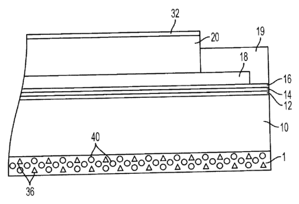
polyurethanes, poly(cyclo olefins), and epoxies, and random or alternating
copolymers thereof. In embodiments, the charge transport layer, such as a hole
transport layer, may have a thickness of at least about 10 pm, or no more than
about
40 pm.
[0060] Examples of components or materials optionally incorporated into the
charge transport layers or at least one charge transport layer to, for
example, enable
improved lateral charge migration (LCM) resistance include hindered phenolic
antioxidants such as tetrakis methylene(3,5-cli-tert-butyl-4-hydroxy
hydrocinnamate)
methane (IRGANOX 1010, available from Ciba Specialty Chemical), butylated
hydroxytoluene (BHT), and other hindered phenolic antioxidants including
SUMILIZERTm BHT-R, MDP-S, BBM-S, WX-R, NW, BP-76, BP-101, GA-80, GM and
GS (available from Sumitomo Chemical Co., Ltd.), IRGANOX 1035, 1076, 1098,
1135, 1141, 1222, 1330, 1425WL, 1520L, 245, 259, 3114, 3790, 5057 and 565
(available from Ciba Specialties Chemicals), and ADEKA STABTm A0-20, A0-30,
A0-40, A0-50, A0-60, A0-70, A0-80 and A0-330 (available from Asahi Denka Co.,
Ltd.); hindered amine antioxidants such as SANOLTM LS-2626, LS-765, LS-770 and
LS-744 (available from SANKYO CO., Ltd.), TINUVIN 144 and 622LD (available
from Ciba Specialties Chemicals), MARKTM LA57, LA67, LA62, LA68 and LA63
(available from Asahi Denka Co., Ltd.), and SUMILIZER TPS (available from
Sumitomo Chemical Co., Ltd.); thioether antioxidants such as SUMILIZER TP-D
(available from Sumitomo Chemical Co., Ltd); phosphite antioxidants such as
MARKTM 2112, PEP-8, PEP-24G, PEP-36, 329K and HP-10 (available from Asahi
Denka Co., Ltd.); other molecules such as bis(4-diethylamino-2-methylphenyl)
phenylmethane (BDETPM), bis-[2-methyl-4-(N-2-hydroxyethyl-N-ethyl-
aminopheny1)]-phenylmethane (DHTPM), and the like. The weight percent of the
antioxidant in at least one of the charge transport layer is from about 0 to
about 20,
from about 1 to about 10, or from about 3 to about 8 weight percent.
[0061] The charge transport layer should be an insulator to the extent that
the
electrostatic charge placed on the hole transport layer is not conducted in
the
absence of illumination at a rate sufficient to prevent formation and
retention of an
electrostatic latent image thereon. The charge transport layer is
substantially
nonabsorbing to visible light or radiation in the region of intended use, but
is
19
CA 02701016 2010-04-19
electrically "active" in that it allows the injection of photogenerated holes
from the
photoconductive layer, that is the charge generation layer, and allows these
holes to
be transported through itself to selectively discharge a surface charge on the
surface
of the active layer.
[0062] Any suitable and conventional technique may be utilized to form and
thereafter apply the charge transport layer 20 mixture to the charge
generating layer
18. The charge transport layer 20 may be formed in a single coating step or in
multiple coating steps. Dip coating, ring coating, spray, gravure or any other
drum
coating methods may be used.
[0063] Drying of the deposited coating may be effected by any suitable
conventional technique such as oven drying, infra red radiation drying, air
drying and
the like. The thickness of the charge transport layer after drying is from
about 10 pm
to about 40 pm or from about 12 pm to about 36 pm for optimum photoelectrical
and
mechanical results. In another embodiment the thickness is from about 14 pm to
about 36 pm.
[0064] In addition, in the present embodiments using a belt configuration, the
charge transport layer 20 may comprise of a single pass charge transport layer
or a
dual pass charge transport layer (or dual layer charge transport layer) with
the same
or different transport molecule ratios. In these embodiments, the dual layer
charge
transport layer has a total thickness of from about 10 pm to about 40 pm. In
other
embodiments, each layer of the dual layer charge transport layer may have an
individual thickness of from 2 pm to about 20 pm. Moreover, the charge
transport
layer may be configured such that it is used as a top layer of the
photoreceptor to
inhibit crystallization at the interface of the charge transport layer and the
overcoat
layer. In another embodiment, the charge transport layer may be configured
such
that it is used as a first pass charge transport layer to inhibit
microcrystallization
occurring at the interface between the first pass and second pass layers.
[0065] Since the charge transport layer 20 is applied by solution coating
process, the applied wet film is dried at elevated temperature and then
subsequently
cooled down to room ambient. The resulting photoreceptor web if, at this
point, not
restrained, will spontaneously curl upwardly into a 1 1/2 inch tube due to
greater
dimensional contraction and shrinkage of the Charge transport layer than that
of the
substrate support layer 10.
20
CA 02701016 2010-04-19
[0066] The Overcoat Layer
[0067] Other layers of the imaging member may include, for example, an
optional over coat layer 32. An optional overcoat layer 32, if desired, may be
disposed over the charge transport layer 20 to provide imaging member surface
protection as well as improve resistance to abrasion. Therefore, typical
overcoat
layer is formed from a hard and wear resistance polymeric material. In
embodiments,
the overcoat layer 32 may have a thickness ranging from about 0.1 micrometer
to
about 10 micrometers or from about 1 micrometer to about 10 micrometers, or in
a
specific embodiment, about 3 micrometers. These overcoating layers may include
thermoplastic organic polymers or inorganic polymers that are electrically
insulating
or slightly semi-conductive. For example, overcoat layers may be fabricated
from a
dispersion including a particulate additive in a resin. Suitable particulate
additives for
overcoat layers include metal oxides including aluminum oxide, non-metal
oxides
including silica or low surface energy polytetrafluoroethylene (PTFE), and
combinations thereof. Suitable resins include those described above as
suitable for
photogenerating layers and/or charge transport layers, for example, polyvinyl
acetates, polyvinylbutyrals, polyvinylchlorides, vinylchloride and vinyl
acetate
copolymers, carboxyl-modified vinyl chloride/vinyl acetate copolymers,
hydroxyl-
modified vinyl chloride/vinyl acetate copolymers, carboxyl- and hydroxyl-
modified
vinyl chloride/vinyl acetate copolymers, polyvinyl alcohols, polycarbonates,
polyesters, polyurethanes, polystyrenes, polybutadienes, polysulfones,
polyarylethers, polyarylsulfones, polyethersulfones, polyethylenes,
polypropylenes,
polymethylpentenes, polyphenylene sulfides, polysiloxanes, polyacrylates,
polyvinyl
acetals, polyamides, polyimides, amino resins, phenylene oxide resins,
terephthalic
acid resins, phenoxy resins, epoxy resins, phenolic resins, polystyrene and
acrylonitrile copolymers, poly-N-vinylpyrrolidinones, acrylate copolymers,
alkyd
resins, cellulosic film formers, poly(amideimide), styrene-butadiene
copolymers,
vinylidenechloride-vinylchloride copolymers, vinylacetate-vinylidenechloride
copolymers, styrene-alkyd resins, polyvinylcarbazoles, and combinations
thereof.
Overcoating layers may be continuous and have a thickness of at least about
0.5
pm, or no more than 10 pm, and in further embodiments have a thickness of at
least
about 2 pm, or no more than 6 pm.
21
CA 02701016 2010-04-19
[0068] The Anti-Curl Back Coatinq Laver
[0069] Since the photoreceptor web exhibits spontaneous upward curling after
completion of charge transport layer coating process, an anti-curl back
coating is
required to be applied to the back side of the substrate to counteract the
curl and
render flatness. The anti-curl back coating 1 may comprise organic polymers or
inorganic polymers that are electrically insulating or slightly semi-
conductive. The
anti-curl back coating provides flatness and/or abrasion resistance.
[0070] Anti-curl back coating 1 may be formed at the back side of the
substrate 10, opposite to the imaging layers. The anti-curl back coating may
comprise a film forming resin binder and an adhesion promoter additive. The
resin
binder may be the same resins as the resin binders of the charge transport
layer
discussed above. Examples of film forming resins include polyacrylate,
polystyrene,
bisphenol polycarbonate, poly(4,4'-isopropylidene diphenyl carbonate), 4,4'-
cyclohexylidene diphenyl polycarbonate, and the like. Adhesion promoters used
as
additives include 49,000 resin (Rohm and Haas), Vitel PE-100, Vitel PE-200,
Vitel
PE-307 (Goodyear), and the like. Usually from about 1 to about 15 weight
percent
adhesion promoter is selected for film forming resin addition. The thickness
of the
anti-curl back coating is at least about 3 pm, or no more than about 35 pm, or
about
14 pm.
[0071] The thermal coefficiency of the disclosed ACBC is important and
should match that of the photo-active layers, in order to produce adequate
counteracting result against the upward P/R curling effect and achieve the
flatness of
the photoreceptor devices. In the present embodiments, the ACBC is also
optically
transparent in the light wavelength of erasing light. Furthermore, the ACBC of
the
present embodiments has the desired static-electron dissipation capability
that is
preferred, and high wear resistance as well in order to have a long
application life.
[0072] As previously discussed, anti-curl back coating (ACBC) layers
incorporating a thermoplastic material pre-compounded to provide sufficient
conductivity to give the anti-curl back coating layer adequate static charge
dissipation capability which provides satisfactory electrical conductivity,
optical
transmission and adequate anti-curling capability. In particular, the present
embodiments provide an anti-curl back coating formulation which demonstrates
both
dispersion stability and improved electrical conductivity by replacing the
high
molecular weight polycarbonate, that is often used in the conventional
(typical) anti-
22
CA 02701016 2010-04-19
curl back coating design, with a pre-compounded anti-static copolymer
comprising of
polyester, polycarbonate, and polyethylene glycol units in the molecular
chain. The
formed anti-curl back coating layer, in embodiments, exhibits good electrical
conductivity and optical transparency as well.
[0073] Fig. 1 shows an imaging member having a belt configuration according
to the embodiments. In the present embodiments, the anti-curl back coating 1
comprises a solid solution of an adhesion promoter 36 and a thermoplastic
material
40. In particular embodiments, the thermoplastic material 40 comprises an anti-
static copolymer having polyester, polycarbonate, and polyethylene glycol
units in
the molecular chain. In Fig. 1, the thermoplastic copolymer 40 and adhesion
promoter 36 are illustrated and presented as separated entities, similar to
that of
particle dispersions in the material matrix of anti-curl back coating 1.
However, this
representation is solely for convenience in discussing the disclosure, and in
reality,
both the thermoplastic copolymer and the adhesion promoter do in fact form a
homogeneous solid solution without phase separation. In embodiments, the
adhesion promoter 36 is present in an amount of from about 1% to about 15%, or
from about 5% to about 10%, by weight of the total weight of the resulting
anti-curl
back coating layer 1. In other embodiments, the thermoplastic material 40 is
present
in an amount of from about 85% to about 99%, or from about 90% to about 95% by
weight of the anti-curl back coating layer 1. In yet further embodiments, the
weight/weight ratio of the adhesion promoter 36 to the thermoplastic material
or
copolymer of polycarbonate 40 present in the anti-curl back coating layer is
from
about 1/99 to about 15/85. In addition, between about 0.5% and about 10% by
weight polytetrafluoroethylene (PTFE) or silica dispersion, based on the total
weight
of the layer, may also be incorporated into the present embodiments to provide
enhanced wear resistance to the anti-curl back coating layer of this
disclosure.
[0074] The present embodiments provide a conductively and optically suitable
anti-curl back coating layer having suitable optical transmission as well as
electrical
conductivity. For example, the embodiments provide an anti-curl back coating
layer
that exhibits an optical transparency of greater than 70 percent transmission
based
on total radiant energy transmitted through the coating layer. The present
embodiments provide the desired higher transparency. The anti-curl back
coating
layer also exhibits, in embodiments, a surface resistivity of from about 1.0 X
104 to
about 1.0 X 10¹⁴ ohm/sq, or from about 1.0 X 10⁶ to about 1.0 X 10¹² ohm/sq.
The
23
CA 02701016 2010-04-19
present embodiments exhibit excellent adhesion to the substrate, good anti-
curling
capability, and adequate optical clarity to allow photoreceptor belt back
erase.
[0075] In alternative embodiments, shown in Fig. 2, the anti-curl back coating
of this disclosure may comprise of dual layers¨an inner layer 2 and an outer
layer 3.
For the dual layers of anti-curl back coating design, the inner (or bottom)
layer is a
standard/conventional polycarbonate anti-curl back coating applied directly
onto the
substrate support 10 while the outer (or top) thermoplastic (anti-static)
copolymer
layer is then solution coated over and fusion bonded to the inner layer
without the
need of adhesion promoter. The inner layer 2 may optionally comprise an
adhesion
promoter. However, the outer layer 3 comprises the anti-static thermoplastic
copolymer 40 may also include an adhesion promoter. As stated above, for Fig.
1,
the thermoplastic copolymer 40 and adhesion promoter 36 are illustrated and
presented as separated entities, similar to that of particle dispersions in
the material
matrix of anti-curl back coating for ease of reference. In another alternative
embodiments, the inner layer 2 comprises the anti-static thermoplastic
copolymer 40
and an adhesion promoter while the outer layer 3 is formulated to comprise
carbon
nanotube (CNT) dispersion in the thermoplastic copolymer 40.
[0076] For dual layered anti-curl back coating design, the thickness of the
inner layer may be thinner, thicker than, or equal to that of the anti-static
outer layer.
Nonetheless, the inner layer is preferred to be less than the outer layer.
[0077] For additional embodiments, shown in Fig. 3, the disclosed anti-curl
back coating may be prepared to comprise of triple layers comprising of an
inner
layer 2, an intermediate layer 3, and an outer layer 4. In this triple-layered
anti-curl
back coating, the inner layer is a thin conventional polycarbonate layer, the
intermediate layer is an anti-static thermoplastic copolymer 40 layer, and the
outer
layer 4 is a highly electrically conductive layer containing carbon nanotube
(CNT)
particles dispersion 42 in anti-static thermoplastic matrix. The inner layer
may
optionally comprise the adhesion promoter 36 while the intermediate layer and
outer
layer are capable of fusion bonding that requires no adhesion promoter
addition. In
another additional embodiments, the intermediate layer 3 comprises the anti-
static
thermoplastic copolymer 40 layer, and the outer layer 4 is a highly
electrically
conductive layer containing carbon nanotube (CNT) particles dispersion 42 in a
polycarbonate matrix.
24
CA 02701016 2010-04-19
[0078] In extended embodiments of the disclosed triple-layered anti-curl back
coating having a thin conventional polycarbonate inner layer 2, the
intermediate layer
3 is a conductive carbon nanotube dispersed layer of anti-static thermoplastic
copolymer 40, and the outer layer 4 comprises the anti-static thermoplastic
copolymer 40.
[0079] In further extended embodiments of this disclosed triple-layered anti-
curl back coating design having a thin conventional polycarbonate inner layer,
the
intermediate layer is formulated to comprise carbon nanotube dispersed in
polycarbonate material matrix while the outer is the anti-static copolymer
layer.
[0080] The total thickness of the triple-layered anti-curl back coating
depends
on the degree of photoreceptor upward curling after completion of charge
transport
layer, so it has to have a thickness adequately sufficient to
counteract/balance the
curl and provides flatness. The thickness of the inner layer would be about
40% of
that of the thickness of intermediate and outer layers. Although the relative
thickness
between the intermediate layer and the outer layers may be in any suitable
ratio,
nonetheless it is preferred that both these layers have about equal in
thickness.
[0081] In the present disclosure of the above embodiments containing
conductive particle dispersed anti-curl back coating, dispersions of multi-
wall carbon
nanotubes, double-walled carbon nanotubes or single-walled carbon nanotube or
a
mixture thereof, can, however, be used at doping levels so that both the
electrical
conductivity and optical transmission objectives of the formulated anti-curl
back
coating are met. The dispersion level of carbon nanotube particles to activate
suitable is layer conductivity is from about 0.01% to about 20%, and
preferably
between about 0.05% and about 10% by weight based on the total weight of the
anti-
curl back coating.
[0082] Carbon nanotubes, with their unique shapes and characteristics, are
being considered for various applications. A carbon nanotube has a tubular
shape of
one-dimensional nature which can be grown through a nano metal particle
catalyst.
More specifically, carbon nanotubes can be synthesized by arc discharge or
laser
ablation of graphite. In addition, carbon nanotubes can be grown by a chemical
vapor deposition (CVD) technique. With the CVD technique, there are also
variations including plasma enhanced and so forth.
[0083] Carbon nanotubes can also be formed with a frame synthesis
technique similar to that used to form fumed silica. In this technique, carbon
atoms
25
CA 02701016 2010-04-19
are first nucleated on the surface of the nano metal particles. Once
supersaturation
of carbon is reached, a tube of carbon will grow.
[0084] Regardless of the form of synthesis, and generally speaking, the
diameter of the tube will be comparable to the size of the nanoparticle.
Depending
on the method of synthesis, reaction condition, the metal nanoparticles,
temperature
and many other parameters, the carbon nanotube can have just one wall,
characterized as a single-walled carbon nanotube, it can have two walls,
characterized as a double-walled carbon nanotube, or can be a multi-walled
carbon
nanotube. The purity, chirality, length, defect rate, etc. can vary. Very
often, after
the carbon nanotube synthesis, there can occur a mixture of tubes with a
distribution
of all of the above, some long, some short. Some of the carbon nanotubes will
be
metallic and some will be semiconducting. Single wall carbon nanotubes can be
about 1 nm in diameter whereas multi-wall carbon nanotubes can measure several
tens nm in diameter, and both are far thinner than their predecessors, which
are
called carbon fibers. It will be appreciated that differences between carbon
nanotube
and carbon nano fiber is decreasing with the rapid advances in the field. For
purposes of the present embodiments, it will be appreciated that the carbon
nanotube is hollow, consisting of a "wrapped" graphene sheet. In contrast,
while the
carbon nano fiber is small, and can even be made in dimension comparable to
some
large carbon nanotubes, it is a solid structure rather than hollow.
[0085] Carbon nanotubes in the present embodiments can include ones that
are not exactly shaped like a tube, such as: a carbon nanohorn (a horn-shaped
carbon nanotube whose diameter continuously increases from one end toward the
other end) which is a variant of a single-wall carbon nanotube; a carbon
nanocoil (a
coil-shaped carbon nanotube forming a spiral when viewed in entirety); a
carbon
nanobead (a spherical bead made of amorphous carbon or the like with its
center
pierced by a tube); a cup-stacked nanotube; and a carbon nanotube with its
outer
periphery covered with a carbon nanohorn or amorphous carbon.
[0086] Furthermore, carbon nanotubes in the present embodiments can
include ones that contain some substances inside, such as: a metal-containing
nanotube which is a carbon nanotube containing metal or the like; and a peapod
nanotube which is a carbon nanotube containing a fullerene or a metal-
containing
fullerene.
26
CA 02701016 2010-04-19
[0087] As described above, in the present embodiments, it is possible to
employ carbon nanotubes of any form, including common carbon nanotubes,
variants of the common carbon nanotubes, and carbon nanotubes with various
modifications, without a problem in terms of reactivity. Therefore, the
concept of
"carbon nanotube" in the present embodiments encompasses all of the above.
[0088] One of the characteristics of carbon nanotubes resides in that the
aspect ratio of length to diameter is very large since the length of carbon
nanotubes
is on the order of micrometers, and can vary from about 200 nm to as long as 2
mm.
Depending upon the chirality, carbon nanotubes can be metallic and
semiconducting.
[0089] Carbon nanotubes excel not only in electrical characteristics but also
in
mechanical characteristics. That is, the carbon nanotubes are distinctively
tough, as
attested by their Young's moduli exceeding 1 TPa, which belies their extreme
lightness resulting from being formed solely of carbon atoms. In addition, the
carbon
nanotubes have high elasticity and resiliency resulting from their cage
structure.
Having such various and excellent characteristics, carbon nanotubes are very
appealing as industrial materials.
[0090] Applied research that exploits the excellent characteristics of carbon
nanotubes has been extensive. To give a few examples, a carbon nanotube is
added as a resin reinforcer or as a conductive composite material while
another
research uses a carbon nanotube as a probe of a scanning probe microscope.
Carbon nanotubes have also been used as minute electron sources, field
emission
electronic devices, and flat displays.
[0091] As described above, carbon nanotubes can find use in various
applications. In particular, the applications of the carbon nanotubes to
electronic
materials and electronic devices have been attracting attention. In an
electrophotographic imaging process, an electric field can be created by
applying a
bias voltage to the electrophotographic imaging components, comprising of
resistive
coating or layers. Further, the coatings and material layers are subjected to
a bias
voltage such that an electric field can be created in the coatings and
material layers
when the bias voltage is on and be sufficiently electrically relaxable when
the bias
voltage is off so that electrostatic charges are not accumulated after an
electrophotographic imaging process. The fields created are used to manipulate
unfused toner image along the toner path, for example from photoreceptor to an
27
CA 02701016 2010-04-19
intermediate transfer belt and from the intermediate transfer belt to paper,
before
fusing to form the fixed images. These electrically resistive coatings and
material
layers are typically required to exhibit resistivity in a range of about 1x10⁷
to about
1x10¹² ohm-cm and should possess mechanical and/or surface properties suitable
for a particular application or use on a particular component.
[0092] It has been difficult to consistently achieve this desired range of
resistivity
with known coating materials. Two approaches have been used in the past,
including ionic filler and particle filler; however, neither approach can
consistently
meet complex design requirements without some trade off. For example, coatings
with ionic filler have better dielectric strength (high breakdown voltage),
but the
conductivity is very sensitive to humidity and/or temperature. In contrast,
the
conductivity of particle filler systems are usually less sensitive to
environmental
changes, but the breakdown voltage tends to below.
[0093] More recently, carbon nanotubes have been used in polyimide and
other polymeric systems to produce composites with resistivity in a range
suitable for
electrophotographic imaging devices. Since carbon nanotube is conductive with
very high aspect ratio, the desirable surface conductivity, about 107 to about
1012
ohm/ square (0/sq), can be achieved with very low filler loading. Thus, there
is
presented a significant advantage as the carbon nanotube will not change the
property of the polymer binder at this loading level, and consequently, opens
up
design space for the selection of polymer binder for a given application.
[0094] Accordingly, dispersion of carbon nanotubes is viable approach to be
adopted for flexible electrophotographic imaging member belt applications,
particularly in the coatings and materials of certain components such as, for
example, the photoreceptor anti curl back coating (ACBC). Thus, the present
embodiments provide an alternative use of carbon nanotubes in a dispersion
that
has provided higher conductivity than those presently available materials
disclosed
in prior arts while also being able to maintain a much more stable coating
solution
and pot life. The resulting anti-curl back coating formed from such dispersion
also
have been shown to be optically suitable, for example, achieve relatively high
transparency.
[0095] In further embodiments, 1% to 10%wt of silica or
polytetrafluoroethylene (PTFE) dispersion may also respectively be included
into the
material matrix of the anti-static single layer, the outer layer of a dual-
layer, or the
28
CA 02701016 2010-04-19
outer layer of a triple-layer design to enhance the anti-curl back coating
abrasion/wear resistance of the present disclosure.
[0096] Various exemplary embodiments encompassed herein include a
method of imaging which includes generating an electrostatic latent image on
an
imaging member, developing a latent image, and transferring the developed
electrostatic image to a suitable substrate.
[0097] While the description above refers to particular embodiments, it will
be
understood that many modifications may be made without departing from the
spirit
thereof. The accompanying claims are intended to cover such modifications as
would fall within the true scope and spirit of embodiments herein.
[0098] The presently disclosed embodiments are, therefore, to be considered
in all respects as illustrative and not restrictive, the scope of embodiments
being
indicated by the appended claims rather than the foregoing description. All
changes
that come within the meaning of and range of equivalency of the claims are
intended
to be embraced therein.
[0099]
EXAMPLES
[00100] The example set forth herein below and is illustrative of different
compositions and conditions that can be used in practicing the present
embodiments. All proportions are by weight unless otherwise indicated. It will
be
apparent, however, that the embodiments can be practiced with many types of
compositions and can have many different uses in accordance with the
disclosure
above and as pointed out hereinafter.
[00101] Control Example
[00102] Anti-curl Back Coating Preparation
[00103] A standard anti-curl back coating solution was prepared by dissolving
proper amount of MAKROLON and PE200 adhesive promoter in methylene chloride
to give a coating solution containing 10% wt solid. The resulting solution was
then
applied over a 3 1/2 mil thick poly(ethylene naphthalate) (PEN) substrate
using a 4 1/2
mil gap bar by following the standard hand coating procedures. After drying
the
applied wet coating at 120 C for 1 minute in the air circulating over, a 17
pm dried
ACBC thickness was obtained. The resulting standard anti-curl back coating
layer,
comprising 92% wt Makrolon and 8% wt PE200, did exhibit upwardly curling to
29
CA 02701016 2010-04-19-
provide photoreceptor curl balancing effect. The standard anti-curl back
coating
layer that resulted was to be used as control.
[00104] Disclosure Example 1
[00105] Anti-curl Back Coating Preparation
[00106] The disclosure anti-curl back coating solution was then prepared by
following the same procedures described in the Control Example above, except
that
the polymer used was a thermoplastic material being a pre-compounded polymer
having static-charge dissipation capability needed for total replacement of
MAKROLON. The resulting disclosure anti-curl back coating (containing 8% wt
PE200 adhesion promoter) thus prepared had a 17 pm in dried thickness and been
seen to give equivalent upward curling like that of the standard control anti-
curl back
coating prepared in Control Example.
[00107] The adhesion promoter polyester PE-200 was purchased from Bostik,
Inc. (Wauwatosa, Wisconsin). Anti-static copolymer STAT-LOY 63000 CTC,
comprising of polyester, polycarbonate, and polyethylene glycol units in the
molecular chain, was purchased from Saudi Basic Industries Corporation (SABIC)
(Riyadh, Saudi Arabia); it was a glassy thermoplastic material. Nuclear
magnetic
resonance (NMR) analysis of this compounded polymer showed that it is a
mixture of
about 62 parts of polyester (formed by trans-1,4-cyclohexanedicarboxylic acid
and
trans/cis mixture of 1,4-cyclohexanedimethanol), 33 parts of Bisphenol A
polycarbonate (PCA), and at least 6 parts of polyethylene glycol (PEG).
[00108] Disclosure Example 2
[00109] Dual-Layered Anti-curl Back Coating Preparation
[00110] The disclosure anti-curl back coating was prepared to have a dual
layers comprising of an inner layer and an outer layer. The inner layer,
coated
directly onto the PEN substrate, was a conventional layer prepared in the same
procedures and material compositions according to the description of Control
Example to give a 7 microns dried thickness. The outer layer was then solution
applied over the inner layer in the same manner and material make-up as those
described in Disclosure Example 1, except that PE-200 adhesion promoter was
omitted; after drying at elevated temperature, the outer anti-static layer
gave a 10 pm
dried thickness and was fusion bonded to the inner layer. The resulting dual
anti-curl
back coating layers had a total thickness of about 17 pm and showed the same
30
CA 02701016 2010-04-19
degree of upward curling as that seen in the anti-curl back coating of control
Example.
[00111] Disclosure Example 3
[00112] Triple-layered Anti-curl Back Coating Preparation
[00113] In this conceptually constructed example, the anti-curl back coating
of
this disclosure may be prepared to comprise triple layers, comprising of an
inner
layer, an intermediate layer, and an outer layer. In this triple-layered anti-
curl back
coating design, it would have a thin conventional polycarbonate inner layer,
an anti-
static thermoplastic intermediate layer, and a highly electrically conductive
outer
layer containing carbon nanotube particles dispersion in anti-static
thermoplastic
matrix. In this triple layered anti-curl back coating design, addition of an
adhesion
promoter may optionally be omitted from both inner layer and outer layer
formulations, because they will be fusion bonded to each other and to the
inner
polycarbonate layer as well by solution application. In embodiments, the
carbon
nanotube may be selected from the group consisting of single-walled carbon
nanotube, double-walled carbon nanotube, multi-walled carbon nanotube, or
mixtures thereof.
[00114] The total thickness of the triple-layered anti-curl back coating
depends
on the degree of photoreceptor upward curling after completion of charge
transport
layer, so it has to have a thickness adequately sufficient to
counteract/balance the
curl and provides flatness. The thickness of the inner layer would be about
40% of
that of the thickness of intermediate and outer layers. Although the relative
thickness
between the intermediate layer and the outer layers may be in any suitable
ratio,
nonetheless it is preferred that both these layers have about equal in
thickness.
[00115] The preparation of the inner layer and the intermediate layer were
following the same procedures and using the same materials as those detailed
in the
above Disclosure Example 2.
[00116] However, the carbon nanotube dispersion-containing outer layer (with
or optionally without adhesion promoter) is prepared by following either one
of the
two procedures detailed below:
[00117] Procedure l: Single-walled nanotubes dispersed outer layer
[00118] A methylene chloride dispersion of a soluble single walled carbon
nanotube dispersion with the high molecular weight polycarbonate was purchased
from Zyvex. This dispersion had about 0.375 % by weight of the single walled
31
CA 02701016 2010-04-19
= w
carbon nanotube and about 9.0 % polycarbonate. Adhesion promoter polyester PE-
200 was purchased from Bostik, Inc. (Wauwatosa, Wisconsin). Anti-static
copolymer
STAT-LOY 63000 CTC, comprising of polyester, polycarbonate, and polyethylene
glycol units in the molecular chain, was purchased from Saudi Basic Industries
Corporation (SABIC) (Riyadh, Saudi Arabia). Bisphenol A polycarbonate (PC) or
4,4'-isopropylidenediphenol (FPC-0170, lot #5BF2262) was purchased from
Mitsuibishi Chemical Corporation (Tokyo, Japan).
[00119] Table 1 provides the formulations for the experimental anti-curl
back
coating layer dispersions using the single walled carbon nanotube, and where
"g"
represents grams.
Table 1. Formulation for Conductive ACBC
Sample 0.375% Single- PE- Polycabonate Binder PTFE Methylene
ID walled Carbon 200 (9) (9) (g) Chloride
Nanotube (9) (9)
dispersion (g)
1 3.0 0.13 1.49 STAT- 0 16.40
LOY: 0
2 19.5 1.23 0 STAT- 1.23 82.65
LOY:
7.48
[00120] The materials in each sample were mixed by a roll-mill for 18
hours.
The resulted dispersions were coated on a MYLAR substrate by a 4.0-mil draw
bar,
and dried at 120 C for 1 minute. After being dried, both samples above
contained
0.625 % single walled carbon nanotube.
[00121] Electrical Test
[00122] Surface resistivity measurements were performed on the prepared
anti-
curl back coating layers by a HIRESTA-UP MCP-HT450 high resistivity meter,
available from Mitsubishi Chemical Corporation (Tokyo, Japan). Table 2
illustrates
the results of the surface resistivity measurements (unit of the resistivity
is: Q/sq),
and where "V" represents volts.
Table 2. Surface Resistivity Measurement Results
Voltage 10 V 100 V 250 V 500 V 1000 V
Sample 1 1.0 x 10¹² 1.0 x 10¹³ 1.0 x 10¹³ 1.0 x 10¹⁴ 1.0 x 10¹⁴
Sample 2 8.43 x 10¹⁰ 2.05 x 10¹⁰ 7.96 x 10⁹ 4.38 x 10⁹ 3.70 x 10⁹
32
CA 02701016 2010-04-19
[00123] From these measurement results, with STAT-LOY copolymer as
binder, the anti-curl back coating showed much lower surface resistivity,
compared
with polycarbonate alone as binder. This indicates that lower single walled
carbon
nanotube could be used in conductive ACBC to achieve good surface
conductivity,
which providing a window to fabricate ACBC with high transparency and high
conductivity.
[00124] The coefficient of friction of the coated anti-curl back coating
with
aluminium was also measured. The results are listed in Table 3.
[00125]
Table 3. Coefficient of Friction for Conductive ACBC
Sample Coefficient of Static Friction (Us) Coefficient of Kinetic
Friction (Uk)
ID
1 4.568 4.441
2 5.185 3.844
[00126] With PTFE and STAT-LOY copolymer, the anti-curl back coating had
lower kinetic coefficient of friction, which is highly desirable for a high
performance
anti-curl back coating layer.
[00127] Finally, optical transmission measurements were also taken.
Optical
transmission of the ACBC on poly(ethylene terephthalate) film was measured by
a
Perkin Elmer UV/Vis-NIR spectrometer, Lambda 19. There was no significant OD
difference between these two samples, even though Sample (2) had PTFE and
STAT-LOY copolymer. This result clearly demonstrates that the inventive anti-
curl
back coating can have high surface conductivity and high optical transparency.
[00128] Procedure 11: Multi-walled nanotubes dispersed outer layer
[00129] 1 % soluble multi walled carbon nanotube solution in methylene
chloride was purchased from Zyvex. Adhesion promoter polyester PE-200 was
purchased from Bostik, Inc. (Wauwatosa, Wisconsin). Anti-static copolymer STAT-
LOY 63000 CTC, comprising of polyester, polycarbonate, and polyethylene glycol
units in the molecular chain, was purchased from Saudi Basic Industries
Corporation
(SABIC) (Riyadh, Saudi Arabia). Bisphenol A polycarbonate (PC) or 4,4'-
isopropylidenediphenol (FPC-0170) was purchased from Mitsuibishi Chemical
Corporation (Tokyo, Japan).
33
CA 02701016 2010-04-19
[00130] Table 4 provides the formulations for the experimental anti-
curl back
coating layer dispersions using multi-walled carbon nanotube, and where "g"
represents grams.
Table 4. Formulation for Conductive ACBC
Sample 1% Multi-walled Carbon PE-200
Binder (g) Methylene
ID Nanotube Dispersion (g) _ (g)
Chloride (g)
1 2.7 0.216 STAT-LOY:
24.6
2 8.1 0.216 STAT-LOY:
2.457 19.2
2.403
3 2.7 0.216 PC:
2.457 24.6
4 8.1 0.216 PC:
2.403 19.2
[00131] The materials in each sample were mixed by using a roll-mill
for 18
hours. The resulting solutions were each hand coated on a MYLAR substrate by
using a 4.5-mil gap bar, and subsequently dried at 120 C for 1 minute. After
being
dried, Samples (1) and (3) contained 1% multi walled carbon nanotubes, and
Samples (2) and (4) contained 3% multi walled carbon nanotubes.
[00132] After letting the coated samples sit still on the bench for
one week,
Samples (1) and (2) with STAT-LOY as binder for the carbon nanotube showed no
observable precipitation, while Samples (3) and (4) had obvious phase
separation.
This is related to the dispersion stability of the carbon nanotube. Carbon
nanotubes,
having large cohesive energy density owing to their very large surface area as
well
as strong 7-7 interaction, tend to form bundles and cause low dispersibility
in
common organic solvents.
[00133] Electrical Test
[00134] Surface resistivity measurements were performed on the
prepared anti-
curl back coating layers by a HIRESTA-UP MCP-HT450 high resistivity meter,
available from Mitsubishi Chemical Corporation (Tokyo, Japan). Table 5
illustrates
the results of the surface resistivity measurements (unit of the resistivity
is: Disq),
and where "V" represents volts.
Table 5. Surface Resistivity Measurement Results
Voltage , 10 V 100 V 250V
500V 1000 V
34
CA 02701016 2010-04-19
=
Sample 1 9.64 x 10¹¹ 8.14 x 10¹¹ 7.97 x 10¹¹ 7.85 x 10¹¹ 7.76 x 10¹¹
Sample 2 > 1.0 x 10¹⁴ 8.79 X 10 11 8.45 x 10¹¹ 7.82 x 10¹¹ 6.83 x 10¹¹
Sample 3 > 1.0 x 10¹⁴ > 1.0 x 10¹⁴ > 1.0 x 10¹⁴ > 1.0 x 10¹⁴ > 1.0 x 10¹⁴
Sample 4 > 1.0 x 10¹⁴ > 1.0 x 10¹⁴ > 1.0 x 10¹⁴ > 1.0 x 10¹⁴ > 1.0 x 10¹⁴
[00135] From the above measurement results, one can see that with STAT-
LOY copolymer as binder, the re-formulated anti-curl back coating layer showed
much lower surface resistivity as compared to that using polycarbonate as
binder.
There was no significant difference in surface resistivity for samples using
the anti-
static copolymer as binder or different carbon nanotube as filler in the
experimental
range. This result indicates that both single-walled and multi-walled carbon
nanotubes can be used in the formulation of the present inventive conductive
anti-
curl back coating formulation to achieve good stability and surface
conductivity which
therefore provides a practical method for fabricating anti-curl back coating
layers that
have high transparency and high conductivity.
[00136] The outer nanotube dispersed layer prepared according to either
procedures may optionally contain no adhesive promoter PE200, since the
solution
coated outer layer would fusion be fusion bonded to the intermediate anti-
static
thermoplastic layer.
[00137] Disclosure Example 4
[00138] Triple-layered Anti-curl Back Coating Preparation
[00139] In this example, the triple-layered anti-curl back coating of this
disclosure would be prepared in the same manners and of identical material
compositions as those detailed in Disclosure Example 3 above, but with the
exception that the inner anti-static thermoplastic copolymer layer and the
outer
carbon nanotube dispersed layer would be exchanged in position.
[00140] Results
[00141] Comparison of the disclosure conductive anti-curl back coating
layer
prepared to give single layer and dual layers to that of the standard anti-
curl back
coating control prepared according to the three working examples given above
demonstrate that the anti-curl back coating layer of Disclosure Examples 1 and
2
had equivalent anti-curling capability to provide photoreceptor counter-
curling effect,
adhesion bonding strength to the PEN substrate, and approximately the same
optical
transparency. More importantly, the disclosure anti-curl back coating of
either
35
CA 02701016 2011-11-21
formulation was found to give a surface resistivity of about 9 x 10⁹ ohm/sq.
which is
lower than the electrically insulative standard control.
[00142] From the above measurement results, one can see that an anti-curl
back coating formulation that incorporates the thermoplastic material
disclosed
herein provides an anti-curl back coating layer with much lower surface
resistivity as
compared to a standard anti-curl back coating layer without the thermoplastic
material. There was no significant difference in anti-curling capability for
samples
using the thermoplastic material as binder in the experimental range as
compared to
the control sample. This result indicates that the a thermoplastic material,
such as
one comprising an anti-static copolymer, can be used in the formulation of the
present inventive conductive anti-curl back coating formulation to achieve
good anti-
curling performance and surface conductivity which therefore provides a
practical
method for fabricating anti-curl back coating layers that have high
transparency and
high conductivity.
[00143] It will be appreciated that several of the above-disclosed and other
features and functions, or alternatives thereof, may be desirably combined
into many
other different systems or applications. Also that various presently
unforeseen or
unanticipated alternatives, modifications, variations or improvements therein
may be
subsequently made by those skilled in the art which are also intended to be
encompassed by the following claims. Unless specifically recited in a claim,
steps or
components of claims should not be implied or imported from the specification
or any
other claims as to any particular order, number, position, size, shape, angle,
color, or
material.
36