Note: Descriptions are shown in the official language in which they were submitted.
CA 02701180 2010-03-30
WO 2009/079744 PCT/CA2008/001623
NON-VOLATILE SEMICONDUCTOR MEMORY DEVICE WITH POWER
SAVING FEATURE
CROSS-REFERENCE TO RELATED APPLICATION
The present application claims the benefit under 35
U.S.C. 119(e) of United States Provisional Patent
Application Serial No. 61/015,724, filed on December 21,
2007, hereby incorporated by reference herein.
The present application also claims the benefit under 35
U.S.C. 119(e) of United States Provisional Patent
Application Serial No. 61/048,737, filed on April 29,
2008, hereby incorporated by reference herein.
BACKGROUND
Non-volatile memory is used for various purposes mainly
related to persistent data storage with possibility of
modification. Practical applications of non-volatile re-
writable memory include storage of digital pictures,
computer files, digitally recorded music and so on.
Thus, it is common to find non-volatile re-writable
memory devices in everyday electronics such as computers,
digital cameras, MP3 players, answering machines, cell
phones, etc.
There are many ways in which data can be physically
stored by a non-volatile memory device that also allows
re-writing. One example is by using a magnetic disk as
can be found in many computer hard drives. Another
example is by way of an optical disk such as a CD-R/W.
CA 02701180 2010-03-30
WO 2009/079744 PCT/CA2008/001623
Yet another example is by means of a solid state memory
circuit such as an electrically erasable and programmable
read-only memory (EEPROM), a specific example of which is
a flash memory device. A flash memory device utilizes a
high voltage to erase a large block of non-volatile
memory cells in one operation, allowing these cells to
then be reprogrammed with new data. By virtue of their
robustness, convenience and low cost, flash memory
devices have gained immense popularity in the marketplace
for non-volatile memory and are expected to become even
more dominant as the demand for non-volatile memory
continues to grow unabated.
In the years since flash memory was first introduced,
technological refinements have been made in order to
allow flash memory devices to be operated at increasingly
higher speeds. This has further expanded the breadth of
consumer applications such as, for example, certain video
and photo related applications, in which flash memory
devices can be used. However, faster operation of a
flash memory device can also lead to specific problems
when attempting to create a large high-speed memory store
from multiple devices. In particular, the electrical
power consumption of flash memory, which increases with
operating frequency, can significantly limit the overall
capacity of the memory store being created.
Against this background, there is clearly a need for a
non-volatile semiconductor memory device with reduced
power consumption.
SUMMARY
2
CA 02701180 2010-03-30
WO 2009/079744 PCT/CA2008/001623
A first aspect of the present invention seeks to provide
a non-volatile semiconductor memory device, which
comprises (i) an interface having an input port for
receiving an input clock signal and a set of data lines
for receiving commands, including an erase command, the
commands issued by a controller; (ii) a module having
circuit components in a feedback loop configuration, the
module being driven by a reference clock signal; (iii) a
clock control circuit capable of controllably switching
between a first operational state in which the reference
clock signal tracks the input clock signal and a second
operational state in which the reference clock signal is
decoupled from the input clock signal; and (iv) a command
processing unit configured to recognize the commands
issued by the controller and to cause the clock control
circuit to switch from the operational state to the
second operational state in response to recognizing the
erase command. When the reference clock signal tracks
the input clock signal, the module consumes a first
amount of power and wherein when the reference clock
signal is decoupled from the input clock signal, the
module consumes a second amount of power that is less
than the first amount of power.
A second aspect of the present invention seeks to provide
a non-volatile semiconductor memory device, which
comprises first means for providing an input clock
signal; second means having circuit components in a
feedback loop configuration and being driven by a
reference clock signal; third means for controllably
switching between a first operational state in which the
reference clock signal tracks the input clock signal and
a second operational state in which the reference clock
signal is decoupled from the input clock signal; and
3
CA 02701180 2010-03-30
WO 2009/079744 PCT/CA2008/001623
fourth means for recognizing commands issued by a
controller, including an erase command, and varying the
operational state of the third means in response to
recognizing the erase command. When the reference clock
signal tracks the input clock signal, the second means
consumes a first amount of power and wherein when the
reference clock signal is decoupled from the input clock
signal, the second means consumes a second amount of
power that is less than the first amount of power.
A third aspect of the present invention seeks to provide
a method implemented by a non-volatile semiconductor
memory device. The method comprises providing an input
clock signal; providing a module with circuit components
in a feedback loop configuration and being driven by a
reference clock signal; producing the reference clock
signal such that it follows the input clock signal in a
first operational state of the device and such that it is
decoupled from the input clock signal in a second
operational state of the device, wherein when the
reference clock signal follows the input clock signal,
the module consumes a first amount of power and wherein
when the reference clock signal is decoupled from the
input clock signal, the module consumes a second amount
of power that is less than the first amount of power ;
and causing the device to switch from the first
operational state to the second operational state in
response to recognizing an erase command received from a
controller.
A fourth aspect of the present invention seeks to provide
a system, which comprises a controller configured to
issue a master clock signal and to issue commands
including an erase command; and a non-volatile
4
CA 02701180 2010-03-30
WO 2009/079744 PCT/CA2008/001623
semiconductor memory device. The non-volatile
semiconductor memory device comprises (i) an interface
with an input port for receiving an input clock signal
related to the master clock signal and a set of data
lines for receiving the commands issued by the
controller; (ii) a module having circuit components in a
feedback loop configuration, the module being driven by a
reference clock signal; (iii) a clock control circuit
capable of controllably switching between a first
operational state in which the reference clock signal
tracks the input clock signal and a second operational
state in which the reference clock signal is decoupled
from the input clock signal; and (iv) a command
processing unit configured to recognize the commands
issued by the controller and to cause the clock control
circuit to switch from the first operational state to the
second operational state in response to recognizing the
erase command. When the reference clock signal tracks
the input clock signal, the module consumes a first
amount of power and wherein when the reference clock
signal is decoupled from the input clock signal, the
module consumes a second amount of power that is less
than the first amount of power.
A fifth aspect of the present invention seeks to provide
a computer-readable storage medium comprising computer-
readable instructions which, when processed, are used to
provide a non-volatile semiconductor memory device with
functionality for: producing a reference clock signal
such that it follows an input clock signal in a first
operational state of the device and such that it is
decoupled from the input clock signal in a second
operational state of the device, wherein when the
reference clock signal follows the input clock signal, a
5
CA 02701180 2010-03-30
WO 2009/079744 PCT/CA2008/001623
first amount of power is consumed by a module with
circuit components in a feedback loop configuration that
is driven by the reference clock signal, and wherein when
the reference clock signal is decoupled from the input
clock signal, the module consumes a second amount of
power that is less than the first amount of power; and
causing the device to switch from the first operational
state to the second operational state in response to
recognizing an erase command received from a controller.
Thus, an improved non-volatile semiconductor memory
device has been provided.
BRIEF DESCRIPTION OF THE DRAWINGS
Fig. 1 is a block diagram of a memory system comprising a
controller and a non-volatile memory device, in
accordance with a non-limiting example embodiment.
Fig. 2 is a block diagram of the non-volatile memory
device in Fig. 1 which includes a clock synchronization
unit, in accordance with a non-limiting example
embodiment.
Fig. 3A is a block diagram of the clock synchronization
unit in Fig. 2, in accordance with a non-limiting example
embodiment.
Fig. 3B is a block diagram of the clock synchronization
unit in Fig. 2, in accordance with an alternative example
embodiment.
6
CA 02701180 2010-03-30
WO 2009/079744 PCT/CA2008/001623
Fig. 4A is a timing diagram that shows signal transitions
of various signals associated with the clock
synchronization unit of Fig. 3A.
Fig. 4B is a timing diagram that shows signal transitions
of various signals associated with the clock
synchronization unit of Fig. 3B.
DETAILED DESCRIPTION
Reference is made to Fig. 1, which illustrates a memory
system 80 in accordance with an example embodiment. The
memory system 80 comprises a controller 90
communicatively coupled to a non-volatile memory device
100. The controller 90 may also be communicatively
coupled to other memory devices 100A.
The controller 90 comprises a set of ports 92A..92H, which
are respectively connected to a set of ports 93A...93H of
the non-volatile memory device 100. The controller 90
and the non-volatile memory device 100 exchange device-
external electrical signals 94A..94H via their respective
sets of ports, 92A..92H and 93A..93H. The ports 93A...93H of
the non-volatile memory device 100 and the device-
external signals 94A..94H will be described in greater
detail subsequently herein.
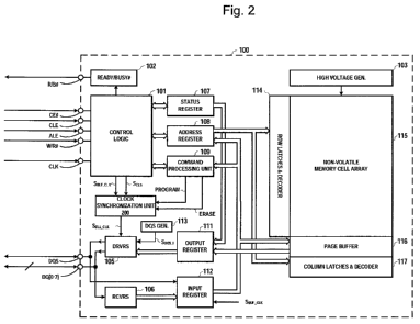
Fig. 2 is a block diagram of the non-volatile memory
device 100 in accordance with an example embodiment.
Within the non-volatile memory device 100, a non-volatile
memory cell array 115 includes a plurality of non-
volatile memory cells arranged in rows and columns. Each
non-volatile memory cell includes a floating-gate field-
7
CA 02701180 2010-03-30
WO 2009/079744 PCT/CA2008/001623
effect transistor capable of holding a charge for the
non-volatile storage of data. The non-volatile memory
cells in the non-volatile memory cell array 115 can be
electrically programmed by charging the floating gate.
The rows of the non-volatile memory cell array 115 can be
arranged in blocks of pages. By way of non-limiting
example, the rows of the non-volatile memory cell array
115 can be organized into 2048 blocks, with 64 pages per
block.
The non-volatile memory device 100 comprises an interface
that includes the aforementioned set of ports 93A...93H.
Among these, ports 93B, 93C, 93D, 93E, 93F (also labeled
CE#, CLE, ALE, W/R#, CLK, respectively) carry device-
external signals from the controller 90 to the non-
volatile memory device 100. Ports 93A (also labeled
R/B#) carries device-external signals from the non-
volatile memory device 100 to the controller 90.
Finally, ports 93G and 93H (also labeled DQS and DQ[0:7],
respectively) are capable of carrying device-external
signals in either direction depending on an operating
mode of the non-volatile memory device 100. More
specifically, the ports of the non-volatile memory device
100 include, without limitation:
= a chip enable port (93B, also labeled CE#):
The chip enable port CE# is an input port that allows
the non-volatile memory device 100 to know whether or
not it has been activated by the controller 90. In the
present non-limiting embodiment, when the device-
external signal at the chip enable port CE# is de-
asserted (LOW), this means that the non-volatile memory
8
CA 02701180 2010-03-30
WO 2009/079744 PCT/CA2008/001623
device 100 has been selected, whereas when the device-
external signal at the chip enable port CE# is asserted
(HIGH), this means that the non-volatile memory device
100 has been de-selected.
= an input clock port (93F, also labeled CLK):
The input clock port CLK is an input port that carries
a clock signal (a system clock) used to synchronize
operation of the non-volatile memory device 100. Thus,
it should be understood that by virtue of being
synchronized to the system clock, the non-volatile
memory device 100 differs from asynchronous or
plesiochronous memory devices.
= a plurality of data lines (93H, also labeled DQ[0:7]):
The data lines DQ[0:7] carry addresses, commands and
write data from the controller 90, as well as carry
read data to the controller 90. While in the
illustrated embodiment there are eight (8) data lines,
this should not be considered a limitation. For
example, in other embodiments, a different number of
data lines may be provided, such as sixteen (16).
Still other possibilities exist.
= a command latch enable port (93C, also labeled CLE) and
an address latch enable port (93D, also labeled ALE):
The command latch enable port CLE and the address latch
enable port ALE are input ports that carry device-
external signals which parallel the device-external
signals on the data lines DQ[0:7] and delineate the
start and end of addresses, commands and/or write data.
9
CA 02701180 2010-03-30
WO 2009/079744 PCT/CA2008/001623
= a data strobe port (93G, also labeled DQS):
The data strobe port DQS carries a device-external
signal that indicates the presence of valid data on the
data lines DQ[0:7]. When data is to be written to the
non-volatile memory device 100 (in a non-limiting
double data rate embodiment), the device-external
signal at the data strobe port DQS is generated by the
controller 90, has the same frequency as the device-
external signal at the input clock port CLK, and is
90 -shifted and center aligned with the device-external
signal on the data lines DQ[0:7]. When data is being
read from the non-volatile memory device 100 (in a non-
limiting double data rate embodiment), the device
external signal at the data strobe port DQS is
generated by the non-volatile memory device 100, has
the same frequency as the device-external signal at the
input clock port CLK, and is edge-aligned with the
device-external signal on the data lines DQ[0:7]. It
should be appreciated that in the absence of valid data
on the data lines DQ[0:7], the device-external signal
at the data strobe port DQS can be made to not
oscillate. As such, there will be periods when the
device-external signal at the data strobe port DQS
oscillates and periods when it does not.
= a write/read port (93E, also labeled W/R#):
The write/read port W/R# is an input port that carries
a device-external signal indicating whether the data
lines DQ[0:7] carry write data from the controller 90
(i.e., when the device-external signal W/R# is HIGH) or
CA 02701180 2010-03-30
WO 2009/079744 PCT/CA2008/001623
carry read data from the memory device 100 (i.e., when
the device-external signal W/R# is LOW).
= a ready/busy port (93A, also labeled R/B#):
The ready/busy port R/B# is an output port that carries
a device-external signal indicating whether the non-
volatile memory device 100 is available to receive a
command for accessing the memory cell array 115 (when
the device-external signal is HIGH) or is busy
processing a command for accessing the memory cell
array 115 (when the device-external signal is LOW).
The controller 90 controls behavior of the non-volatile
memory device 100 by varying the device-external signals
at the various input ports and on the data lines.
Accordingly, the non-volatile memory device 100 comprises
control logic 101 that is configured to recognize when
the input ports and data lines carry certain specific
signals from the controller 90, and to respond in a
deterministic way based upon these signals.
For example, the control logic 101 is configured to
recognize when the device-external signal at the command
latch enable port CLE is HIGH and the device-external
signal at the address latch enable port ALE is LOW. In
this case, the control logic 101 considers that the
information on the data lines DQ[0:7] is command
information. Accordingly, the information on the data
lines DQ[0:7] is received by an input receiver 106,
latched into an input register 112 on the rising edge of
a buffered clock signal SBUFCLK (which is a buffered
version of the device-external signal at the input clock
port CLK and has the same polarity) and provided to a
11
CA 02701180 2010-03-30
WO 2009/079744 PCT/CA2008/001623
command processing unit 109. The command processing unit
109 may include a register into which the information is
loaded and a decoder for decoding the loaded information
into one or more commands. The command processing unit
109 generates control signals, some of which are fed to
the control logic 101 and others of which are fed to the
clock synchronization unit 200, as will be described in
further detail later on.
In some embodiments, the command processing unit 109 is
integrated with the control logic 101, while in other
embodiments, the command processing 109 and the control
logic 101 may be distinct components of the memory device
100. In still other embodiments, portion of the command
processing unit 109 (such as a register) can be distinct
while the remainder of the command processing unit 109
may be integrated with the control logic 101.
There are several examples of commands that can be
processed by the non-volatile memory device 100,
including BLOCK ERASE, PAGE PROGRAM, PAGE READ, STATUS
READ, to name a few non-limiting possibilities. Some of
these commands and their effects are described below by
way of non-limiting example.
A) BLOCK ERASE
When the control logic 101 recognizes a BLOCK ERASE
command (more precisely: an indicative first command
cycle of the BLOCK ERASE command), the control logic
101 is configured to subsequently expect to receive
address information on the data lines DQ[0:7]. Address
information is deemed to be present on the data lines
DQ[0:7] when the device-external signal at the command
12
CA 02701180 2010-03-30
WO 2009/079744 PCT/CA2008/001623
latch enable port CLE is LOW and the device-external
signal at the address latch enable port ALE is HIGH.
Accordingly, the information on the data lines DQ[0:7]
is received by the input receiver 106, latched into the
input register 112 on the rising edge of the
aforementioned buffered clock signal SBUFCLK and
transferred into an address register 108. The address
information, which can span over multiple address
cycles, may include a plurality of bytes specifying the
address of a desired block to be erased. The address
information in its entirety can be loaded into a row
latches and decoder 114.
The control logic 101 is configured to subsequently
expect to receive a second command cycle of the BLOCK
ERASE command on the data lines DQ[0:7]. Accordingly,
when the device-external signal at the command latch
enable port CLE is HIGH and the device-external signal
at the address latch enable port ALE is LOW, the
information on the data lines DQ[0:7] is received by
the input receiver 106, latched into the input register
112 on the rising edge of the buffered clock signal
SBUF_CLK and transferred to the command processing unit
109. The command processing unit 109 recognizes the
second command cycle of the BLOCK ERASE command.
The command processing unit 109 then asserts an ERASE
signal that is used by the clock synchronization unit
200 as will be described herein below. The control
logic 101 causes the device-external signal at the
ready/busy port R/B# to go LOW in order to indicate
that the non-volatile memory device 100 is busy. Also,
The control logic 101 then invokes a high voltage
generator 103 to apply high voltages in order to erase
13
CA 02701180 2010-03-30
WO 2009/079744 PCT/CA2008/001623
the non-volatile memory cells that are within the
desired block. This operation may take an extended
period of time that, for current technology, is within
the range of about 2 milliseconds to about 15
milliseconds, depending on a variety of factors.
After the non-volatile memory cells within desired
block have been erased, the command processing unit 109
de-asserts the ERASE signal. Then, after a time
interval needed by certain components of the clock
synchronization unit 200 to re-acquire synchronization,
the control logic 101 causes the device-external signal
at the ready/busy port R/B# to go HIGH in order to
indicate that the non-volatile memory device 100 is
ready to receive another command.
B) PAGE PROGRAM
When the control logic 101 recognizes a PAGE PROGRAM
command (more precisely: an indicative first command
cycle of the PAGE PROGRAM command), the control logic
101 is configured to subsequently expect to receive
address information on the data lines DQ[0:7]. Address
information is deemed to be present on the data lines
DQ[0:7] when the device-external signal at the command
latch enable port CLE is LOW and the device-external
signal at the address latch enable port ALE is HIGH.
Accordingly, the information on the data lines DQ[0:7]
is received by the input receiver 106, latched into the
input register 112 on the rising edge of the buffered
clock signal SBUFCLK and transferred into the address
register 108. The address information, which can span
over multiple address cycles, may include a plurality
of bytes specifying a desired page to be programmed.
14
CA 02701180 2010-03-30
WO 2009/079744 PCT/CA2008/001623
The address information can be loaded into the row
latches and decoder 114 and/or a column latches and
decoder 117.
The control logic 101 then expects to receive write
data on the data lines DQ[0:7]. This occurs when the
device-external signals at both the command latch
enable port CLE and the address latch enable port ALE,
as well as the device-external signal at the write/read
port W/R#, are all HIGH. Additional use is made of the
device-external signal at the data strobe port DQS. In
this case, the write data being received by the input
receiver 106 is latched into the input register 112 at
both edges of the device-external signal at the data
strobe port DQS and is selected by the column latches
and decoder 117 to be loaded into a page buffer 116.
When the device-external signals at the command latch
enable port CLE and the address latch enable port ALE
are no longer both HIGH, the non-volatile memory device
100 stops latching the write data, and thus the amount
of write data written to the non-volatile memory device
100 is determined by the length of time during which
the device-external signals at both the command latch
enable port CLE and the address latch enable port ALE
had remained HIGH. For example, if the device-external
signals at both the command latch enable port CLE and
the address latch enable port ALE had remained HIGH for
1024 clock cycles, the non-volatile memory device 100
would have received 2048 bytes of write data (for an 8-
bit-wide data bus in a double data rate scenario).
The control logic 101 is configured to subsequently
expect to receive a second command cycle of the PAGE
CA 02701180 2010-03-30
WO 2009/079744 PCT/CA2008/001623
PROGRAM command on the data lines DQ[0:7].
Accordingly, when the device-external signal at the
command latch enable port CLE is HIGH and the device-
external signal at the address latch enable port ALE is
LOW, the information on the data lines DQ[0:7] is
received by the input receiver 106, latched into the
input register 112 on the rising edge of the buffered
clock signal SBUFCLK and transferred into the command
processing unit 109. The command processing unit 109
recognizes the second command cycle of the PAGE PROGRAM
command.
The command processing unit 109 then asserts a PROGRAM
signal that is used by the clock synchronization unit
200 as will be described herein below. In addition,
the control logic 101 causes the device-external signal
at the ready/busy port R/B# to go LOW in order to
indicate that the non-volatile memory device 100 is
busy. The control logic 101 then invokes the high
voltage generator 103 to apply high voltages in order
to transfer the write data in the page buffer 116 to
the desired page in the non-volatile memory cell array
115. This operation may take an extended period of
time that, for current technology, is within the range
of about 200 microseconds to about 2 milliseconds,
depending on a variety of factors.
After the non-volatile memory cells within the desired
page have been programmed, the command processing unit
109 de-asserts the PROGRAM signal. Then, after a time
interval needed by certain components of the clock
synchronization unit 200 to re-acquire synchronization,
the control logic 101 causes the device-external signal
at the ready/busy port R/B# to go HIGH in order to
16
CA 02701180 2010-03-30
WO 2009/079744 PCT/CA2008/001623
indicate that the non-volatile memory device 100 is
ready to receive another command.
C) PAGE READ
When the control logic 101 recognizes a PAGE READ
command (more precisely: an indicative first command
cycle of the PAGE READ command), the control logic 101
is configured to subsequently expect to receive address
information on the data lines DQ[0:7]. Address
information is deemed to be present on the data lines
DQ[0:7] when the device-external signal at the command
latch enable port CLE is LOW and the device-external
signal at the address latch enable port ALE is HIGH.
Accordingly, the information on the data lines DQ[0:7]
is received by the input receiver 106, latched into the
input register 112 on the rising edge of the buffered
clock signal SBUFCLK and transferred into the address
register 108. The address information, which can span
over multiple address cycles, may include a plurality
of bytes specifying a desired page to be read. The
address information can be loaded into the row latches
and decoder 114 and/or the column latches and decoder
117.
The control logic 101 is configured to subsequently
expect to receive a second command cycle of the PAGE
READ command on the data lines DQ[0:7]. Accordingly,
when the device-external signal at the command latch
enable port CLE is HIGH and the device-external signal
at the address latch enable port ALE is LOW, the
information on the data lines DQ[0:7] is received by
the input receiver 106, latched into the input register
112 on the rising edge of the buffered clock signal
17
CA 02701180 2010-03-30
WO 2009/079744 PCT/CA2008/001623
SBUFCLK and transferred into the command processing unit
109. The command processing unit 109 recognizes the
second command cycle of the PAGE READ command.
In addition, the control logic 101 causes the device-
external signal at the ready/busy port R/B# to go LOW
in order to indicate that the non-volatile memory
device 100 is busy. The control logic 101 then invokes
the high voltage generator 103 to apply high voltages
in order to transfer the cell data in the desired page
in the non-volatile memory cell array 115 to the page
buffer 116. This operation may take an extended period
of time that, for current technology, is within the
range of about 20 microseconds to about 60
microseconds, depending on a variety of factors.
After the contents of the desired page have been
transferred to the page buffer 116, the control logic
101 causes the device-external signal at the ready/busy
port R/B# to go HIGH in order to indicate that the non-
volatile memory device 100 is ready to output the read
data in the page buffer 116 or to receive another
command.
The control logic 101 then expects to output read data
onto the data lines DQ[0:7]. For this to happen, the
device-external signals on both the command latch
enable port CLE and the address latch enable port ALE
have to be HIGH and the device-external signal at the
write/read port W/R# has to be LOW. Then, the data in
the page buffer 116 is output to the data lines DQ[0:7]
through an output register 111 and an output driver
105. This is carried out in a synchronous manner.
Specifically, the data from the page buffer 116 is
18
CA 02701180 2010-03-30
WO 2009/079744 PCT/CA2008/001623
selected by the column latches and decoder 117 to be
loaded to the output register 111. The output driver
105 thus sequentially receives the read data from the
output register 111. The output driver 105 outputs the
read data received from the output register 111 onto
the data lines DQ[0:7] and references the read data to
rising and falling edges of a synchronizing clock
signal SDLLCLK received from the clock synchronization
unit 200 to be described later on in greater detail.
Meanwhile, the output driver 105 receives an internally
generated data strobe signal SDQSI that is produced by
a data strobe signal generator 113. The internally
generated data strobe signal SDQSI is HIGH when there
is read data to be placed on the data lines DQ[0:7] and
is LOW otherwise. The output driver 105 transfers the
internally generated data strobe signal SDQSI onto the
data strobe port DQS but synchronizes it with the
rising and falling edges of the aforementioned
synchronizing clock signal SDLLCLK= The device-external
signal at the data strobe port DQS is used by the
controller 90 for latching data on the data lines
DQ[0:7] during read operations.
When the device-external signals at the command latch
enable port CLE and the address latch enable port ALE
are no longer both HIGH, the non-volatile memory device
100 stops outputting the read data, and thus the amount
of read data read from the non-volatile memory device
100 is determined by the length of time during which
the device-external signals on both the command latch
enable port CLE and the address latch enable port ALE
had remained HIGH. For example, if the device-external
signals at the command latch enable port CLE and the
19
CA 02701180 2010-03-30
WO 2009/079744 PCT/CA2008/001623
address latch enable port ALE had remained HIGH for
1024 clock cycles, the non-volatile memory device 100
would have output 2048 bytes of read data (for an 8-
bit-wide data bus in a double data rate scenario). -
D) STATUS READ
When the control logic 101 recognizes a STATUS READ
command, the control logic 101 is configured to expect
that it will subsequently need to output status
information on the data lines DQ[0:7]. For this to
take place, the device-external signals at both the
command latch enable port CLE and the address latch
enable port ALE have to be HIGH and the device-external
signal at the write/read port W/R# has to be LOW. In
this case, the contents of a status register 107 is
output to the data lines DQ[0:7] through the output
register 111 and the output driver 105. This status
read operation is also done in synchronous manner with
DQS signal.
Thus, it will be apparent that the ERASE or PROGRAM
signal is asserted and de-asserted by the command
processing unit 109 based on commands that are received
from the controller 90. Specifically, the command
processing unit 109 asserts the ERASE signal in response
to receipt of the BLOCK ERASE command. The command
processing unit 109 asserts the PROGRAM signal in
response to receipt of the PAGE PROGRAM command.
It should be appreciated that the non-volatile memory
device 100 may comprise other ports and be configured to
generate or receive other device-external signals. For
example, there could be provided a write protect port
CA 02701180 2010-03-30
WO 2009/079744 PCT/CA2008/001623
that provides hardware protection against unwanted
programming or erasure operations. Thus, when the
device-external signal at the write protect port is
detected as being LOW, the non-volatile memory device 100
can be configured to not accept the aforementioned PAGE
PROGRAM or BLOCK ERASE commands.
Also, the non-volatile memory device 100 comprises
ready/busy indicator logic 102, which is coupled to the
control logic 101 and indicates whether the non-volatile
memory device 100 is busy.
One non-limiting example embodiment of the clock
synchronization unit 200 is now described with reference
to Fig. 3A. The clock synchronization unit 200 comprises
a clock control circuit 210 that derives a reference
clock signal SREFCLK from the aforementioned buffered clock
signal SBUFCLK and the aforementioned ERASE or PROGRAM
signal. The clock control circuit 210 feeds the
reference clock signal SREFCLK to a delay locked loop (DLL)
220, which produces the synchronizing clock signal SDLLCLK-
To generate the reference clock signal SREF CLK, the clock
control circuit 210 controllably switches between a first
operational state in which the reference clock signal
SREFCLK tracks the buffered clock signal SBUF CLK and a
second operational state in which the reference clock
signal SREFCLK is decoupled from the buffered clock signal
SBUFCLK- The ERASE or PROGRAM signal plays a role in
whether the reference clock signal SREFCLK tracks the
buffered clock signal SBUFCLK or is decoupled therefrom.
Specifically, and in accordance with a non-limiting
example embodiment, the clock control circuit 210 is
designed to enter into/remain in the first operational
21
CA 02701180 2010-03-30
WO 2009/079744 PCT/CA2008/001623
state (i.e., in which the reference clock signal SREFCLK
tracks the buffered clock signal SBUF CLK) when neither the
ERASE signal nor the PROGRAM signal is asserted by the
command processing unit 109. Conversely, the clock
control circuit 210 is designed to enter into/remain in
the second operational state (i.e., in which the
reference clock signal SREFCLK is decoupled from the
buffered clock signal SBUF CLK) when at least one of the
ERASE and PROGRAM signals is asserted by the command
processing unit 109.
Accordingly, in a specific non-limiting embodiment, the
clock control circuit 210 can be designed to include an
AND logic gate 211 and a NOR logic gate 213. The NOR
logic gate 213 is fed by the ERASE and PROGRAM signals
from the command processing unit 109. A first input of
the AND logic gate 211 is the buffered clock signal
SBUF CLx= A second input of the AND logic gate 211 is a
signal SDLLEN2 that is an output of the NOR logic gate 213.
Thus, when the ERASE or PROGRAM signal is asserted, the
NOR logic gate 213 causes the signal SDLLEN2 to go LOW,
which disables the AND logic gate 211 and causes its
output signal (i.e., the reference clock signal SREFCLK) to
go LOW. This decouples the reference clock signal SREF CLx
from the buffered clock signal SBUF CLx= On the other hand,
when the ERASE and PROGRAM signals are de-asserted, the
NOR logic gate 213 causes the signal SDLLEN2 to go HIGH,
which enables the AND logic gate 211 and causes the
reference clock signal SREF CLK to track the buffered clock
signal SBUF CLx while it is provided to the DLL 220.
In one alternative embodiment, the AND logic gate 211 can
be a 3-input AND logic gate, with the third input being a
signal SDLL_EN1, which is at the output of an inverter logic
22
CA 02701180 2010-03-30
WO 2009/079744 PCT/CA2008/001623
gate 212 fed by a buffered chip enable signal SCEb. The
buffered chip enable signal SCEb is a buffered version of
the device-external signal at the chip enable port CE#
and has the same polarity. This modification of the
clock control circuit 210 would cause the AND logic gate
211 to operate as described earlier whenever the buffered
chip enable signal SCEb goes LOW (i.e., whenever the non-
volatile memory device 100 is selected), but would result
in the output of the AND logic gate 211 going LOW
whenever the buffered chip enable signal SCEb goes HIGH
(i.e., whenever the non-volatile memory device 100 is de-
selected), irrespective of whether the ERASE or PROGRAM
signal is asserted or not.
In another alternative embodiment, the functionality of
the NOR logic gate 213 is implemented elsewhere than in
the clock control circuit 210. For example, the
functionality of the NOR logic gate 213 could be
implemented in the command processing unit 109. As such,
the command processing unit 109 may itself issue the
signal SDLL_EN2 that is currently illustrated as being at
the output of the NOR logic gate 213.
The DLL 220 includes circuit components in a feedback
loop configuration to produce the synchronizing clock
signal SDLL CLK with a controllable delay relative to the
reference clock signal SREF CLK. The controllable delay can
be adjusted as needed to ensure that the output driver
105, which receives the synchronizing clock signal SDLLCLK,
outputs the device-external signals on the data lines
DQ[0:7] and at the data strobe port DQS to meet desired
timing specifications for the non-volatile memory device
100. To achieve the requisite delay, the DLL 220 can be
implemented as a conventional DLL that includes a
23
CA 02701180 2010-03-30
WO 2009/079744 PCT/CA2008/001623
variable delay line 221. The variable delay line 221
varies a delay of the synchronizing clock signal SDLLCLK
relative to the reference clock signal SREF CLK in response
to a delay adjustment signal SSHIFT
A feedback delay model 224 generates a feedback clock
signal SFBCLK in response to the synchronizing clock
signal SDLLCLK. The feedback delay model 224 may have a
replica delay model which compensates for internal delays
caused by some internal circuit blocks such as:
- the AND logic gate 211 in the clock control circuit
210;
an input buffer (not shown) that outputs the
buffered clock signal SBUF CLK from the device-external
signal at the input clock port CLK; and/or
- output buffers for the device-external signals on
the data lines DQ[0:7] and at the data strobe port
DQS.
The DLL 220 further includes a phase detector 222 that
receives the feedback clock signal SFBCLK and the
reference clock signal SREFCLK, and generates a phase error
signal SPE having a value indicating the phase difference
between the reference clock signal SREFCLK the and feedback
clock signal SFBCLK= A delay control 223 generates the
delay adjustment signal SSHIFT in response to the phase
error signal SPE from the phase detector 222, and applies
the delay adjustment signal SSHIFT to the variable delay
line 221 to adjust the delay applied by the variable
delay line 221.
The phase detector 222 and the delay control 223 operate
in combination to adjust the delay applied by the
24
CA 02701180 2010-03-30
WO 2009/079744 PCT/CA2008/001623
variable delay line 221 as a function of the detected
phase difference between the reference clock signal SREFCLK
and the feedback clock signal SFB CLK= Specifically, the
phase detector 222 and the delay control 223 operate in
combination to adjust the variable delay of the
synchronizing clock signal SDLLCLK until the phase
difference between the reference clock signal SREFCLK and
feedback clock signal SFB CLK is approximately zero. More
specifically, as the delay of the synchronizing clock
signal SDLLCLK is adjusted, the phase of the feedback clock
signal SFB_CLK from the feedback delay model 224 is
adjusted accordingly until the feedback clock signal
SFB_CLK has approximately the same phase as the reference
clock signal SREF CLK= When the DLL 220 has adjusted the
variable delay to a value causing the phase shift between
the reference clock signal SREF CLK and the feedback clock
signal SFB CLK to equal approximately zero, the DLL 220 is
said to be "locked". At this point, the device-external
signal at the input clock port CLK and the synchronizing
clock signal SDLL_CLK will be synchronized provided that the
feedback delay model 224 accurately models the various
internal delays.
Considering that the variable delay line 221 in the DLL
220 may contain a large number of delay stages, all of
which are switched as an oscillating clock signal
propagates through the variable delay line 221, it is
clear that a power savings will arise during times when
the DLL 220 is not fed with an oscillating clock signal.
This, in turn, occurs when the reference clock signal
SREFCLK is decoupled from the buffered clock signal SBUF CLK,
which is a direct consequence of asserting the ERASE or
PROGRAM signal as described earlier. Overall, it will
therefore be observed that the average number of signal
CA 02701180 2010-03-30
WO 2009/079744 PCT/CA2008/001623
transitions per second that are effected by the DLL 220
will be less when the reference clock signal SREFCLK is
decoupled from the buffered clock signal SBUF CLK than when
the reference clock signal SREFCLK tracks the buffered
clock signal SBUF CLK= This results in a power savings that
is particularly significant at higher clock signal
frequencies.
Reference is now made to Fig. 3B, which illustrates a
clock synchronization unit 200B in accordance with another
non-limiting example embodiment. The clock
synchronization unit 200B in Fig. 3B comprises a modified
clock control circuit 210B that is similar to the clock
control circuit 210 in the clock synchronization unit 200
of Fig. 3A, with the following main difference.
Specifically, the second input of an AND logic gate 211B
is a signal SDLLEN which is output by a 2-input OR logic
gate 234. The 2-input OR logic gate 234 is fed by the
output of the NOR logic gate 213 (which, it is recalled,
is fed by the ERASE and PROGRAM signals) and the output
of the inverter logic gate 212 (which, it is recalled, is
fed by the buffered chip enable signal SCEb).
In operation, the modified clock control circuit 210B
causes the AND logic gate 211B to transfer the buffered
clock signal SBUFCLK over to its output (which carries the
reference clock signal SREF CLK) whenever either one of the
following conditions is met: (i) the buffered chip enable
signal SCEb goes LOW (i.e., whenever the non-volatile
memory device 100 is selected) or (ii) the ERASE and
PROGRAM signals are de-asserted (= LOW). Conversely, the
reference clock signal SREFCLK will be decoupled from the
buffered clock signal SBUF CLK only when both (i) the
buffered chip enable signal SCEb goes HIGH (i.e., whenever
26
CA 02701180 2010-03-30
WO 2009/079744 PCT/CA2008/001623
the non-volatile memory device 100 is de-selected) and
(ii) the ERASE or PROGRAM signal is asserted (= HIGH).
Simply stated, when compared to the clock control circuit
210 in Fig. 3A, the modified clock control circuit 210B
in Fig. 3B does not automatically decouple the reference
clock signal SREF CLK from the buffered clock signal SBUF CLK
when the ERASE or PROGRAM signal is asserted, but
requires the additional condition whereby the non-
volatile memory device 100 has been de-selected. Stated
differently, selecting the non-volatile memory device 100
will activate the DLL 220, thus over-riding the effect of
the ERASE or PROGRAM signal. While this may lead to less
of a power savings than in the circuit of Fig. 3A, it
nevertheless allows greater control of the operation of
the non-volatile memory device 100 directly from the
controller 90.
Fig. 4A is a non-limiting example timing diagram that
shows signal transitions of various signals associated
with the clock synchronization unit 200 in Fig. 3A during
a BLOCK ERASE operation. Those skilled in the art will
appreciate that similar timing diagrams could be provided
for other commands (e.g., PAGE PROGRAM), but have been
omitted since it is believed that they are not required
in order for the reader to acquire an understanding of
example embodiments.
The control signals in the top portion of Fig. 4A (namely
those at the input clock port CLK, the chip enable port
CE#, the write/read port W/R#, the command latch enable
port CLE, the address latch enable port ALE, the data
lines DQ[0:7], the data strobe port DQS and the
ready/busy port R/B#) are issued by the controller 90.
27
CA 02701180 2010-03-30
WO 2009/079744 PCT/CA2008/001623
Between times Tl through T7, the non-volatile memory
device 100 receives a first cycle of the BLOCK ERASE
command (60h), row address information (RA1, RA2 & RA3)
and a second cycle of the BLOCK ERASE command (DOh).
Once the non-volatile memory device 100 receives and
decodes the second cycle of the BLOCK ERASE command
(DOh), the ERASE signal is asserted at time T8 and the
SDLL EN2 signal (at the output of the NOR logic gate 213)
goes LOW. The AND logic gate 211 is then disabled by the
LOW state of the SDLL EN2 signal. Therefore, the reference
clock signal SREFCLK goes to the LOW state at around time
T8. As a result, the synchronizing clock signal SDLLCLK
stops toggling even though the buffered cock signal SBUF_CLK
keeps toggling. In addition, the device-external signal
at the ready/busy port R/B# signal goes LOW.
The non-volatile memory device 100 then performs an
internal "erase and verify" operation on the non-volatile
memory cell array 115 for a time specified as tBERs (Block
Erase Time), which varies and can be, for example, 2ms
for a SLC (Single Level Cell) type NAND flash memory
device or, for example, 15ms maximum for some types of
MLC (Multi-Level-Cell) NAND flash memory devices. During
the time that the non-volatile memory device 100 is
completing the internal "erase and verify" operation, the
DLL 220 is effectively disabled, thus leading to less
power consumption than if it were enabled during this
time.
Somewhere between times T14 and T15, the non-volatile
memory device 100 finishes its final "erase and verify"
operation and the ERASE signal goes to the LOW state. As
a result, the SDLLEN2 signal goes back to the HIGH state at
time T15, which enables the AND logic gate 211.
28
CA 02701180 2010-03-30
WO 2009/079744 PCT/CA2008/001623
Therefore, the reference clock signal SREFCLK starts to
track the buffered clock signal SBUF CLK again, and the DLL
220 tries to lock the synchronizing clock signal SDLLCLK
according to the reference clock signal SREF_CLK and the
feedback clock signal SFBCLK= Those skilled in the art
will appreciate that when the DLL 220 comprises a delay
locked loop, a certain number of clock cycles may be
needed for the synchronizing clock signal SDLLCLK to re-
acquire synchronization (i.e., to "re-lock"). The timing
diagram in Fig. 4A assumes a simplified and short re-
locking sequence such that the synchronizing clock signal
SDLLCLK is already locked at time T16. Suitable re-locking
sequences are known in the art and therefore not
described here.
After the synchronizing clock signal SDLLCLK has re-
acquired synchronization, the device-external signal at
the ready/busy port R/B# signal goes HIGH as shown
between times T16 and T17. The non-volatile memory
device 100 now becomes "ready" and the controller 90 may
issue another command such as, without limitation, STATUS
READ, PAGE READ and PAGE PROGRAM.
Fig. 4B is a non-limiting example timing diagram for the
signals of the clock synchronization unit 200B in Fig. 3B
during a BLOCK ERASE operation. The timing diagram in
Fig. 4B is similar to that of Fig. 4A, with the following
exceptions. Specifically, between times T7 and T8, it
will be noted that the SDLLEN signal at the second input
of the AND logic gate 211B has not dropped to the LOW
state even though the ERASE signal is asserted. This is
because buffered chip enable signal SCEb signal is still
in the LOW state (meaning that the non-volatile memory
device 100 remains selected), which in this embodiment
overrides the clock signal decoupling effect otherwise
29
CA 02701180 2010-03-30
WO 2009/079744 PCT/CA2008/001623
controlled by the ERASE signal. Then, after the device-
external signal at the chip enable port CE# goes to the
HIGH state (between times T8 and T9), the buffered chip
enable signal SCEb also goes to the HIGH state, and now
the SDLLEN signal goes to the LOW state. This disables
the AND logic gate 211B, causing the reference clock
signal SREFCLK to stop toggling so that the DLL 220 does
not expend power needlessly.
Those skilled in the art will appreciate that instead of
the DLL 220, the clock synchronization unit 200 may
utilize include other modules having circuit components
in a feedback loop configuration. An example of such
other module is a phase-locked loop (PLL) Thus, the
phase-locked loop could be deactivated for a period of
time while the ERASE or PROGRAM signal is asserted.
Those skilled in the art will also appreciate that the
above description of the BLOCK ERASE, PAGE PROGRAM, PAGE
READ and STATUS READ commands is merely illustrative, and
that various modifications are possible without departing
from the scope of embodiments of the invention. In
addition, other current or future commands may trigger
assertion of the ERASE and/or PROGRAM signals. For
instance, consider the case of a hypothetical PAGE ERASE
command analogous to the above described BLOCK ERASE
command, but which allows a single page of a particular
multi-page block to be erased without affecting the other
block(s) in the page. An example of such a command is
described in United States Patent Application Serial No.
11/779,685 to Jin-Ki KIM, entitled "Partial Block Erase
Architecture for Flash Memory", hereby incorporated by
reference herein.
CA 02701180 2010-03-30
WO 2009/079744 PCT/CA2008/001623
It will be understood that the non-volatile memory
devices 100, 100A described above can be implemented using
various types of non-volatile memory integrated circuit
technology, including but not limited to NAND Flash
EEPROM, NOR Flash EEPROM, AND Flash EEPROM, DiNOR Flash
EEPROM, Serial Flash EEPROM, Read-Only Memory (ROM),
Erasable Programmable ROM (EPROM), Ferroelectric Random-
Access Memory (FRAM), Magnetoresistive RAM (MRAM) and
Phase-Change RAM (PCRAM).
It should also be appreciated that in some embodiments,
certain signals, in particular but without limitation the
clock signals and the data strobe signals, can be single-
ended while in other embodiments these signals can be
differential.
It should also be appreciated that in some embodiments,
certain devices, in particular the input register 112 and
the output driver 105, can be responsive to rising edges,
falling edges or both rising edges and falling edges,
thereby exhibiting single data rate (SDR), double data
rate (DDR) or quadruple data rate (QDR) functionality.
Referring again to Fig. 1, the memory system 80 may, in
some examples, be at least substantially compliant with
the flash standard described in "Open NAND Flash
Interface Specification", Revision 2.0, Feb. 27/08, the
entire contents of which are herein incorporated by
reference. Of course the memory system 80 may, in other
examples, be at least substantially compliant with some
other flash standard that is consistent with providing
memory devices that include DLLs and/or PLLs.
31
CA 02701180 2010-03-30
WO 2009/079744 PCT/CA2008/001623
It should also be appreciated that in some embodiments,
the memory devices 100, 100A can be provided with the
above-described functionality at least partly through the
use of a software program that is run on a computer.
Such a software program could be encoded as computer-
readable instructions on a computer-readable storage
medium, the instructions being designed to convert the
above-described functionality into low-level circuit
diagrams and/or integrated circuit configurations for
achieving the above describe functionality.
Certain adaptations and modifications of the described
embodiments can be made. Therefore, the above discussed
embodiments are considered to be illustrative and not
restrictive.
32