Note: Descriptions are shown in the official language in which they were submitted.
CA 02701625 2010-03-30
WO 2009/086618 PCT/CA2008/002287
NAND FLASH MEMORY HAVING MULTIPLE CELL SUBSTRATES
CROSS REFERENCE TO RELATED APPLICATIONS
[0001] This application claims the benefit of priority of U.S. Provisional
Patent
Application No. 61/019,415 filed on January 7, 2008, and of U.S. Patent
Application No.
12/143,415 filed on June 20, 2008, the contents of which are incorporated
herein by
reference in their entirety.
TECHNICAL FIELD
[0002] The present invention relates generally to NAND flash memory. More
particularly, the present invention relates to erasing NAND flash memory
cells.
BACKGROUND
[0003] Flash memory is a commonly used type of non-volatile memory in
widespread use as storage for consumer electronics and mass storage
applications.
Flash memory is pervasive in popular consumer products such as digital
audio/video
players, cell phones and digital cameras, for storing application data and/or
media data.
Flash memory can further be used as a dedicated storage device, such as a
portable
flash drive pluggable into a universal serial port (USB) of a personal
computer, and a
magnetic hard disk drive (HDD) replacement for example. It is well known that
flash
memory is non-volatile, meaning that it retains stored data in the absence of
power, which
provides a power savings advantage for the above mentioned consumer products.
Flash
memory is suited for such applications due to its relatively high density for
a given area of
its memory array.
[0004] Figure 1A is a general block diagram of typical flash memory device.
Flash
memory 2 includes well known input and output buffer circuits, such as
input/output (I/O)
buffer block 3a and control buffer block 3b for receiving external control and
data input
signals and providing data output signals. The control buffer block 3b
receiving the
control signals, such as CE# and WE#, may include other basic logic circuits,
for
implementing rudimentary functions that may be related to control of the data
input and
buffers for example. Flash memory 2 includes control circuit 3c, for
controlling various
high level functions of the flash circuits such as read, program and erase
operations for
example, an address register 4 for storing address information, a data
register 5 for
storing program data information, a command register 6 for storing command
data
-1-
CA 02701625 2010-03-30
WO 2009/086618 PCT/CA2008/002287
information, high voltage circuits for generating the required program and
erase voltages,
and core memory circuits for accessing the memory array 7. Memory array 7
includes
flash memory cells, arranged as NAND cell strings for example. The NAND cell
strings of
a column are coupled to a bitline, which is connected to a page buffer/sense
amplifier
circuit 8. Sense amplifier circuit 8 senses read data from a selected page of
memory cells
and provides program data to a selected page of memory cells. One page of
memory
cells refers to all the memory cells connected to the same wordline. Driving
the wordlines
is row drivers/decoders, shown as a row address decoder 9a and row address
buffer 9b.
There can be one or more stages of decoding, and row address buffer 9b can
include
block decoding logic.
[0005] The control circuit 3c includes a command decoder and logic for
executing
internal flash operations, such as read, program and erase functions. Those
skilled in the
art will understand that these operations are executed in response to the
command data
stored in the command register 6, sometimes in combination with the address
data and
program data stored in the respective address register 4 and data register 5,
depending
on the operation to be executed. The command data, address data and program
data are
issued by a memory controller and latched into the corresponding registers by
flash
memory 2. The functions of the shown circuit blocks of flash memory 2 are well
known in
the art. Persons skilled in the art will understand that flash memory 2 shown
in Figure 1A
represents one possible flash memory configuration amongst many possible
configurations. In Figure 1A, memory array 7, sense amplifier circuit 8, data
register 5,
row address decoder 9a and row address buffer 9b are part of one memory bank.
[0006] Figure 1 B is a floor plan layout a prior art flash memory device to
show the
area occupied by various circuit blocks. Typically, all the circuit blocks
shown in Figure 1A
are formed in the floor plan layout of Figure 1 B. In Figure 1 B, flash memory
chip 10 is a
semiconductor material rectangular in shape, upon which are formed transistor
circuits
and structures. Occupying a large proportion of the area are two memory arrays
or
memory tiles, 12 and 14, which generally correspond to memory array 7 of
Figure 1A.
While the present example flash memory 10 includes two memory arrays,
alternative
designs can include a single memory array or more than two memory arrays.
Located
between memory arrays 12 and 14 are row decoders 16 that drive wordlines to
the
required voltage level for read, program and erase operations. Row decoders 16
generally correspond to row address decoder 9a and row address buffer 9b of
Figure 1A.
In the example of Figure 1 B, wordlines (not shown) extend in a horizontal
direction.
Located below each of memory arrays 12 and 14 are page buffers 18 and 20, each
being
-2-
CA 02701625 2010-03-30
WO 2009/086618 PCT/CA2008/002287
electrically connected to bitlines (not shown) for providing program data and
for sensing
read data. Page buffers 18 and 20 generally correspond to data register 5 and
sense
amplifier 8 of Figure 1A. The combination of memory array 12, row decoders 16
and page
buffer 18 is referred to as a memory bank or plane. Similarly, the combination
of memory
array 14, row decoders 16 and pager buffer 20 is referred to as another memory
bank or
plane. The page buffers 18 and 20 receive and provide data via data lines (not
shown),
which are coupled to the input and output (I/O) circuits in logic block 22.
Logic block 22
further includes other circuits such as a command decoder and registers.
Another large
area is dedicated for a charge pump 24, which is responsible for generating
high voltages
required for programming and erasing data stored in the flash memory cells of
the first
memory array 12 and the second memory array 14. Charge pump 24 generally
corresponds to the high voltage generator of Figure 1A. The elements of flash
memory
chip 10 have been generically described, but persons skilled in the art will
understand
that each of the outlined blocks of Figure 1 B will include all the circuits
necessary to
achieve proper operation of flash memory chip 10.
[0007] In the presently shown example of Figure 1 B, the flash memory chip 10
is
designed to have NAND flash memory cells arranged in NAND cell strings within
memory
arrays 12 and 14. The NAND cell strings are organized into memory blocks, such
as
Block[1] to Block[n], where n can be any non-zero integer value. The selection
of the
number of blocks in each array is a design parameter of flash memory chip 10.
[0008] Figure 2 depicts an example memory array of flash memory chip 10 of
Figure 1 B. The example illustrated in Figure 2 has two memory blocks in one
memory
array. In Figure 2, one NAND cell string is outlined with a dashed box 30,
which includes
a string select device 32, flash memory cells 34, and a sourceline select
device 36
connected in series between bitline BL1 and common source line CSL. There can
be "i"
flash memory cells 34 per NAND cell string, where i is a non-zero integer
value.
Accordingly, wordlines WL1 to WLi are electrically coupled to corresponding
gates of the
flash memory cells 34. A string select line (SSL) and a source select line
(GSL) are
electrically coupled to select devices 32 and 36 respectively. In the present
example, all
the transistors of the NAND cell string 30 are n-channel devices.
[0009] A memory block 38, being the same as memory Block[1] of Figure 1 B for
example, will include all the NAND cell strings having select devices and
flash memory
cells connected to the same wordlines, string select line and source select
line. The width
of memory block 38 is set by the number of bitlines, which in the case of
Figure 2 is "j"
-3-
CA 02701625 2010-03-30
WO 2009/086618 PCT/CA2008/002287
bitlines where j is a non-zero integer value. Memory block 40 includes further
NAND cell
strings connected to bitlines BL1 to BLj. A bitline and the NAND cell strings
electrically
connected to it is referred to as a column.
[0010] All the circuits of flash memory chip 10 of Figure 1 B, including the
NAND
cell strings shown in Figure 2 are formed by using well-known semiconductor
manufacturing processes. In such processes, transistors of the same type are
grouped
together and formed in their own well. For example, n-type transistors are
formed in a p-
type well and p-type transistors are formed in an n-type well. In some cases,
only a single
well is used, where its type depends on the type of the substrate. In most
NAND flash
memory devices, all the NAND cell strings in a memory array are formed in one
well,
which results in disadvantages that are described later on.
[0011] Figure 3 is a cross-sectional diagram of memory array 14 taken along
line
A-A' of Fig. 1 B, and angled to show specific features on its surface. The
cross-sectional
structure of the semiconductor substrate where page buffer 20 and logic block
22 are
formed is not shown. In Figure 3, the substrate 50 is a p-type substrate
having an n-well
52 and a p-well 54. P-well 54 is formed within n-well 52 such that p-well 54
is spaced
from substrate 50. All the NAND cell strings 30 of Figure 2, and more
specifically the
transistor devices of NAND cell strings 30, are formed within p-well 54. The
well structure
shown in Figure 3 is commonly known as a triple-well structure, or a triple
pocket
structure. On the surface of p-well 54 are the NAND cell strings 30, simply
represented as
trapezoid boxes, where each NAND cell string of a column is connected in
parallel to a
bitline, such as bitline BLk where "k" is a variable representing a logical
bitline position
less than BLj. With reference to Figure 2, the bitline is connected to the
string select
device 32 of each NAND cell string 30. Accordingly, the NAND cell strings that
share
common select lines and wordlines are part of one memory block. Figure 3
illustrates four
memory blocks 56, 58, 60 and 62 to simply the drawing, however those skilled
in the art
will understand that there can be any number of memory blocks in memory arrays
12 and
14. Both the n-well 52 and the p-well 54 receives an erase voltage Verase
during erase
operations, and are both biased to OV or VSS during all other operations such
as program
and read for example. Verase can be coupled to n-well 52 and p-well 54 at
multiple
different locations.
[0012] Figure 4 is a cross section diagram of a NAND cell string 30 of Figure
3,
having the equivalent circuit diagram shown in Figure 2. Each flash memory
cell includes
a polysilicon wordline 70 and a polysilicon floating gate 72, where the
floating gate 72 is
-4-
CA 02701625 2010-03-30
WO 2009/086618 PCT/CA2008/002287
formed over a thin gate oxide 74. On either side of thin gate oxide 74 and
formed within
p-type well 54 are n-type diffusion regions 76. The sourceline select device
36 includes a
polysilicon gate 78 formed over a thick gate oxide 80, and an n-type diffusion
region 82
acting as the common source line CSL. Diffusion region 82 is shared with all
the NAND
cell strings in the memory block, as illustrated in Figure 2. The string
select device 32
includes a polysilicon gate 84 formed over a thick gate oxide 86, and an n-
type diffusion
region 88 that is electrically connected to a bitline 90.
[0013] As is well known in the art, NAND flash memory devices are block
erasable, meaning that individual memory blocks can be selectively erased
through
Fowler-Nordheim (F-N) tunneling, based on a block address or other selection
signal. In
order to erase a memory block such as memory block 38 of Figure 2, the
wordlines of the
selected memory block are biased to OV, SSL and GSL are floated, and both the
n-well
52 and the p-well 54 are biased to Verase. Verase is a high voltage generated
by the
charge pump 24 of Figure 1 B, and in example flash memory devices is about
20V.
Because SSL and GSL are floated during the erase operation, both SSL and GSL
are
self-boosted when Verase is applied to n-well 52 and p-well 54 due to the
capacitive
coupling between the wells and SSL and GSL. Depending on the capacitive
coupling
ratio, GSL and SSL can be boosted to approximately 80% to 90% of Verase. CSL
and all
bitlines are floated during the erase operation, and eventually self-boost to
about Verase-
0.6V. Those skilled in the art will understand that the forward bias p-n
junction voltage
drop across p-well 54 to the n-type diffusion regions 82 and 88. Under these
erase bias
conditions, trapped electrons (charge) in the floating gate of the flash
memory cells are
emitted uniformly to the substrate. The threshold voltage (Vth) of the erased
flash
memory cell becomes negative, meaning that the erased cell will turn on with a
gate bias
of OV.
[0014] Since the unselected memory blocks reside in the same p-well 54 as the
selected memory block, these unselected memory blocks must be inhibited from
being
erased. A self-boosting erase inhibit scheme described in U.S. Patent No.
5,473,563 is
widely used in NAND flash memory devices to prevent erasure of unselected
memory
blocks. To prevent erasure of flash memory cells in unselected memory blocks
using the
self-boosting erase inhibit scheme, all wordlines in unselected memory blocks
are floated.
Therefore floated wordlines in the unselected memory blocks are boosted to
about 90%
of Verase when the p-well 54 rises to Verase, by capacitive coupling between
the p-well
54 and the wordlines. It should be understood that the final boosted voltage
level on the
floating wordlines is determined by the coupling ratio between the substrate
and
-5-
CA 02701625 2010-03-30
WO 2009/086618 PCT/CA2008/002287
wordlines. The boosted voltage of the wordlines in the unselected memory
blocks is
effective for reducing the electric field between the p-well 54 and the
wordlines, thereby
minimizing unintended erasure of data stored therein.
[0015] Once the erase operation ends, Verase is set to VSS for a block erase
verify operation for determining if all the flash memory cells of the selected
memory block
have been successfully erased. If not, then a subsequent erase operation is
executed
upon the selected memory block. Verase is also set to VSS during read and
program
operations, or alternately, a different circuit couples VSS to n-well 52 and p-
well 54. For
example, n-channel transistor devices can be used to couple n-well 52 and p-
well 54 in
response to a control signal that is activated during read or program
operations. Logic for
executing such an operation would be well known to those skilled in the art. A
problem
with the prior art NAND flash memory is the amount of time required to drive n-
well 52
and p-well 54 from VSS to Verase, which directly affects the total erase time.
It is
apparent from Figure 1 B that the area of one memory bank is large relative to
the total
area of flash memory chip 10, and thus the capacitance can be in the range of
several nF
for example. As a result, the rise time of Verase can be between 200ps to
300ps, for
example.
[0016] Figure 5 is a graph plotting the relationship between the substrate
voltage
Vsub and time. If an erase operation begins at time=0 and Verase is at VSS,
then there is
a delay of t_delay before the substrate voltage reaches Verase. As previously
mentioned,
this delay can range between 200ps to 300ps for some example flash memory
devices. A
solution to improve erase performance is to increase the size of the charge
pump circuit
that generates Verase. This typically involves a combination of adding
capacitor elements
or increasing the size of capacitor elements of the charge pump to increase
the rate at
which the substrate reaches Verase. A larger charge pump would thus reduce
t_delay
and improve erase performance. Persons skilled in the art understand that
capacitor
elements used in such charge pumps occupy significant semiconductor area.
Figure 1 B
clearly shows that charge pump 24 occupies a significant area of flash memory
chip 10,
especially in comparison with the logic block 22. An example charge pump
circuit is
shown in U.S. Patent No. 5,642,309. In view of the tightly packed layout of
the example
flash memory chip 10 of Figure 1 B, there is insufficient area for increasing
the size of
charge pump 24. Accordingly, improved erase performance in flash memory chip
10 may
not be attained. In some flash memory chip designs, the primary constraint may
be to
minimize chip size, which directly impacts the cost of the chip. While a
minimally sized
charge pump will reduce chip area consumption, the drawback is degraded erase
-6-
CA 02701625 2010-03-30
WO 2009/086618 PCT/CA2008/002287
performance. Hence there is a trade-off between erase performance and chip
area in
prior art flash memory chips.
[0017] Another problem with the prior art NAND flash memory is the power
consumption due to the charging and discharging of the n-well 52 and p-well
54. As
previously mentioned, because each of the memory array wells occupy a large
proportion
of the area of flash memory chip 10 of Figure 1 B, their capacitance can be in
the range of
several nF for example. This is problematic because after each erase cycle, an
erase
verify operation is executed to check that the erased memory cells have the
erased
threshold voltage. An erase verify operation is similar to a normal NAND flash
read
operation, and therefore the n-well 52 and p-well 54 are biased to VSS. If the
verify
operation fails, then the erase cycle is repeated and the wells are charged
back to
Verase. This process may repeat several times, thus consuming power.
[0018] A further problem with the prior art NAND flash memory is the exposure
of
unselected memory blocks to the Verase well voltage when a selected memory
block is to
be erased. Although the previously described self-boosting erase inhibit
scheme can be
used to minimize erase disturbance in the cells of the unselected memory
blocks, there is
still a voltage difference between Verase of the well and the wordlines that
are at about
80% to 90% of Verase in the unselected blocks. While the resulting erase
disturb may be
small for one erase cycle, the cumulative effect will be significant. For
example, if it is
assumed that the memory array has 2048 memory blocks and the erase time for
one
memory block is about 2ms, then erasing all the memory blocks just once will
expose
each memory block to 2047x2ms of erase stress. The cumulative erase disturb
stress is
more significant in multi-level NAND flash cells.
SUMMARY
[0019] It is an object of the present invention to obviate or mitigate at
least one
disadvantage of previous NAND Flash memories.
[0020] According to an embodiment of the present invention achieves a NAND
flash memory chip having high speed erase performance while minimizing charge
pump
circuit area, power consumption and erase stress for unselected memory blocks.
[0021] For example, in accordance with one embodiment, there is provided with
a
NAND flash memory bank having a plurality of bitlines of a memory array
connected to a
page buffer, where NAND cell strings connected to the same bitline are formed
in at least
-7-
CA 02701625 2010-03-30
WO 2009/086618 PCT/CA2008/002287
two well sectors. At least one well sector can be selectively coupled to an
erase voltage
during an erase operation, such that unselected well sectors are inhibited
from receiving
the erase voltage. When the area of the well sectors decrease, a corresponding
decrease
in the capacitance of each well sector results. Accordingly, higher speed
erasing of the
NAND flash memory cells relative to a single well memory bank is obtained when
the
charge pump circuit drive capacity remains unchanged. Alternately, a constant
erase
speed corresponding to the single well memory bank is obtained by matching a
well
segment having a specific area to a charge pump with reduced drive capacity. A
reduced
drive capacity charge pump will occupy less semiconductor chip area.
Furthermore,
because the well sector capacitance is reduced, the amount of power consumed
for
charging and discharging the well sector during erase operations is also
reduced.
[0022] In a first aspect, the present invention provides NAND Flash memory.
The
NAND flash memory includes a first well sector, a second well sector, a
bitline and a page
buffer. The first well sector has a first NAND cell string for selectively
receiving an erase
voltage during an erase operation. The second well sector has a second NAND
cell string
for selectively receiving the erase voltage during the erase operation. The
bitline is
electrically connected to the first NAND cell string and the second NAND cell
string. The
page buffer is electrically connected to the bitline. The first well sector
can include a third
NAND cell string electrically connected to a second bitline, and the second
well sector
can include a fourth NAND cell string electrically connected to the second
bitline, where
the second bitline is electrically connected to the page buffer. The first
NAND cell string
and the third NAND cell string are part of one memory block, and the second
NAND cell
string and the fourth NAND cell string are part of another memory block.
[0023] Alternately, the first well sector can include a third NAND cell string
electrically connected to the bitline, and the second well sector can include
a fourth
NAND cell string electrically connected to the bitline. The first NAND cell
string is part of a
first memory block, the third NAND cell string is part of a second memory
block, the
second NAND cell string is part of a third memory block, and the fourth NAND
cell string
is part of a fourth memory block. The NAND flash memory can further include a
block
decoder for selecting one of the first memory block, the second memory block,
the third
memory block and the fourth memory block for erasure, in response to a block
address. A
charge pump and a selector can be provided, where the charge pump provides an
erase
voltage and the selector couples the erase voltage to one of the first well
sector and the
second well sector in response to the block address.
-8-
CA 02701625 2010-03-30
WO 2009/086618 PCT/CA2008/002287
[0024] The bitline described in the first aspect can include a first bitline
segment
electrically connected to the first NAND cell string and a second bitline
segment
electrically connected to the second NAND cell string through an isolation
device, where
the isolation device is located between the first well sector and the second
well sector.
The isolation device can have its gate terminal biased to a voltage greater
than a supply
voltage VDD during a program operation, a read operation and the erase
operation.
Alternately, the isolation device can be rendered electrically non-conductive
in the erase
operation for isolating the first bitline segment from the second bitline
segment when one
of the first NAND cell string and the second NAND cell string is selected for
erasure. The
isolation device can be turned off in response to a control signal or in
response to a well
sector selection signal. The NAND flash memory can further include a bitline
segment
decoder for enabling the isolation device in response to a well sector
selection signal
during a read operation, the bitline segment decoder disabling the isolation
device in
response to an erase control signal during an erase operation. The bitline
segment
decoder can include an isolation device driver for receiving the erase control
signal and
the well sector selection signal, the isolation device driver providing an
isolation drive
signal for controlling the isolation device when the well sector selection
signal is at an
active logic level. The isolation device driver can include an override
circuit for driving the
well sector selection signal to the active logic level in response to another
well sector
selection signal at the active logic level.
[0025] In a second aspect, the present invention provides a NAND Flash memory.
The NAND Flash memory includes at least two well sectors each including at
least one
memory block of NAND cell strings, and isolation devices. The at least one
memory block
in each of the at least two well sectors is electrically connected to
corresponding bitline
segments, and the isolation devices are coupled between the bitline segments
corresponding to the at least two well sectors. Each of the at least two well
sectors can
include two memory blocks. The isolation devices can have gate terminals
biased to a
predetermined voltage which can be greater than a supply voltage VDD.
Alternately, the
isolation devices are turned off during an erase operation, or are selectively
turned off
during a read operation. During a read operation the isolation devices between
a selected
well sector including a selected memory block and a page buffer are turned on.
The
NAND flash memory further includes a selector for selectively passing an erase
voltage to
one of the at least two well sectors. The selector couples the erase voltage
to one of the
at least two well sectors in response to a portion of a block address, the
block address
being decoded to select one memory block for erasure. The NAND flash memory
can
-9-
CA 02701625 2010-03-30
WO 2009/086618 PCT/CA2008/002287
further include a page buffer electrically connected to the bitline segments
corresponding
to one of the at least two well sectors.
[0026] In a third aspect, the present invention provides a method for erasing
a
selected memory block in a NAND Flash device. The method includes selecting a
memory block in a first well sector, the first well sector including at least
two memory
blocks; biasing the memory block formed in the first well sector for erasure;
biasing an
unselected memory block formed in the first well sector for inhibiting
erasure; applying an
erase voltage to the first well sector; and, inhibiting application of the
erase voltage to a
second well sector including at least another two memory blocks. The method
can further
include decoupling bitline segments corresponding to the first well sector and
the second
well sector from each other before applying the erase voltage to the first
well sector.
Alternately, the method can further include decoupling bitline segments
corresponding to
the first well sector and the second well sector from each other with an
isolation device
when a bitline voltage of the first well sector is at least a predetermined
bias voltage
applied to a gate terminal of the isolation device.
[0027] Other aspects and features of the present invention will become
apparent
to those ordinarily skilled in the art upon review of the following
description of specific
embodiments of the invention in conjunction with the accompanying figures.
BRIEF DESCRIPTION OF THE DRAWINGS
[0028] Embodiments of the present invention will now be described, by way of
example only, with reference to the attached Figures, wherein:
Fig. 1A is a block diagram of a flash memory device;
Fig. 1 B is a floor plan layout a prior art flash memory device;
Fig. 2 is a circuit schematic showing circuit details of two memory blocks in
one memory array of the flash memory chip of Figure 1 B;
Fig. 3 is a cross-sectional diagram of one memory array of the flash
memory chip of Figure 1 B;
Fig. 4 is a cross section diagram of a NAND cell string of Figure 3;
Fig. 5 is a graph plotting the relationship between the substrate voltage
Vsub and time;
Fig. 6 is a block diagram of a NAND flash memory bank according to an
embodiment of the present invention;
-10-
CA 02701625 2010-03-30
WO 2009/086618 PCT/CA2008/002287
Fig. 7A is a block diagram of a row decoder used in the NAND flash
memory bank of Figure 6;
Fig. 7B is circuit schematic of a memory block drive circuit shown in Figure
7A;
Fig. 8A is a block diagram of a NAND flash memory bank having one
memory block per well sector, according to an example of the NAND flash
memory bank of Figure 6;
Fig. 8B is a cross-sectional diagram of one memory array of the NAND
flash memory bank of Figure 8A;
Fig. 9A is a block diagram of a NAND flash memory bank having multiple
memory blocks per well sector, according to another example of the NAND flash
memory bank of Figure 6;
Fig. 9B is a cross-sectional diagram of one memory array of the NAND
flash memory bank of Figure 9A;
Fig. 10 is the cross-sectional diagram of Figure 9B including isolation
devices formed in-line with the bitlines;
Fig. 11 is a circuit schematic of a memory bank having dynamically
controlled isolation devices, according to one example;
Fig. 12 is a circuit schematic of a memory bank having dynamically
controlled isolation devices, according to another example;
Fig. 13 is a circuit schematic of a memory bank having dynamically
controlled isolation devices, according to yet another example; and,
Fig. 14 is a flow chart showing a method of erasing a memory block,
according an embodiment of the present invention.
DETAILED DESCRIPTION
[0029] A Flash memory device with reduced power consumption and minimal
erase voltage disturb is obtained by forming all memory blocks in different
well sectors.
Each well sector can include for example, a device well within which the NAND
cell
strings of the memory block(s) are formed in, and isolation wells for
isolating the substrate
from the device wells. At least one well sector is selectively coupled to an
erase voltage
during an erase operation, such that unselected well sectors are inhibited
from receiving
the erase voltage, thereby minimizing erase disturb in the unselected well
sectors.
Because each well sector has a small area relative to a single well that
includes all
memory banks, the capacitance of each well sector is small. This results in
several
- 11 -
CA 02701625 2010-03-30
WO 2009/086618 PCT/CA2008/002287
advantages such as higher speed erasing or reduced charge pump size, as will
be
discussed with reference to the following embodiments and examples.
[0030] Figure 6 illustrates a NAND flash memory bank according to an
embodiment of the present invention. The particular example illustrated in
Figure 6 has
reduced substrate capacitance. Figure 6 is a block diagram of one NAND flash
memory
bank 100, including a memory array 102 having NAND cell strings similar to
those shown
in Figure 2, a row decoder 104 for driving wordlines connected to the devices
of the
NAND cell strings, and a page buffer 106 connected to bitlines for coupling
read and
program data to the NAND cell strings. The memory array 102 includes at least
two
different well sectors where NAND cell strings are formed. The NAND cell
strings are
organized as memory blocks, such as those shown in Figure 2, and each well
sector
includes at least one memory block. A charge pump 108 generates the erase
voltage
Verase, which is provided to a selector 110. Selector 110 selectively passes
Verase to
one of the at least two well sectors of memory array 102.
[0031] Row decoder 104 receives a block address for selecting a particular
memory block for read, program and erase operations. Row decoder 104 further
receives
a multi-bit row address RA for providing individual row drive signals that are
used for
activating selected wordlines, string select lines SSL and source select lines
GSL. Row
address RA can be a predecoded row address or a row address provided from the
address registers, or any other upstream circuit. In the presently shown
example, a block
address B ADDR[1:m] is used to address up to 2m memory blocks, where "m" can
be any
non zero integer value representing the number of individual address signals
that make
up B_ADDR[1:m]. Depending on the number of well sectors formed within memory
array
102, one or all individual address signals of B_ADDR[1:m] are provided to
selector 110.
According to the present examples, the well sector including the memory block
selected
for erasure will be biased to Verase. All unselected well sectors are
inhibited from
receiving Verase, by biasing them to OV or VSS for example.
[0032] Figure 7A shows an example of row decoder 104 of NAND flash memory
bank 100 shown in Figure 6. Referring to Figures 6 and 7A, row decoder 104
includes
row decode logic 120, and memory block drive circuits 122 and 124 for
respective
memory blocks. In the particular example, there are four memory blocks in
memory array
102. Row decode logic 120 receives multi-bit row address RA for generating
individual
row drive signals such as SS, S[1:i] and GS. In the present example, there is
one row
decode logic 120 for all the memory blocks in memory array 102, and the row
drive
-12-
CA 02701625 2010-03-30
WO 2009/086618 PCT/CA2008/002287
signals SS, S[1:i] and GS are global signals provided to each memory block
drive circuit
122 and 124 of the memory array 102. In particular, global signals SS, GS and
S[1:1]
correspond respectively to SSL, GSL and wordlines in each memory block drive
circuit,
such as circuits 122 to 124 for example. Row decode logic 120 includes well
known logic
circuits for decoding multi-bit row address RA and its details are not
described. Figure 7A
shows two memory block drive circuits 122 and 124, but those skilled in the
art will
understand that there is one memory block drive circuit for each memory block
in memory
array 102. In the present example, there are a total of four memory block
drive circuits,
two of which are not shown in order to simplify the drawing.
[0033] Memory block drive circuit 122 includes the same circuit elements as
memory block drive circuit 124, hence only the elements for memory block drive
circuit
122 are described in further detail. Memory block drive circuit 122 includes a
block
decoder 126 and row drivers 128. In the example shown in Figure 7A, block
decoder 126
of memory block drive circuit 122 receives a two-bit block addresses B
ADDR[1:2] for
enabling its corresponding row drivers 128. Accordingly, one block decoder is
enabled for
any combination of B ADDR[1:2] to select the memory block for an erase,
program or
read operation. Row drivers 128 includes devices for passing row drive signals
SS, S[1:i]
and GS to SSL, the wordlines WL[1:i] and GSL, respectively, of the NAND cell
strings in
the memory block. Therefore in response to the multi-bit row address RA, SSL,
GSL and
one wordline WL1 to WLi, are driven to the active logic level such as VDD by
row decode
logic 120. In response to a block address, only the row drivers 128 of one
selected
memory block addressed by block addresses B ADDR[1:2] are enabled for driving
or
passing the row drive signals SS, S[1:i] and GS as SSL, WL[1:i] and GSL
respectively to
the NAND cell strings. In an unselected memory block the row drivers 128 are
disabled,
thereby preventing SSL, WL[1:i] and GSL from receiving the voltage level of
row drive
signals SS, S[1:i] and GS respectively.
[0034] Figure 7B is circuit schematic of the block decoder 126 and row drivers
128 of one memory block drive circuit, such as memory block drive circuit 122,
shown in
Figure 7A. Block decoder 126 is associated with one memory block, and includes
a cross
coupled inverter latch circuit and charge pump. The latch circuit includes
cross-coupled
inverters 130 and 132, an n-channel reset transistor 134, and n-channel enable
transistors 136 and 138. The latch circuit is enabled, or set, when latch
enable signal
LTCH_EN and a decoded block address BA[1:4] are at the high logic level.
Decoded
block address BA[1:4] is also referred to as a block select signal. The four
individual
signals of decoded block address BA[1:4] are generated by AND logic gate 140,
which
-13-
CA 02701625 2010-03-30
WO 2009/086618 PCT/CA2008/002287
receives block addresses B ADDR[1] and B ADDR[2]. Those skilled in the art
should
understand that the AND logic gate 140 for different block decoders 126 of the
memory
bank receives is responsive to different logic state combinations of B_ADDR[1]
and
B ADDR[2] for selecting one memory block for read, program and erase
operations.
When a reset signal RST BD is driven to the high logic level, of VDD for
example, reset
transistor 134 is turned on to couple the input of inverter 132 to VSS. This
results in the
latch circuit of inverters 130 and 132 to be reset.
[0035] The block decoder 126 includes a local charge pump coupled to the
output
of inverter 130. The charge pump includes a depletion mode n-channel pass
transistor
142, a native n-channel diode-connected boost transistor 144, a high breakdown
voltage
n-channel decoupling transistor 146, a high breakdown voltage n-channel clamp
transistor 148, a NAND logic gate 150, and a capacitor 152. NAND logic gate
150 has
one input terminal coupled to the output of inverter 130 and another input
terminal for
receiving controlled signal OSC, for driving one terminal of capacitor 152.
Pass transistor
142 is controlled by the complement of a program signal PGM, referred to as
PGMb. The
common terminals of decoupling transistor 146 and clamp transistor 148 are
coupled to
high voltage VH.
[0036] The operation of the charge pump is now described. During a read or
erase operation, PGMb is at the high logic level and OSC is maintained at the
low logic
level. Therefore, circuit elements 152, 144, 146 and 148 are inactive, and the
output
terminal BD_OUT reflects the logic level appearing on the output of inverter
130. During a
program operation, PGMb is at the low logic level, and OSC is allowed to
oscillate
between the high and low logic levels at a predetermined frequency. If the
output of
inverter 130 is at the high logic level, then capacitor 152 will repeatedly
accumulate
charge on its other terminal and discharge the accumulated charge through
boost
transistor 144. Decoupling transistor 146 isolates VH from the boosted voltage
on the
gate of boost transistor 144. Clamp transistor 148 maintains the voltage level
of output
terminal BD_OUT at about VH+Vtn, where Vtn is the threshold voltage of clamp
transistor
148. The local charge pump shown in Figure 7B is one example circuit which can
be used
to drive signals to a voltage levels higher than the supply voltage VDD, but
persons
skilled in the art will understand other charge pump circuits can be used with
equal
effectiveness.
[0037] Row drivers 128 includes a plurality of n-channel pass transistors 154,
each having its gate terminal electrically coupled to the output terminal
BD_OUT for
passing the row drive signals SS, S[1:i] and GS at SSL, the wordlines WL[1:i]
and GSL,
-14-
CA 02701625 2010-03-30
WO 2009/086618 PCT/CA2008/002287
respectively, to the NAND cell strings. If the output terminal BD_OUT is
driven above
VDD, then row drive signals SS, S[1:i] and GS greater than VDD can be passed
onto
SSL, WL[1:i] and GSL lines, respectively. If the output terminal BD_OUT is at
VSS, then
the pass transistors 154 will be turned off to decouple the row drive signals
SS, S[1:i] and
GS from SSL, WL[1:i] and GSL, respectively.
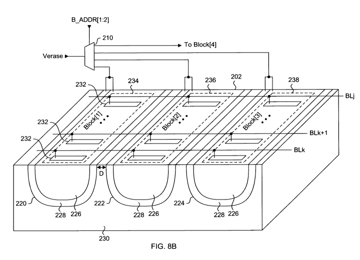
[0038] Figure 8A shows a NAND flash memory bank according to an example of
the NAND flash memory bank embodiment of Figure 6.. The NAND flash memory bank
has reduced substrate capacitance. Referring to Figure 8A, one NAND flash
memory
bank 200 has a memory array 202 including NAND cell strings similar to those
shown in
Figure 2. The NAND flash memory bank 200 has also a row decoder 204 for
driving
wordlines connected to the devices of the NAND cell strings, and a page buffer
206
connected to bitlines for coupling read and program data to the NAND cell
strings. A
charge pump 208 generates the erase voltage Verase, which is provided to a
selector
210. In the illustrated example, the memory array 202 has four different well
sectors, each
selectively receiving Verase during a block erase operation. Each of the four
well sectors
includes exactly one memory block, referred to as Block[1], Block[2], Block[3]
and
Block[4]. Accordingly, a two-bit block address B ADDR[1:2] is used for
selecting one of
four memory blocks, and row decoder 204 includes the appropriate logic for
decoding the
two-bit block address B ADDR[1:2]. The same block address is received by
selector 210
for passing Verase to the well sector which includes the corresponding
selected memory
block. Selector 210 can be implemented as a 1 to 4 demultiplexor responsive to
a two-bit
control or address signal.
[0039] Figure 8B is a cross-sectional diagram of memory array 202 taken along
line B-B' in Figure 8A, and angled to show specific features on its surface.
In Figure 8B,
only the first three well sectors 220, 222 and 224 are shown, where each well
sector
includes a p-type well 226 formed within an n-type isolation well 228, the n-
type isolation
well 228 being formed within a p-type substrate 230. Both the n-type isolation
well 228
and the p-type well 226 are ion implanted regions having two-dimensional
surface areas
on the chip formed through well known masking steps that delineate their
specific shapes.
Because the substrate 230 is p-type, the n-type isolation wells 228 are used
to electrically
isolate the p-type substrate 230 from the p-type wells 226. The depth and
concentration
of wells 226 and 228 is determined by the ion implantation energy and dose,
which are
both fabrication design parameters of the semiconductor device. As clearly
shown in
Figure 8B, the NAND cell strings are formed in the p-type wells 226. In an
alternate
example where substrate 230 is n-type instead of p-type, the n-type isolation
wells 228
-15-
CA 02701625 2010-03-30
WO 2009/086618 PCT/CA2008/002287
are omitted, and the well sectors 220, 222 and 224 have p-type wells 226.
According to
the present examples, each well sector includes at least the device well the
NAND cell
strings are formed within, and optionally includes isolation wells for
isolating the substrate
230 from the device wells 226.
[0040] In the presently shown example of memory array 202, well sectors 220,
222 and 224 include memory blocks 234, 236 and 238 respectively. Each memory
block
includes NAND cell strings 232 electrically coupled to respective bitlines,
such as bitlines
BLk and BLk+1 to BLj for example. While not shown in Figure 8B, the bitlines
are
connected to a page buffer for sensing cell data and for providing program
data. The
possible circuit implementations of page buffers, and their operation should
be well
known to persons of skill in the art. The selector 210 is shown in Figure 8B
to show its
interconnection with the well sectors 220, 222 and 224 of memory array 202.
Selector
210 receives Verase and electrically couples Verase to one of the four well
sectors in
response to the two-bit block address B ADDR[1:2]. As shown in Figure 813,
each output
of selector 210 is connected to a respective p-type well 226 as well as its
corresponding
isolation well 228. This is to ensure that the junction between the p-type
substrate 230
and the n-type isolation well 228 is reverse biased.
[0041] The advantage of having separate well sectors for each memory block of
the memory bank is the reduced capacitive loading of the charge pump relative
to the
single well memory bank of the known NAND flash memory bank of Figure 3. An
example
comparison between the single well memory bank of Figure 3 and the multiple
well sector
example of Figures 8A and 8B follows. It is first assumed that the memory bank
of Figure
3 and the memory bank of Figure 8A include exactly four memory blocks, have
the same
number of NAND cell strings per memory block, and the same charge pump
fabricated
with the same process and technology node. As previously discussed, t delay is
the
amount of time p-type well 54 charges up from VSS to Verase during an erase
operation
for erasing one memory block. In the NAND flash memory bank of Figure 8A/8B,
the
capacitance of one p-type well 226 is effectively 1/4 that of p-type well 54.
Accordingly,
the voltage level of p-type well 226 will rise from VSS to Verase in less time
than t delay.
Alternatively, if the erase time of the memory bank of Figure 3 is to be
maintained for the
NAND flash memory bank of Figure 8A, then the charge pump circuit capacity can
be
decreased. This can be done through a combination of reducing the size of
capacitor
elements and/or eliminating entire capacitor elements. Therefore semiconductor
chip
area is reduced, and the cost of the NAND flash memory device is
correspondingly
-16-
CA 02701625 2010-03-30
WO 2009/086618 PCT/CA2008/002287
reduced. Furthermore, since the capacitance of each well sector is smaller
than that of p-
type well 54, significant power savings is realized.
[0042] A further advantage of the NAND flash memory bank of Figure 8A and 8B
is that unselected memory blocks do not receive Verase, thereby eliminating
erase
disturb in the unselected memory blocks. This is because each memory block of
Figures
8A and 8B resides in its own well sector. Accordingly, the wordlines in the
unselected
memory blocks residing in unselected well sectors do not self-boost, and are
allowed to
float at about the VSS voltage level.
[0043] An erase operation executed upon the example NAND flash memory bank
of Figures 8A and 8B is now described with reference to the memory block drive
circuit
122 shown in Figure 7B. In the erase operation for the example of Figures 8A
and 8B,
one memory block is selected while other blocks remain unselected. In
otherwords, one
memory block is enabled while remaining memory blocks are disabled. In the
present
example erase operation, it is assumed that only memory block Block[1] is to
be erased.
Accordingly, the operation of memory block drive circuit 122 is described,
while the
operation of memory block drive circuit 124 is described for any one of the
unselected
memory blocks. To select a memory block for erasure, LTCH_EN and BA[1:4] of
memory
block drive circuit 122 will be at the high logic level, thereby setting the
level shifter circuit
to output high voltage Vh. Therefore, all the pass transistors 154 of wordline
driver circuit
128 are turned on. The row drive signals S1 to Si are driven to VSS while row
drive
signals SS and GS are floated, and the selected well sector having the
selected memory
block is biased to Verase. Memory block drive circuit 124 for an unselected
memory block
will have its corresponding block decoder circuit output set to output low
voltage Vn.
Therefore, all the pass transistors 154 corresponding to the unselected memory
blocks
will be turned off. Accordingly, the wordlines, SSL and GSL for the unselected
memory
blocks will float at approximately VSS, since these lines are typically biased
to VSS after
any read or program operation.
[0044] Table 1 below summarizes example biasing conditions during an erase
operation for a selected memory block and an unselected memory block, where
the
selected memory block resides in one well sector and the unselected memory
block
resides in a different well sector. A memory block is selected by providing
the block
address B ADDR[1:2] of the selected memory block to row decoder 204, which is
decoded to enable control of the wordlines and select lines (SSL and GSL)
corresponding
-17-
CA 02701625 2010-03-30
WO 2009/086618 PCT/CA2008/002287
to the selected memory block. Because B ADDR[1:2] is received by selector 210,
Verase
is passed to the well sector which includes the selected memory block.
[0045] Table 1
Selected Well Sector Unselected Well Sector
Selected Memory Block Unselected Memory
Block
Bitlines (B/L) Clamped to Verase- Clamped to Verase-
0.6V 0.6V
String Select Line Floated Unselected
(SSL)
Wordlines OV Unselected
Ground Select Line Floated Unselected
(GSL)
Common Source Line Clamped to Verase- OV
(CSL) 0.6V
P-Well Verase OV
[0046] In order to erase a selected memory block in the example NAND flash
memory bank of Figures 8A and 8B, the wordlines are biased to VSS, or OV, the
common
source line CSL (hereinafter referred to as "CSL line") is clamped to about
Verase-0.6V,
and SSL and GSL are left to float. Decoded row drive signals SS and GS for the
SSL and
GSL lines are floated during erase to minimize the electric field on pass
transistors for
SSL and GSL. It is noted that the capacitance of drive lines SS and GS are
much larger
than that of SSL and GSL. Therefore, SSL and GSL may remain at nearly VSS
because
any boosted charge on SSL and GSL resulting from the well voltage rising to
Verase will
leak through the pass transistors to the SS and GS drive lines.
[0047] Finally, the selected well sector within which the selected memory
block
resides is biased to Verase. Under these conditions, trapped charge in the
floating gates
of the flash memory cells of the NAND cell strings will emit their charge to
the well. As
previously shown in Figure 2 and Figure 4, all bitlines are shared by the
memory blocks in
the memory bank, and have bitline contacts electrically connected to the n+
diffusion
region 88 corresponding to each NAND cell string. The n+ diffusion regions 88
are
forward biased when the selected well sector is raised to the erase voltage
Verase,
resulting in the bitlines being clamped to Verase-0.6V. As previously shown in
Figure 2
and Figure 4, the CSL line is shared by all the NAND cell strings in the same
memory
block via n+ diffusion region 82. Hence when the selected well sector is
raised to Verase,
-18-
CA 02701625 2010-03-30
WO 2009/086618 PCT/CA2008/002287
the n+ diffusion region 82 is forward biased raise and clamp the CSL line of
the selected
memory block in the selected well sector to Verase-0.6V. On the other hand,
the CSL line
for an unselected memory block in an unselected well sector is biased to VSS
or OV. It is
noted that in the present examples, the CSL line is common only to the NAND
cell strings
of one memory block. All wordlines, string select lines (SSL) and ground
select lines
(GSL) in the unselected memory block remain in an unselected state, meaning
that the
pass transistors 154 in the wordline driver 128 are turned off.
[0048] Figures 8A and 8B illustrate an example NAND flash memory bank where
there is exactly one memory block per well sector in memory bank array 202.
Depending
on the fabrication process and technology node being used for manufacturing
NAND
flash memory bank 200, adjacent well sectors are spaced from each other by a
minimum
distance "D", as shown in Figure 8B. This minimum distance D can be set to be
the
minimum design rule spacing for adjacent n-type isolation wells. By example
only, the
spacing between adjacent n-type isolation wells 228 can be between 3 to 10
microns.
[0049] In another example of memory array 202, each well sector of the memory
bank includes more than one memory block to minimize the size of the memory
array
while reducing the capacitance of each well sector. Figure 9A is a block
diagram of a
NAND flash memory bank with reduced memory array area relative to the example
NAND
flash memory bank of Figure 8A. Referring to Figure 9A, one NAND flash memory
bank
300 has a memory array 302 including NAND cell strings similar to those shown
in Figure
2, a row decoder 304 for driving wordlines connected to the devices of the
NAND cell
strings, and a page buffer 306 connected to bitlines for coupling read and
program data to
the NAND cell strings. A charge pump 308 generates the erase voltage Verase,
which is
provided to a selector 310. By example only, the illustrated NAND flash memory
bank has
a memory array 302 including two different well sectors, each selectively
receiving
Verase during a block erase operation. Memory array 302 includes four memory
blocks,
referred to as Block[1], Block[2], Block[3] and Block[4]. Accordingly, a two-
bit block
address B_ADDR[1:2] is used for selecting one of four memory blocks and row
decoder
304 includes the appropriate logic for decoding the two-bit block address B
ADDR[1:2].
[0050] In the memory array 302, a first well sector includes memory blocks
Block[1] and Block[2], and a second well sector includes memory blocks
Block[3] and
Block[4]. A pair of two well sectors is selected during an erase operation. A
single bit
block address signal is received by selector 310 for passing Verase to the
well sector
which includes the selected memory block. If B_ADDR[1] is the most significant
block
-19-
CA 02701625 2010-03-30
WO 2009/086618 PCT/CA2008/002287
address bit for selecting which pair of memory blocks is to be selected, then
B ADDR[2]
is the least significant block address bit for selecting one memory block of
the selected
pair of memory blocks. Selector 310 is a 1-to-2 demultiplexor, or selector,
responsive to a
single-bit control or address signal. Because the example of Figure 9A has two
memory
blocks formed in each well sector, only one of the two well sectors is
selected for any
memory block erase operation. Therefore block address B ADDR[1] is used by
selector
310 for passing Verase to one of the two well sectors. In otherwords, selector
310
receives a portion of the block address for selectively passing Verase to one
of the two
well sectors.
[0051] Figure 9B is a cross-sectional diagram of memory array 302 of Figure 9A
taken along line C-C', and angled to show specific features on its surface. In
Figure 9B,
two well sectors 320 and 322 are shown, where each well sector includes a p-
type well
324 formed within an n-type isolation well 326, the n-type isolation well 326
being formed
within a p-type substrate 328. Both the n-type isolation well 326 and the p-
type well 324
are ion implanted regions having two-dimensional surface areas on the chip
formed
through well known masking steps that delineate their specific shapes. The
depth and
concentration of wells 226 and 228 is determined by the ion implantation
energy and
dose, which are both fabrication design parameters of the semiconductor
device. As
clearly shown in Figure 9B, the NAND cell strings are formed in the p-type
wells 324. In
an alternate example where substrate 328 is n-type instead of p-type, the n-
type isolation
wells 326 are omitted, and the well sectors 320 and 322 have p-type wells 324.
According
to the present examples, each well sector includes at least the device well
the NAND cell
strings are formed within, and optionally includes isolation wells for
isolating the substrate
from the device wells.
[0052] In the presently shown example of memory array 302, well sector 320
includes memory blocks 330 and 332, which correspond to memory blocks Block[1]
and
Block[2] respectively. Well sector 322 includes memory blocks 334 and 336,
which
correspond to memory blocks Block[3] and Block[4] respectively. Each memory
block
includes NAND cell strings 338 electrically coupled to respective bitlines,
such as bitlines
BLk and BLk+1 to BLj for example. While not shown in Figure 9B, the bitlines
are
connected to a page buffer for sensing cell data and for providing program
data. The
possible circuit implementation of page buffers, and their operation should be
well known
to persons of skill in the art. The selector 310 is shown in Figure 9B to show
its
interconnection with the well sectors 320 and 322 of memory array 302.
Selector 310
receives Verase and electrically couples Verase to one of the two well sectors
in
-20-
CA 02701625 2010-03-30
WO 2009/086618 PCT/CA2008/002287
response to the single-bit block address B ADDR[1 ]. As shown in Figure 9B,
each output
of selector 310 is connected to a respective p-type well 324 as well as its
corresponding
isolation well 326.
[0053] The erase operation for a selected memory block in the example NAND
flash memory bank of Figures 9A and 9B is similar to that described for the
example
NAND flash memory bank of Figures 8A and 8B, except that an erase inhibit
scheme is
applied to the unselected memory block of the selected well sector that
receives the
erase voltage Verase. This is due to the fact that each well sector has both a
selected
memory block to be erased and an unselected memory block. Therefore, the flash
memory cells of the unselected memory block in the well sector receiving
Verase is erase
inhibited. By example, the previously described self-boosting erase inhibit
scheme can be
used for inhibiting erasure of the flash memory cells of the unselected memory
block in
the selected well sector, where a selected well sector is the one that
receives Verase. For
example, if memory block 332 (Block[2]) is selected for erasure, then the
wordlines and
select lines (SSL and GSL) corresponding to selected memory block 332 are
biased to
the erase condition, and Verase is applied to well sector 320. Memory block
330 is erase
inhibited to prevent erasure of its flash memory cells because it is formed
within the same
p-type well 324 as memory block 332.
[0054] Table 2 summarizes example biasing conditions during an erase operation
for a selected memory block and an unselected memory block in the selected
well sector
that receives Verase, and for unselected memory blocks in an unselected well
sector that
does not receive Verase.
[0055] Table 2
Selected well sector Unselected well
sector
Selected Memory Unselected All Memory Blocks
Block Memory Blocks
Bitlines (BL) Clamped to Clamped to Verase Clamped to Verase
Verase -0.6V -0.6V -0.6V
String Select Line Floated Boosted to about Unselected
(SSL) 90% of Verase
Wordlines (WLO - OV Boosted to about Unselected
WL31) 90% of Verase
Ground Select Line Floated Boosted to about Unselected
(GSL) 90% of Verase
Common Source Line Clamped to Clamped to Verase OV
(CSL) Verase -0.6V -0.6V
-21 -
CA 02701625 2010-03-30
WO 2009/086618 PCT/CA2008/002287
Well sector Verase Verase OV
[0056] The erase bias conditions for the word lines and SSL and GSL are the
same as for the NAND flash memory bank examples of Figures 8A, 8B and Figures
9A,
913, as are the bias conditions for the unselected memory blocks in the
unselected well
sectors. However, for the unselected memory blocks of the selected well
sector, the
wordlines are self boosted to about Verase. When the wordlines are
approximately
Verase, there is a minimal electrical field formed between the wordlines and
the p-type
well 324 of the selected well sector, thereby inhibiting erasure of the flash
memory cells of
the unselected memory block.
[0057] While Figures 8A, 8B and 9A, 9B show examples where there is exactly
one memory block formed per well sector and two memory blocks formed per well
sector
in one memory array, alternate examples can include any number of well sectors
in each
memory array, where each well sector can include any number of memory blocks
formed
therein.
[0058] In both the example NAND flash memory banks of Figures 8A, 8B and 9A,
9B, the voltage of the bitlines rises to about Verase-0.6V when the p-type
well of the well
sector rises to Verase. With reference to Figure 4 for example, the p-type
well 54 and the
n+ diffusion region 88 has a p-n junction that is forward biased when Verase
is applied.
Accordingly, bitline 90 will clamp to about Verase-0.6V, where 0.6V is the
forward bias
voltage drop across the p-n junction. Each bitline is electrically connected
to the NAND
cell strings in each memory block of the memory array. Accordingly, this
clamped voltage
of the bitline is applied to the n+ diffusion regions 88 of all the NAND cell
strings of the
column, and notably to the n+ diffusion regions 88 of the NAND cell strings in
the
unselected well sectors. Since the unselected well sectors are biased to VSS,
or float
near VSS, the bitlines potentially provide a charge leakage path between the
selected
well sector and one or more unselected well sectors. More specifically, Verase
being
applied to the selected well sector can be discharged to VSS through the
unselected well
sector if junction breakdown occurs at the p-n junctions of the n+ diffusion
region 88 and
the p-type well 54 of each NAND cell string. This can delay the rise of Verase
in the
selected well sector, or even disrupt the erase process if the selected well
sector voltage
never fully reaches Verase. With this understanding of the bitline voltage
during erase
operations, the junction breakdown voltage of the n+ diffusion region 88 is
engineered to
withstand breakdown when the bitline rises to Verase-0.6V.
-22-
CA 02701625 2010-03-30
WO 2009/086618 PCT/CA2008/002287
[0059] Although junction breakdown engineering is a possible solution to this
problem, a simpler solution is to electrically isolate the bitline connected
to the selected
well sector from the unselected well sectors. According to a present
embodiment, since
well sectors are spaced from each other due to design rules, an isolation
device is
included in-line with the bitline between well sectors. Figure 10 illustrates
an example of
this embodiment.
[0060] Figure 10 is another example of the memory array 302 shown in Figures
9A and 9B. In Figure 10, memory array 400 has the same elements as those shown
in
Figure 9B. In order to isolate the bitlines connected to one well sector from
the NAND cell
strings of another well sector, isolation devices, such as n-channel
transistors 402 are
formed in the space between well sectors. The n-channel transistors 402 can be
formed
as high voltage transistor devices, at the same time other high voltage
transistor devices
are formed on the memory device. The bitlines electrically connected to the
NAND cell
strings of one well sector are connected to one terminal of isolation devices
402, while the
bitlines electrically connected to the NAND cell strings of an adjacent well
sector are
connected to the other terminal of isolation devices 402. Therefore, the
bitlines connected
to the NAND cell strings in one well sector are referred to as bitline
segments. In Figure
10, these bitline segments are indicated by reference numbers 404. If there
are more
than two well sectors in memory array 400, then there are additional isolation
devices 402
connected in-line or in series, with each bitline segment 404. The gate
terminals of all the
isolation devices 400 receive a bias voltage Viso, which is selected to be at
least a
voltage level sufficiently high for passing the highest voltage level that is
applied to the
bitline during read and program operations. The isolation devices are hence
enabled
during a read or program operation. In otherwords, the gate terminals of all
the isolation
devices can be overdriven to a level above the supply voltage VDD. There may
be
devices where overdriving the gate terminals is not necessary, and it is
sufficient to drive
them to the supply voltage VDD.
[0061] For example, if VDD is applied to bitlines during a programming
operation
for programming a particular logic state to a flash memory cell, then the bias
voltage Viso
should be at least VDD+Vtn, where Vtn is a threshold voltage of an n-channel
transistor.
By setting Viso to such a voltage level, a full VDD voltage level is
maintained in all bitline
segments during programming. During an erase operation for a memory block in a
selected well sector, the corresponding bitline segment will rise to about
Verase-0.6V. But
because the isolation devices 404 have their gates biased to Viso = VDD+Vtn,
the other
bitline segments are limited to being charged to VDD. Therefore, minimal
additional
-23-
CA 02701625 2010-03-30
WO 2009/086618 PCT/CA2008/002287
junction breakdown engineering is required since the n+ diffusion region
connected to the
bitlines is already designed to withstand a VDD voltage level.
[0062] In one example of the memory array 400, Viso is statically maintained
at
the same voltage level during read, program and erase operations. Persons
skilled in the
art should understand that there are different ways to provide Viso. In an
alternate
example Viso can be a decoded signal, meaning that Viso is selectively applied
to the
gates of the isolation devices adjacent to the selected well sector.
[0063] Figure 11 is a circuit schematic of an example of the embodiment of
Figure
10. In Figure 11, one memory bank has a memory array with dynamically
activated
isolation devices formed between well sectors for defining bitline segments,
and a bitline
segment decoder for selectively isolating one bitline segment from the other
bitline
segments in each column. The row decoder is not shown in order to simplify the
schematic, but those skilled in the art will understand that they are
necessary for driving
the wordlines of the NAND cell strings in each memory block. A memory bank 500
includes a memory array 502, a page buffer 504 and a bitline segment decoder
506.
Memory array 502 of the present example includes four well sectors 508, 510,
512 and
514, where each well sector includes exactly one memory block. Accordingly,
memory
array 502 has the same structure as memory array 202 of Figures 8A/8B. Formed
between each well sector are isolation devices 516, each being an n-channel
transistor
for the present example. Bitline segments 518 are connected to the NAND cell
strings in
each memory block, and are connected to an isolation device at both ends.
Bitline tail
segments 520 and 522 are bitline segments which are not connected to any NAND
cell
strings and are connected to one isolation device 516 and some other
terminating circuit.
For example, bitline tail segments 520 are connected to isolation devices 516
above well
sector 508 and to a bitline precharge circuit 524. Bitline tail segments 522
on the other
hand are connected to isolation devices 516 below well sector 514 and to page
buffer
504. While the present example of Figure 11 shows each well sector having one
memory
block formed therein, according to alternate examples each well sector can
have multiple
memory blocks formed therein, where a bitline segment is commonly connected to
the
multiple memory blocks residing in the same well sector. The isolation devices
516 driven
by NAND logic gate 532 and NAND logic gate 540 are optional, meaning that the
bitline
segments 518 corresponding to well sectors 508 and 514 can extend to the
precharge
circuit 524 and the page buffer 504 respectively.
-24-
CA 02701625 2010-03-30
WO 2009/086618 PCT/CA2008/002287
[0064] Bitline segment decoder 506 is responsible for disabling, rendering
electrically non-conductive, or turning off, the selected isolation devices
516 for isolating a
bitline segment 518 corresponding to a selected well sector including the
selected
memory block to be erased, from all other bitline segments 518. Bitline
segment decoder
506 includes OR logic gates 526, 528 and 530, and NAND logic gates 532, 534,
536, 538
and 540. Each of OR logic gates 526, 528 and 530 receives two different well
sector
selection signals, and more specifically, two well sector selection signals
corresponding to
adjacent well sectors. Because adjacent well sectors share the same isolation
device
516, an OR logic gate is used to disable the isolation devices 516 between two
adjacent
well sectors when either is selected or addressed for an erase operation. In
the example
of Figure 11, the well sector selection signals correspond to decoded block
address
BA[1:4] because there is exactly one memory block in each well sector. The
number of
well sector selection signals required by bitline segment decoder 506 depends
on the
number of well sectors in the memory array of the memory bank. For example, if
there
were exactly two memory blocks in each well sector of Figure 11, then there
are a total of
eight (8) memory blocks. Accordingly, three block address signals are used for
individually selecting one of eight memory blocks, but two of the most
significant block
address signals can be used for generating the well sector selection signals.
For
example, a modified version of the memory block drive circuit 122 of Figure 7B
can have
a three input AND logic gate instead of the 2 input AND logic gate 140 for
decoding
B ADDR[1], B ADDR[2] and B ADDR[3] to perform a one of eight selection.
Accordingly,
persons skilled in the art will understand that there would be a total of
eight memory block
drive circuits, one for each memory block. In the present example, the two
most
significant block addresses B ADDR[3] and B ADDR[2] are decoded using well
known
logic to provide four well sector selection signals.
[0065] NAND logic gates 534, 536 and 538 each have a first input for receiving
the output of OR logic gates 526, 528 and 530 respectively. NAND logic gate
532 has a
first input for receiving a well sector selection signal directly because the
isolation devices
516 above well sector 508 are not shared with another well sector. Similarly,
NAND logic
gate 540 has a first input for receiving a well sector selection signal
directly because the
isolation devices 516 below well sector 514 are not shared with another well
sector. The
second input of all the NAND logic gates receives an erase signal ERASE, and
the output
of each NAND logic gate drives a set of isolation devices 516 adjacent to at
least one well
sector. The high logic level output of each NAND logic gate is set such that
the isolation
devices 516 are driven to a voltage level sufficient to allow the maximum
bitline voltage
-25-
CA 02701625 2010-03-30
WO 2009/086618 PCT/CA2008/002287
level to pass through it. For example, if the maximum bitline voltage is VDD
then the
NAND logic gates are supplied with a positive voltage higher than VDD.
[0066] According to the present example, signal ERASE is set to the low logic
level for a read or program operation, thereby turning on or overdriving all
the isolation
devices 516. As previously stated all the NAND logic gates can be supplied
with a voltage
level greater than the VDD supply voltage. Therefore the logic states of the
well sector
selection signals BA[1:4] are ignored. During an erase operation, signal ERASE
is set to
the high logic level. Now NAND logic gates 532 and 540 are responsive to the
well sector
selection signals BA[1:4], and NAND logic gates 534, 536 and 538 are
responsive to an
output of a corresponding OR logic gate. The NAND logic gates are responsive
by driving
their outputs to the inactive logic level when their first and second inputs
are both at the
high logic level. Accordingly, when one well sector selection signal is at the
active high
logic level, the sets of isolation devices adjacent to the correspondingly
selected well
sector are turned off. Then the erase voltage Verase is applied to the
selected well
sector.
[0067] For example, if a memory block in well sector 510 is to be erased, then
only address BA[2] is driven to the high logic level. Then NAND logic gates
534 and 536
drive their respective outputs to the low logic level, such as VSS, and the
isolation
devices 516 having their gates electrically coupled to the outputs of NAND
logic gates
534 and 536 will turn off. Therefore, the bitline segments 518 of well sector
510 are
isolated from the other bitline segments of the other well sectors.
[0068] In the example of Figure 11, bitline segments 518 are selectively
disconnected from the other bitline segments in response to decoded block
addresses
BA[1:4] during an erase operation. In an alternate example, all the isolation
devices are
globally enabled and disabled in response to the operating mode of the memory
device.
More specifically, if an erase operation is executed, then all the isolation
devices 516 are
turned off independently of any address information.
[0069] Figure 12 is a circuit schematic of one memory bank having a memory
array with dynamically activated isolation devices formed between well
sectors, according
to an alternate example of the embodiment of Figure 10. In Figure 12, memory
bank 550
includes the same memory array 502 shown in Figure 11, but now bitline segment
decoder 506 is replaced with a simple segment decoupling logic 552. Segment
decoupling logic 552 includes inverters 554, 556, 558, 560 and 562, each of
which
receives the erase signal ERASE in parallel, and drives a respective set of
isolation
-26-
CA 02701625 2010-03-30
WO 2009/086618 PCT/CA2008/002287
devices 516. In the present example, the inverters are provided with a supply
voltage
VDD or a voltage level greater than VDD to overdrive the isolation devices 516
during
non-erase operations. In an erase operation, signal ERASE is driven to the
high logic
level, and all the inverters drive the gates of the isolation devices 516 to
VSS. All the
isolation devices 516 turn off, resulting in all the bitline segments 518
being isolated from
each other, and Verase is applied to the selected well sector that includes
the memory
block to be erased. In a program or read operation, ERASE is at the low logic
level, and
the isolation devices have their gates driven to a voltage level of at least
VDD.
[0070] In both the examples of Figures 11 and 12, ERASE is at the inactive low
logic level during a read or program operation to ensure that all the
isolation devices 516
are at least turned on, or overdriven. Unfortunately, a known issue affecting
sensing time
is bitline capacitance. Those skilled in the art understand that as the
bitline length
increases, its capacitance increases as well. Because the current through a
conducting
flash memory cell is small, this current is difficult to sense when the
bitline capacitance is
high. Therefore, the isolation devices shown in Figures 11 and 12 can be used
in an
alternate embodiment of the invention to reduce bitline capacitance to shorten
sensing
time.
[0071] Figure 13 is a circuit schematic of an alternate memory bank 570
according to an example of the embodiment for reducing bitline capacitance to
shorten
sensing time. Memory array 502 is the same as the one shown in Figure 11, but
an
alternate bitline segment decoder 572 according to an example of the present
embodiment is illustrated. Bitline segment decoder 572 turns off all the
isolation devices
516 in memory array 502 during an erase operation, and selectively turns off
specific
isolation devices 516 during a read operation. In Figure 13, bitline segment
decoder 572
includes an inverter 574 having its output for providing an isolation drive
signal coupled to
a respective set of isolation devices 516 between the bitline precharge
circuit 524 and
well sector 508, and OR logic gates 576, 578, 580 and 582 each having an
output for
providing an isolation drive signal coupled to respective sets of isolation
devices 516. A
first input of OR logic gates 576, 578, 580 and 582 is coupled to the outputs
of NOR logic
gates 584, 586, 588 and 590 respectively. Inverter 574 and each pairing of a
NOR logic
gate and OR logic gate are referred to as an isolation device driver, having
outputs for
driving respective isolation devices. A second input of OR logic gates 578,
580 and 582
receives the output of another isolation device driver, while the second input
of OR logic
gate 576 is grounded. Each isolation device driver provides its isolation
drive signal for
one set of isolation devices 516 to one isolation device driver that provides
its isolation
-27-
CA 02701625 2010-03-30
WO 2009/086618 PCT/CA2008/002287
drive signal to a second set of isolation devices 516, where the second set of
isolation
devices is located between the first set of isolation devices and the page
buffer 504. A
first input of OR logic gates 584, 586, 588 and 590 receives the erase signal
ERASE. A
second input of NOR logic gates 584, 586, 588 and 590 is an inverted input,
and receives
well sector selection signals BA[1], BA[2], BA[3] and BA[4] respectively.
[0072] As previously mentioned for the example arrangement of memory array
502, each well sector includes one memory block, hence decoded block addresses
BA[1:4] can be used as the well sector selection signals. The operation of
bitline segment
decoder 572 is straightforward during an erase operation. Signal ERASE is set
to the
active high logic level, thereby causing each NOR logic gate to provide a low
logic level
output which is passed by each OR logic gate as the isolation drive signal to
all the
isolation devices 516. Therefore all the isolation devices 516 are turned off
while ERASE
is at the high logic level, and Verase can be applied to the selected well
sector.
[0073] During a read operation, only the isolation devices 516 located between
the well sector containing the selected memory block and the page buffer 504
are turned
on, or overdriven. All other isolation devices are turned off to minimize the
bitline
capacitance seen by the selected NAND cell strings of the selected memory
block. For
example, when a memory block in well sector 512 is selected for a read
operation,
isolation devices 516 between well sectors 512 and 514 are turned on, as are
the
isolation devices 516 between well sector 514 and page buffer 504. Therefore
during a
read operation for a selected memory block, only the bitline segments 518
corresponding
to the selected well sector including the selected memory block, and the
bitline segments
518 corresponding to all the other intervening well sectors between the
selected well
sector and the page buffer are electrically coupled to each other. In the
example of Figure
13, each OR logic gate of the isolation device driver is an address overrider
circuit. It is
noted that the isolation device driver having inverter 574 does not include a
NOR logic
gate and an OR logic gate, since there are no further well sectors between the
isolation
devices 516 it controls and bitline precharge circuit 524. The address
overrider circuit
allows for an isolation device driver activated by a well sector selection
signal to enable or
activate the next set of isolation devices 516 proximate to the page buffer
504.
[0074] In an example read operation the selected memory block resides in well
sector 510, thus BA[2] is driven to the high logic level and ERASE is at the
low logic level.
With ERASE at the low logic level, inverter 574 turns on or overdrives its
isolation
devices. NOR gate 584 provides a low logic level output since BA[1] is at the
low logic
-28-
CA 02701625 2010-03-30
WO 2009/086618 PCT/CA2008/002287
level, which is passed by OR gate 576 to its respective set of isolation
devices 516. NOR
gate 586 provides a high logic level output to OR gate 578, which also
receives the low
logic level output from OR gate 576. Accordingly, the isolation devices 516
between well
sectors 510 and 512 are turned on or overdriven. With BA[3] at the low logic
level, NOR
gate 588 drives its output to the low logic level. However, the high logic
level output of OR
gate 578 is received by OR gate 580. Therefore the output of NOR gate 588 is
overridden. Similarly, the output or NOR gate 590 is overridden by OR gate
582, thus the
isolation devices 516 between well sectors 512 and 514 and page buffer 504 are
turned
on.
[0075] With the reading scheme shown in Figure 13, the worst case read
situation
occurs when the selected memory block resides within well sector 508, which is
the
furthest from page buffer 504. On the other hand, the best case read situation
occurs
when the selected memory block resides within well sector 514, which is the
closest to
page buffer 504. Therefore, the sense timing and data output transfer timing
can be
adjusted based on the selected well sector that includes the selected memory
block to be
read. In one example application, a specific number of the memory blocks
formed in well
sectors proximate to the page buffer 504 can be designated as high speed
memory
blocks. The remaining memory blocks residing in the well sectors further from
the page
buffer 504 can be designated as regular speed memory blocks. While in use with
an
external system, data can be selectively stored in either high speed or
regular speed
memory blocks for high speed or regular speed read operations.
[0076] Figure 14 is a flow chart summarizing the method by which a selected
memory block is erased, in accordance with the previously described
embodiments of the
invention. The following method is applicable to a memory array having any
number of
well sectors, where each well sector includes at least one memory bank.
Starting at step
600 a selected memory block is biased for erasing, which is done by setting
the
wordlines, SSL and GSL to the appropriate erase bias conditions. Table 2
illustrates
example erase bias conditions for the memory block to be erased. If each well
sector
includes at least two memory blocks, then there is an unselected memory block
in the
same well sector as the selected memory block to be erased. Therefore at step
602, the
unselected memory block in the same well sector as the selected memory block
is biased
to inhibit erase of its memory cells. Once again, Table 2 illustrates example
erase inhibit
bias conditions for the wordlines, SSL and GSL. If on the other hand each well
sector
includes exactly one memory block, then step 602 is skipped. Proceeding to
step 604, the
erase voltage is applied to the well sector containing the selected memory
block.
-29-
CA 02701625 2010-03-30
WO 2009/086618 PCT/CA2008/002287
Following at step 606, the bitline segments of the selected well sector are
decoupled from
the other bitline segments either at the same time or just after Verase is
applied to the
selected well sector. It is noted that it is sufficient to decouple the
bitline segment of the
selected well sector from the bitline segments of adjacent well sectors. This
decoupling is
either dynamic decoupling or static decoupling. Static decoupling occurs when
the
isolation devices are statically biased to Viso, and the bitline segments of
the selected
well sector self-decouple from the other bitline segments as its voltage rises
past Viso.
Dynamic decoupling occurs by actively turning off the isolation devices either
globally in
response to a single control signal, such as ERASE, or in response to a well
sector
selection signal. If dynamic decoupling is used, then the isolation devices
can be turned
off prior to application of Verase to the selected well sector.
[0077] The presently shown memory bank embodiments and examples of the
invention reduce power consumption while improving the speed at which a memory
block
is erased by forming well sectors that can be selectively biased to the
required erase
voltage. Each well sector has at least one memory block formed therein, and
thus has a
lower capacitance than prior art NAND flash memory arrays that have all memory
blocks
formed in one large well. All the previously described memory bank embodiments
and
examples can be used in the NAND memory device of Figure 1A, or the NAND
memory
device chip of Figure 1 B.
[0078] As shown by the previous embodiments and examples, a memory array of
a memory bank will have reduced well capacitance by forming at least two well
sectors,
each well sector having at least one memory block formed therein. The reduced
well
capacitance allows for higher erase speeds for the selected memory block than
prior art
single well memory arrays. If erase performance is a non-critical
specification for the
NAND flash memory device having multiple well sectors in its memory bank, the
charge
pump size can be reduced while maintaining erase speeds similar to that of
prior art
NAND flash memory devices. In the embodiments and examples described above,
the
device elements are connected to each other as shown in the figures, for the
sake of
simplicity. In practical applications of the present invention to an
apparatus, devices,
elements, circuits, etc. may be connected directly to each other. As well,
devices,
elements, circuits etc. may be connected indirectly to each other through
other devices,
elements, circuits, etc., necessary for operation of the apparatus. Thus, in
actual
configuration, the circuit elements and devices are directly or indirectly
coupled with, or
connected to, each other.
-30-
CA 02701625 2010-03-30
WO 2009/086618 PCT/CA2008/002287
[0079] In the preceding description, for purposes of explanation, numerous
details
and examples are set forth in order to provide a thorough understanding of the
embodiments of the invention. However, it will be apparent to one skilled in
the art that
these specific details are not required in order to practice the invention. In
other
instances, well-known electrical structures and circuits are shown in block
diagram form
in order not to obscure the invention. For example, specific details are not
provided as to
whether the embodiments of the invention described herein are implemented as a
software routine, hardware circuit, firmware, or a combination thereof.
[0080] The above-described embodiments of the invention are intended to be
examples only. Alterations, modifications and variations can be effected to
the particular
embodiments by those of skill in the art without departing from the scope of
the invention,
which is defined solely by the claims appended hereto.
-31-