Note: Descriptions are shown in the official language in which they were submitted.
CA 02701874 2010-04-01
WO 2009/043725 PCT/EP2008/062383
PROCESS FOR PREPARING A SOLAR. CELL
Technical Field
The present invention relates to a process for preparing a solar cell
based on thin layers of cadmium sulfide (CdS) and cadmium telluride
(CdTe).
Background Art
Cadmium telluride is a photoactive material which has revealed itself
to be particularly suitable for manufacturing solar cells, since it is
characterized by a so-called "energy gap" with a value of 1.45 eV which is
highly favorable. Moreover, polycrystalline layers of CdTe with a thickness
of a few micrometers ( m) can be deposited easily by way of several
technologies, including Physical Vapor Deposition (PVD), Chemical Vapor
Deposition (CVD), Close-Space Sublimation (CSS), screen-printing, spray
methods and others. However, such technologies require generally a certain
type of treatment after deposition in order to optimize the properties of the
active layers of the cell.
CdTe was used for the first time in the manufacture of solar cells in
the 1960s and, at the end of the 1970s, the efficiency of such cells had
reached a value of 9%. The production process used entails doping the
CdTe by introducing oxygen in the material deposition step, working at high
temperatures (560-580 C). A post-deposition treatment in an oxygen
atmosphere also contributes to a further 1-2% increase in terms of
efficiency. However, this process has revealed itself to be scarcely
practical,
since it is scarcely controllable and expensive, especially due to the high
costs of the substrates made of heat-resistant glass required for the
procedure.
Subsequently, in the 1980s, a method for CdTe deposition of the
Closed Space Vapor Transport (CSVT) type was developed. This process
utilizes the favorable properties of the heat-resistant glass support, which
is
heated rapidly to the temperature of 650 C. The CdTe is then deposited by
CA 02701874 2010-04-01
WO 2009/043725 PCT/EP2008/062383
2
the source heated at 600 C.
Deposition methods of the electrolytic type were also developed in
the 1980s. In this case, an aqueous solution of CdSO4 and Te203 at the
temperature of 90 C is used. However, such electrolytic methods require
long times for deposition, since the deposition rate must be kept low in
order to avoid the development of fluctuations in the stoichiometry of the
CdTe layer.
Screen-printing technology instead uses a suspension of particles of
Cd and Te dust, which is deposited on the support and then converted into a
relatively thick CdTe layer by means of a thermal treatment at high
temperatures (above 700 C). In this case also, the method is expensive due
to the cost of the suitable substrates.
Deposition methods of the spray type utilize an aqueous solution of
components which contain Cd and Te, which is atomized and deposited in
the form of droplets onto the support, which is heated to 400 C. Since the
CdTe layer that is deposited tends to form porous structures, the deposition
must lead to the formation of a thick layer, which can help prevent the
subsequent permeation, within the cavities of the CdTe layer, of the material
that constitutes the layers to be deposited later. This aspect, combined with
the great quantity of material that is wasted during the atomization step,
causes spray methods to be relatively onerous.
There is, therefore, the need to develop a process for preparing a solar
cell based on CdS and CdTe in which low-cost precursors are used in
quantities which are not excessive, in which relatively low temperature
conditions are used, and which can be applied easily in the industrial sector
to allow inexpensive mass-production of solar cells.
Disclosure of the Invention
The aim of the present invention is to provide a process for preparing
solar cells based on CdS and CdTe which is inexpensive and simple to
provide.
CA 02701874 2010-04-01
WO 2009/043725 PCT/EP2008/062383
3
Within this aim, an object of the invention is to provide a process
which can be implemented easily in the industrial field.
Another object of the invention is to provide a process which is
highly reliable, relatively easy to carry out and at competitive costs.
This aim and these and other objects which will become better
apparent hereinafter are achieved by a process for preparing a solar cell
comprising a support, a layer of cadmium sulfide (CdS), a layer of cadmium
telluride (CdTe), a layer of a transparent conductive oxide (TCO), a
conductive metallic layer and optionally a layer of buffer material,
characterized in that the CdS layer and the CdTe layer are deposited by
means of a pulsed plasma deposition (PPD) method.
Moreover, the aim and objects of the invention are also achieved by a
solar cell which can be obtained according to the process of the invention.
Brief Description of the Drawings
Further characteristics and advantages of the invention will become
better apparent from the description of a preferred but not exclusive
embodiment of the process and of the solar cell according to the invention,
illustrated by way of non-limiting example in the accompanying drawings,
wherein:
Figure 1 a is a diagram of a device which works according to the PPD
method, suitable to perform the process according to the invention;
Figure I b is a view of the ablation and plasma generation effect on
the part of a PPD device on a target, in which it is possible to notice the
primary plasma of the electron pulse in the glass capillary and the secondary
plasma of material of the target created by microexplosion caused by the
arrival of the electron pulse on the surface of the target;
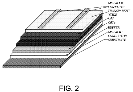
Figure 2 is a diagram of a solar cell which can be obtained according
to an embodiment of the process according to the invention;
Figure 3 is a photograph of a solar cell which can be obtained
according to an embodiment of the process according to the invention.
CA 02701874 2010-04-01
WO 2009/043725 PCT/EP2008/062383
4
Ways of carrying out the Invention
In one of its aspects, the present invention relates to the deposition of
layers of photoactive materials (CdS and CdTe) and optionally layers of
buffer materials by adapting a pulsed plasma deposition (PPD) technique
based on the generation of pulses of electrons at high energy (up to 25 k.eV)
and by the plasma created by a working gas, such as oxygen, argon or
nitrogen, at low pressure (from 10-6 to 10-2 mbar), disclosed in EP 1867221
A2, assumed included herein by reference, together with an apparatus
adapted to generate said pulses. The diagram of the apparatus used is shown
in Figure 1. Such apparatus comprises a first dielectric tube (glass bulb)
which contains a gas, a hollow cathode connected to the first tube, a second
dielectric tube (a glass tube) connected to the cathode and to a deposition
chamber within which at least one target and a support are positioned, an
anode which is arranged around the second dielectric tube, and means for
applying a voltage to the cathode and to the anode (source of high voltage
HV and capacitor bank).
The application of a suitable voltage and/or gas pressure leads to the
generation of electrons and plasma near the hollow cathode.
The electrons and the plasma are then removed and accelerated with
the electric potential difference (up to 25 kV) between the hollow cathode
and anode and pass within the second dielectric tube in an equipotential
region between the anode and the target. By means of the impact of the
pulse of accelerated electrons on the surface of a target constituted by the
material to be deposited, the energy of the pulse is transferred into the
material of the target and causes its ablation, i.e., the explosion of its
surface
in the form of a plasma of material of the target, also known as "plume",
which propagates in the direction of a support (substrate), where it is
deposited (Figure 1).
The ion conductivity of low-pressure gases ensures an electrostatic
shielding to the space charge generated by the electrons. As a consequence
CA 02701874 2010-04-01
WO 2009/043725 PCT/EP2008/062383
of this, self-sustained beams can be accelerated with high energy density
and power and directed against a target held at ground potential, thus
causing explosions below the surface of the target which generate the
expulsion of material from the target proper (ablation or "explosion
5 sublimation" process), thus forming the plume, which propagates normally
to the surface of the target.
Ablation depth is determined by the energy density of the beam, by
the duration of the pulse, by the vaporization heat and by the thermal
conductivity of the material that constitutes the target as well as by the
density of the target proper.
The material of the plume, during its path between the surface of the
target and of the support, interacts with the working gas that is present in
the
deposition chamber at low pressure ( from 10-6 to 1.0-2 mbar) and can be as is
or with the addition of oxygen, with the addition of argon, nitrogen or
doped. It has been demonstrated that only a small part (approximately 1%)
of the electrons of the pulse are accelerated by means of the full difference
of the potential between the cathode and the anode. The energy of most of
the electrons does not exceed 500 eV. The deposition rate of the material
(film growth rate) can be controlled by means of the rate of generation of
the electron pulses (repetition rate), the difference in potential between the
cathode and the anode and the corresponding average current
(approximately 3-50 mA) and by means of the distance between the target
and the support.
Moreover, it is possible to optimize the growth of the film on the
support by selecting and fixing the suitable temperature of the support, for
example by means of a heater which is incorporated in the holder of the
support.
Within the process according to the invention, a PPD method can be
used to prepare solar cells based on CdS and CdTe materials. The cells
comprise a support (substrate), a layer of transparent conductive oxide
CA 02701874 2010-04-01
WO 2009/043725 PCT/EP2008/062383
6
(TCO), a conductive metallic layer, the layers of CdS and CdTe, and
optionally a layer of a buffer material, where the expression "buffer
material" is used to reference a semiconductor material which is suitable to
provide ohmic contact with the layer of CdTe and is therefore characterized
by a work function higher than 5.7 eV.
The sequence (the order) according to which the layers that compose
the cells are deposited can be "ordinary" or "reverse". Generally, for
deposition according to the ordinary sequence the deposition techniques
used so far have always required a rigid substrate, for example glass or
another inorganic, transparent and heat-resistant material. This need arises
from the need to ensure resistance to the high temperatures used in the
thermal treatments of such techniques. The PPD method instead allows to
use a rigid or flexible support onto which the subsequent layers that
constitute the cell are deposited, regardless of the layer deposition
sequence.
Suitable rigid supports are for example a glass sheet, a quartz sheet or more
generally a sheet of a rigid material which is heat-resistant and transparent.
Examples of flexible supports are instead constituted by metal sheets or
solid organic materials, such as for example polycarbonate (PC),
polytetrafluoroethylene (PTFE) or polyethylene terephthalate (PET).
In one embodiment of the process according to the invention, the
layers are deposited in the sequence identified here as "ordinary sequence".
In the process for preparing a cell according to the "ordinary sequence", the
support (for example a glass sheet) is first covered by a thin layer of
transparent conductive oxide (TCO), such as for example indium-tin oxide
(ITO, a mixture of In2O3 and Sn02) or zinc oxide (ZnO). When the support
is constituted by a glass sheet, it acts not only as a support for the
structure
of the solar cell but also as a transparent window for the inflow of light.
The
TCO layer constitutes the transparent front contact. A thin layer of CdS is
deposited on the TCO layer and creates an ohmic contact with the
underlying TCO and simultaneously creates the "n" part of the 'p-n"
CA 02701874 2010-04-01
WO 2009/043725 PCT/EP2008/062383
7
interface of the structure used to separate the electrical charges generated
by
absorbing the photon in the 'p" part of the semiconductor. The 'p "-type
semiconductor is constituted by a layer of CdTe deposited on the layer of
CdS. Subsequently, a layer of buffer material can optionally be deposited on
the CdTe layer. For example, the buffer material can be antimony telluride
(Sb2Te3), zinc telluride (ZnTe), antimony (Sb), titanium selenide (TiSe2),
copper sulfides (Cu,,S), or nickel phosphide (Ni2P). Preferably, the buffer
material is Sb2Te3. The structure is completed by depositing a layer of metal
which constitutes the rear contact.
However, resorting to a rigid support in preparing a solar cell
according to the ordinary sequence may lead to a number of disadvantages
and limitations in manufacture: a support such as a glass sheet, in the
function as a window for the entry of the light into the cell, in fact can
cause
a substantial loss of the deposited energy; moreover, the rigidity of such
support influences the possible applications for which the cells might be
designed, preventing applications in which it is necessary to have flexible
structures.
By way of the use of the PPD method, the process according to the
invention can lead to the preparation of solar cells in which the layers of
the
cell are deposited according to a reverse order with respect to the ordinary
sequence. A type of cell is thus obtained whose structure is defined
hereinafter as "reverse sequence". To provide this type of cell, a metallic
support or a material provided with a conductive metallic layer are used.
Such support can be flexible (for example a metal sheet or a solid organic
material such as PC, PTFE or PET) or rigid. In the case of a metallic support
such as a metal sheet, it is capable of acting directly as an electrical
contact.
The choice of a flexible support gives the cell a flexible structure and
allows
easier processing. On the support, on which it is optionally possible to
deposit a layer of buffer material (preferably Sb2Te3, ZnTe, Sb, TiSe2, Cu,S
or Ni2P, even more preferably Sb2Te3), a layer of CdTe is deposited by
CA 02701874 2010-04-01
WO 2009/043725 PCT/EP2008/062383
8
means of a PPD method. Subsequently, a layer of CdS is deposited by
means of a PPD method and finally a TCO layer is deposited. In particular,
the TCO layer can be zinc oxide (ZnO), a material which has revealed itself
to be particularly suitable as a transparent oxide for application to solar
cells. By using zinc oxide as a transparent window for the cell, an increase
in the efficiency of the cell by approximately 25% is achieved with respect
to a cell in which the TCO is ITO; this is due to the higher transparency of
zinc oxide to light in the part of the solar spectrum that corresponds to red
and infrared. Moreover, it is possible to deposit a fine metal mesh of
collectors of electrical charge (electrical contacts) by screen-printing.
Finally, an additional thin layer of SiOx can be deposited, acting as a
protective layer.
In the process according to the invention, both in preparing the cell
with the ordinary structure and in preparing the cell with the reverse
structure, the deposition of the CdS layer can be performed by using a target
of pressed and unsintered CdS. Moreover, the step for depositing the CdS
layer can be performed at a temperature from 200 to 550 C, preferably
300 C, in the presence of a deposition gas which comprises sulfur
hexafluoride (SF6) from 0.1 to 30% by volume and argon from 70 to 99.9%
by volume, preferably 2% SF6 by volume and 98% argon by volume, at a
gas pressure ranging from 1x10³ to 1x10² mbar, preferably ranging from
4x1 0-3 to 5x 10⁻³ mbar and with an acceleration of the PPD method from 6 to
18 kV, preferably 8 W. The thickness of the CdS layer can be from 40 to
150 nm, preferably 80 nm.
The deposition of the CdTe layer can be performed by using a pressed
and unsintered target comprising 50 to 100% CdTe by weight, preferably
85% by weight, 0 to 40% tellurium chloride (TeC14) by weight, preferably
10% by weight, and 0 to 40% cadmium chloride (CdC12), preferably 5% by
weight of CdC12. Moreover, the deposition of the layer of CdTe is
performed at a temperature from 200 to 550 C, preferably 400 C, in the
CA 02701874 2010-04-01
WO 2009/043725 PCT/EP2008/062383
9
presence of a deposition gas which comprises 0 to 50% oxygen by volume
and 50 to 100% argon by volume, preferably 10% oxygen by volume and
90% argon by volume, at a gas pressure ranging from 1 x 10.3 to 1x10² mbar,
preferably 4x10³ mbar, and with an acceleration of the PPD method from 6
to 18 kV, preferably 8 W. The deposited CdTe layer can have a thickness
ranging from 0.5 to 15 m, preferably from 3 to 8 m, even more preferably
6 m.
Following the deposition of the CdS and CdTe layers, heating is then
performed at a temperature from 400 to 650 C, preferably 500 C, for 1 to
60 minutes, preferably 15 minutes, at a pressure from 1 x 10' to 1 x 10⁵ mbar;
preferably 1x10⁶ mbar. This step causes the recrystallization of the CdS
layer, of the CdTe layer, the interdiffusion of sulfur and tellurium in the
region of contact between CdS and CdTe, and the enrichment of the CdTe
layer with tellurium.
The optional deposition of the buffer material can be performed by
means of a PPD method and performed at a temperature from 200 to 550 C,
preferably 300 C, in the presence of a deposition gas which comprises
100% argon by volume, at a gas pressure ranging from 1x10³ to 1x10²
mbar, preferably 3x10⁻³ mbar, and with an acceleration of the PPD method
from 6 to 18 kV, preferably 8 W.
The metallic conductive layer can be provided by depositing a
suitable metal (copper, molybdenum) or a conductive carbon or silver
coating.
It has been found that PPD technology is compatible with all the
deposited materials mentioned above; the material is transferred in the
deposition process from the corresponding target to the support without
modifications in terms of stoichiometry, crystalline structure and electron
structure shape. Moreover, it has been observed that the interactions
between the layers deposited with the PPD technique are comparable to
those that exist between layers deposited by means of the "classic" methods
CA 02701874 2010-04-01
WO 2009/043725 PCT/EP2008/062383
(laser ablation, close-space sublimation, magnetron sputtering).
In particular, it has been observed that the rotation of the support
during depositions leads to a high uniformity of the thickness of the
composition and of the continuity of the layers. The rotation of the support
5 in fact decreases substantially the presence of pinholes in the underlying
layers and therefore increases the quality of the cell in terms of short
circuits.
Moreover, the use of the "clean chamber" process, i.e., the deposition
of the complete sequence of all the layers without exposing the surfaces of
10 the individual layers to environmental conditions (especially moisture
contained in the atmosphere), allows a further optimization of the solar cell.
In particular, the "clean chamber" process can be implemented by using a
target holder which can be positioned and contains all the targets required to
prepare the cell.
A further contribution to the increase in efficiency of the cells is
achieved by using ZnO as TCO. The comparison between a cell with ZnO
and a cell with ITO reveals a 25% higher efficiency in the ZnO cell with
respect to the same cell provided with ITO.
In practice it has been found that the process according to the
invention fully achieves the intended aim, since it allows to provide a solar
cell with active layers of CdS and CdTe rapidly, in non-drastic operating
conditions and with a procedure which can be applied also on an industrial
scale.
The process thus conceived is susceptible of numerous modifications
and variations, all of which are within the scope of the appended claims; all
the details may further be replaced with other technically equivalent
elements.
In practice, the materials used, as well as the dimensions, may be any
according to requirements and to the state of the art.
CA 02701874 2010-04-01
WO 2009/043725 PCT/EP2008/062383
11
The disclosures in Italian Patent Application no. MI2007A001907,
from which this application claims priority, are incorporated herein by
reference.