Note: Descriptions are shown in the official language in which they were submitted.
CA 02701889 2010-04-07
WO 2009/052120 PCT/US2008/079893
LITHOGRAPHY OF NANOPARTICLE BASED INKS
RELATED APPLICATION
This application claims priority to US provisional serial no. 60/980,141 filed
October
15, 2007, which is hereby incorporated by reference in its entirety.
BACKGROUND
Microfabri cation and nanofabrication of electrical and mechanical structures
at the
micron and submicron scale is an important area of small scale technology
including
nanotechnology and nanoscale electronics. For example, nanoscale
electromechanical
systems desires that deposition of nanoparticles occurs in extremely narrow
boundaries such
as on minimally treated surfaces and that the deposition results in features
with controllable
dimensions that are both continuous and conductive. An important aspect of
this is direct-
write methods such as ink jet printing where a pattern is directly formed on a
substrate. See
for example Direct- Write Technologies for Rapid Prototyping Applications,
Sensors,
Electronics, and Integrated Power Sources, (Ed. Pique, Chrisey), 2002.
However, ink jet
printing can be limited in a number of respects such as nozzle clogging, for
uniformity in
deposited materials, and narrow ink viscosity ranges. This method can be also
severely
limited when smaller feature size is desired. Heated substrates can solve some
problems but
limit applications.
Another example of direct writing is DPN printing (Nanolnk, Chicago, IL),
which is
an additive technique that allows highly efficient, direct-write fabrication
of a wide variety of
materials. See for example Ginger et al., Angew. Chem. Int. Ed. 2004, 43, 30-
45; Salaita et
al., Nature Nanotechnology 2, 145 - 155 (2007). Using this and other methods,
nanolithography users can build at resolutions ranging from many micrometers
down to 15
nanometers, using a variety of ink materials. See for example US Patent Nos.
6,827,979 to
Mirkin et al., 6,642,179 to Liu et al., and 7,081,624 to Liu et al. Scanning
probe technology
provides one foundation for the hardware platform of nanolithography writing
systems
including DPN printing. In using a scanning probe instrument for lithography,
a molecule-
coated probe tip which becomes a pen can be used to deposit "ink" material
onto a surface.
See for example US Patent Nos. 7,034,854 to Cruchon-Dupeyrat et al. and
7,005,378 to
1
CA 02701889 2010-04-07
WO 2009/052120 PCT/US2008/079893
Crocker et al. See also for example US Patent Publication 2005/0235869 to
Cruchon-
Dupeyrat.
Deposition of metal nanoparticles with micron and nanoscale precision is
needed for a
variety of micro and nanoscale electronics applications. However, a need
exists to provide,
for example, smaller structures, more uniform structures, more continuous
structures, and
better reproducibility. For example, the coffee-ring effect can be troublesome
in some cases
where a concentration of nanoparticles is found on the outside of the
deposited feature. In
addition, some inks can be troublesome in attempts to pattern at the
nanoscale, even if the
inks are suitable for patterning at the microscale. It would be useful to be
able to pattern
commercially available nanoparticle inks and pastes.
SUMMARY
Provided herein are compositions, methods of making and using the
compositions,
and devices and articles prepared from same.
One embodiment provides a composition comprising: a plurality of metallic
nanoparticles suspended in a carrier, wherein the carrier comprises water and
at least one
organic solvent miscible with water.
Another embodiment provides a composition comprising: a plurality of metallic
nanoparticles suspended in a carrier, wherein the carrier comprises water and
at least one
organic solvent miscible with water, and wherein the composition is formulated
for slow dry
rate and proper viscosity for DPN.
Another embodiment provides a method comprising: depositing a composition onto
a
cantilever, wherein the composition comprises a plurality of metallic
nanoparticles suspended
in a carrier, wherein the carrier comprises water and at least one organic
solvent miscible
with water.
Another embodiment provides a method comprising: direct writing onto a
substrate
surface a composition which comprises a plurality of metallic nanoparticles
suspended in a
carrier, wherein the carrier comprises water and at least one organic solvent
miscible with
water.
Another embodiment provides a method comprising: depositing a composition onto
a
stamp for microcontact printing, wherein the composition comprises a plurality
of metallic
nanoparticles suspended in a carrier, wherein the carrier comprises water and
at least one
organic solvent miscible with water.
2
CA 02701889 2010-04-07
WO 2009/052120 PCT/US2008/079893
Another embodiment provides a method comprising: ink jet printing a
composition
which comprises a plurality of metallic nanoparticles suspended in a carrier,
wherein the
carrier comprises water and at least one organic solvent miscible with water.
One embodiment further provides an ink composition comprising a terpene
alcohol.
Another embodiment provides a method comprising: coating a cantilever with a
composition comprising metallic nanoparticles and solvent carrier system,
wherein the
solvent carrier system comprises at least one terpene alcohol.
One or more advantages can be gained from one or more embodiments described
herein. For example, at least one advantage is ability to deposit and form
smaller structures.
An ink can be reformulated to produce smaller feature sizes. Also, at least
one additional
advantage is better height uniformity and better avoidance of a coffee-ring
structure. At least
one additional advantage is better ink stability and long shelf life. At least
one additional
advantage can be better continuity, particularly for conductive structures. In
addition,
commercially available nanoparticle compositions can be used. At least one
additional
advantage can be better reproducibility. In addition, conductive lines can be
prepared.
BRIEF DESCRIPTION OF FIGURES
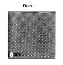
Figure 1 provides an AC mode AFM image of silver features obtained by
deposition
of 10 wt % Ag in a commercial nanoparticle ink in tetradecane diluted 7:2:1
heptadecane:a-
terpineol:octanol at 20.8 C and 49.6 % humidity using a A-frame cantilever
with spring
constant 0.1 N/m.
Figure 2 provides an AC mode image of SiO2 surface showing 300 nrn features
spaced by 5 m obtained by depositing 20 wt % Ag in a commercial nanoparticle
ink in
water diluted by glycerol. Deposition was performed at 23.8 C and 31.2 %
relative humidity
using a diving-board cantilever with a spring constant 0.5 N/m.
Figure 3 provides an AC mode AFM image showing a continuous Ag line obtained
by
spotting the water-glycerol-based ink as in Figure 2 with a 200 nm pitch. The
line is 800 nm
wide and 5 nm tall. Deposition was performed at 22.5 C and 50.2 % humidity
using an A-
frame cantilever with spring constant 0.5 N/m.
Figure 4 provides an image and table showing the dependence of feature size on
amount of water-glycerol-based ink deposited. The first spot on the left has
the highest
volume of ink deposited, and is therefore the widest and tallest feature. The
third spot on
3
CA 02701889 2010-04-07
WO 2009/052120 PCT/US2008/079893
right has least amount of deposited ink. Deposition was performed at 23.3 C
and 50.9 %
humidity using a diving-board tip with spring constant 0.5 N/m.
Figures 5A, 5B, and 5C provide optical images of (A) a universal inkwell, (B)
cantilever dipping into Inkwell, and (C) good ink spreading and loading on a A-
frame
cantilever (spring constant 0.1 N/m), respectively. The ink comprises wt.% Ag
in 7:2:1
heptadecane:alpha-terpineol:octanol ink.
Figures 6A provides an Optical microscopy image of bleeding excess silver
nanoparticle (AgNP) ink with both cantilever and tip of a contact mode tip; 6B
shows an
AFM topography scanning image of tip bleeding dots; and 6C shows the cross-
sectional
topography trace of a line (marked by the dot line in 6B through the three
dots.
Figures 7A-7B provide a schematic representation of the procedure used to
direct-
print AgNP inks on a SiO2 substrate, including (i) inking the tip and (ii)
depositing the ink.
Figure 8 provides a table of comparison of the results for three different
AgNP ink
systems used in one experiment.
Figures 9(i) provides an AFM topography image of silver dots generated via
increasing tip-substrate contact times (A-F in Figures 9(i)). The
identification letter, time of
ink printing, and measured diameter of the dots are as follows: A: 0.1 s,
1.972 m; B: 0.2 s,
2.828 m; C: 0.5 s, 3.87 m; D: 1 s, 4.466 m; E: 2 s, 4.947 m; F: 5 s,
5.603 m; 9(ii)
shows the cross-sectional topography trace of a line (marked by the dot line
in (i)) through
the three dots. 9(iii) shows curves of the average silver dot diameter plotted
as a function of
dwell time for an AgNP and MHA inks.
Figures IOA shows an AFM topography image of five silver lines generated via a
scan rate of 10jJs and l OB shows the cross-sectional topography trace of a
line (marked by
the white line in (a)) through the five lines.
Figures 11 A-11 E provide characterization of some silver lines generated. 11
A
provides an optical image showing continuous silver lines; 11 B-11 C show a
silver line SEM
images under different magnifications; I ID provides results of conductivity
measurements
after different annealing temperatures; and 11 E provides the results of
conductivity
measurement after annealing at 200 T.
DETAILED DESCRIPTION
INTRODUCTION
All references cited herein are hereby incorporated by reference in their
entirety.
4
CA 02701889 2010-04-07
WO 2009/052120 PCT/US2008/079893
For deposition and direct write lithography processes, including use of AFM
probe to
deposit structures on solid surfaces, see for example Ginger et al., Angew.
Chem. Int. Ed.
2004, 43, 30-45. See also, Salaita et al., Nature Nanotechnology 2, 145 - 155
(2007).
Direct write processes are described in for example Direct-Write Technologies
for
Rapid Prototyping Applications, Sensors, Electronics, and Integrated Power
Sources, (Ed.
Pique, Chrisey), 2002, including Chapter 7 (ink jet methods), Chapter 8
(micropen methods),
Chapter 9 (thermal spraying), Chapter 10 (Dip-Pen Nanolithography), Chapter 11
(Electron
beam), and the like. Chapter 18 describes pattern and material transfer
methods.
US Patent Nos. 6,635,311; 6,827,979; 7,102,656; 7,223,438; and 7,273,636 to
Mirkin
et al. describe various materials and methods which can be used as needed in
practicing the
embodiments described herein.
US Patent Publication No. 2005/0235869 to Cruchon-Dupeyrat describes more
materials and methods which can be used as needed in practicing the
embodiments described
herein, including measuring the resistivity of metallic lines.
INK COMPOSITION
Ink compositions can be formulated for use in loading onto a deposition
instrument,
and for subsequent use in the deposition instrument in deposition onto a
substrate surface.
For example, viscosity and stability can be formulated. The composition can
comprise
metallic nanoparticles and a carrier system. The composition can be non-
reactive at 25 C and
atmospheric pressure in air. In particular, the composition can be sol-gel non-
reactive at
25 C and atmospheric pressure in air. Sol gel compositions are known in the
art. See for
example Sol-Gel Science, The Physics and Chemistry of Sol-Gel Processing,
Brinker,
Scherer, 1990. The composition can comprise one or more additional components
such as
additives such as for example stabilizers and surfactants.
The ink can be a water based ink or an organic based ink. For example, the ink
can
comprise water, an organic solvent, a plurality of nanoparticles and
combinations thereof.
Other writeable inks can be used, including those comprising for example
alkanethiols, sol-
gel, antibody/antigen, lipid, deoxyribonucleic acid (DNA), block copolymer,
and inorganic
nanoparticles.
NANOPARTICLES
Nanoparticles and metallic nanoparticles are generally known in the art. For
example,
nanoparticles are described in US Patent Publication No. 2005/0235869 to
Cruchon-
Dupeyrat, and references cited therein. Nanoparticles can have an average
diameter of for
example about 1,000 nm or less, or about 500 nm or less, or about 250 nm or
less, or about
CA 02701889 2010-04-07
WO 2009/052120 PCT/US2008/079893
100 nm or less. The minimum average diameter can be for example about 1 nm, or
about 3
nm. The nanoparticles can be of a size that their melting point is reduced
compared to a
corresponding bulk material. Nanoparticles can have for example an average
particle size of
1 nm to 25 nm, or about 1 nm to about 10 nm. The size can be sufficiently
small so that
melting point is reduced to allow lower temperature sintering of particles
into a coherent film.
In many cases, the goal is to provide a nanoparticle system which will enable
production of a
high electronic conductivity material on a substrate.
Nanoparticles can be metallic nanoparticles including for example transition
metal
particles such as for example titanium, tantalum, niobium, iron, copper,
ruthenium,
molybdenum, nickel, cobalt, platinum, palladium, gold, or silver
nanoparticles, or
combinations of these metals or their alloys. In particular, conductive
materials such as
copper, gold, and silver can be used. The metal can be in a zero valent state.
It can form
conductive materials upon consolidation of individual nanoparticles into a
coherent film.
Nanoparticles can have a uniform structure. For example, the nanoparticle can
contain one material or element in the particle. Nanoparticles can have a core
shell structure.
The nanoparticle can contain one material or element in the core and one
material or element
in the shell. The nanoparticles can be capped nanoparticles or uncapped
nanoparticles. The
nanoparticles can be charged or neutral nanoparticles.
Nanoparticles can have an average particle size of, for example, about 1 nm to
about
100 nm, or about 1 nm to about 50 nm, or about 5 nm to about 50 nm, or about 3
nm to about
25 nm. The particle size distribution can be polydisperse or substantially
monodisperse.
Nanoparticles can comprise metal alloys.
Nanoparticles can be nanocrystals. See for example, The Chemistry of
Nanostructured Materials, (Ed. P. Yang), including the chapter on
nanocrystals, pages 127-
146. Nanoparticles are also described in Watanabe et al., Thin Solid Films,
435, 1-2, July 1,
2003 (pages 27-32).
The nanoparticles can be adapted to provide stability using for example
stabilizers and
surfactants.
The nanoparticles can be magnetic nanoparticles.
Nanoparticles can be obtained from commercial suppliers. See for example
Harima
Chemicals (Tokyo, Japan) including NP series, and PChem Associates (Bensalem,
PA)
including a PF1200 product and a PFi-201 Silver Flexographic ink.
AQUEOUS-BASED CARRIER SOLVENT SYSTEM
6
CA 02701889 2010-04-07
WO 2009/052120 PCT/US2008/079893
The aqueous based carrier system can be adapted for direct writing including
direct
writing with use of a cantilever, with a scanning probe microscope tip, and/or
an atomic force
microscope tip. The tip can be hollow or non-hollow.
The carrier system or solvent system can comprise water, at least one organic
solvent
miscible in water, or a combination thereof. In one embodiment, the carrier
system
comprises water and at least one organic solvent immiscible in water. The
organic solvent
can be a liquid at 25 C and atmospheric pressure. The organic solvent miscible
in water can
be a polar solvent including for example an oxygen-containing solvent.
The carrier system or solvent system can comprise at least one solvent, or at
least two
solvents, or at least three solvents.
Examples of organic solvent include glycerol, ethylene glycol, poly(ethylene
glycol),
Tween 20 (polysorbate surfactant), and the like. The organic solvent can be
for example a
polyol such as for example a compound comprising at least two, or at least
three hydroxyl
groups such as for example, glycerol.
The organic solvent can have a molecular weight of about 300 g/mol or less, or
about
200 g/mol or less, or about 100 g/mol or less.
The organic solvent can have a boiling point at 760 mm Hg, for example, of
about
200 C to about 350 C, or about 250 C to about 300 C. The melting point can be
less than
about 20 C. The boiling point can be similar to glycerol which is about 290 C
at 760 mm Hg.
The organic solvent can have a viscosity at 25 C which is greater than the
viscosity of
water at that temperature but less than three times, or less than two times
the viscosity of
glycerol at that temperature. The organic solvent can have a viscosity similar
to that of
glycerol. For example, the viscosity of glycerol is about 934 mPa-s at 25 C.
Hence, the
viscosity of the organic solvent can be for example about 2 mPa-s to about
2,000 mPa-s at
25 C, or about 100 mPa-s to about 1,500 mPa-s at 25 C.
If desired, the composition can further comprise one or more additives. For
example,
surfactants or dispersants can be used in the formulation to help stabilize
the nanoparticles.
Stabilizers or dispersants can be used.
The solvent carrier can be adapted so that viscosity is sufficient to allow
the ink
composition to wet a cantilever or a tip of a cantilever and provide a uniform
coating thereon.
One skilled in the art can adapt the carrier system to provide the best
stability or shelf
life for the ink formulation.
The pH can be adapted as needed for best application.
Surfactants can be used to tune the contact angle.
7
CA 02701889 2010-04-07
WO 2009/052120 PCT/US2008/079893
The nanoparticles and the solvent system can be combined by sonication or aqua-
sonication by a vortex system. Well-suspended nanoparticles in a solvent
system can be
relatively opaque, in contrast to a relatively transparent system with
nanoparticles not well-
suspended in a carrier.
AMOUNTS
The amounts of the components in the ink formulation can be measured by weight
percentage. For example, the amount of metallic nanoparticle can be for
example about 5
wt.% to about 35 wt.%, or about 10 wt.% to about 35 wt.%, or about 15 wt.% to
about 25
wt. %.
The amount or concentration of the nanoparticles can be adapted to control the
size of
the deposit and the amount of material deposited.
The weight ratio of water to organic solvent can be for example about 4:1 to
about
1:4, or about 3:1 to about 1:3, or about 2:1 to about 1:2, respectively.
The weight percentage of water can be greater than the weight percentage of
organic
solvent. Or, the weight percentage of organic solvent can be greater than the
weight
percentage of water.
One skilled in the art can adapt the amounts so that suitable viscosity can be
achieved
to adequate coat a cantilever with nanoparticles for subsequent deposition.
LOADING INK FOR DEPOSITION
The ink composition can be subjected to an immersion step where material is
transferred to for example a cantilever or a cantilever comprising a tip. For
example, US
Patent No. 7,034,854 describes ink delivery methods. See also commercial ink
well products
available from Nanolnk (Skokie, IL) including universal inkwells (see Figures
5A and 5B).
For example, ink can be loaded into reservoirs, and can be transferred down
channels to wells
which are adapted for dipping a tip or a cantilever into the well.
Microfluidics can be used
for ink transport. See for example Microfluidic Technology and Applications,
Koch et al.,
2000.
The ink composition can be used wet after transfer. Attempt to encourage
drying can
be avoided so that any drying which occurs is only from natural drying. In
some cases,
drying steps can be used but then it may be desirable to use wet conditions
for transfer of the
ink to the substrate (e.g., high humidity values).
The ink composition can also be transported to an end of a tip as known in the
art.
The hollow or open tip can be adapted to avoid clogging.
SUBSTRATE
8
CA 02701889 2010-04-07
WO 2009/052120 PCT/US2008/079893
The substrate and substrate surface can be a variety of solid surfaces
including for
example semiconductor surface, conductive surface, insulating surface, metal
surface,
ceramic surface, glass surface, polymeric surface, and the like. The surface
can be organic or
inorganic. The surface can be charged or neutral. The surface can be surface
modified to
make it more hydrophilic (for example, piranha treatment) or more hydrophobic
(for
example, HF treatment).
The substrate can have a surface which is modified by an organic layer based
on for
example self assembled monolayers (SAMs), including surface molecules
presenting
different functionalities such as carboxylic acid, and also use of at least
one silane, thiol,
phosphate, and the like. For example, MHA modified surfaces can be used.
The substrate surface can be silicon or silicon dioxide. Substrates can
comprise heat
stable polymer such as, for example, polyimide.
The substrate surface can be one useful in printed electronics or the
semiconductor
industry.
The substrate does not need to react with or chemically bind to the metallic
nanoparticles.
The temperature of the substrate surface can be varied as needed such as
heated to
improve deposition including for example heating on a hot plate or in an oven.
Substrates can be cleaned as needed.
DEPOSITION
Deposition can be carried out with for example an NSCRIPTOR instrument
available
from NanoInk (Skokie, IL). Alignment software can be used such as for example
INKCAD.
See also alignment in US Patent No. 7,279,046 and calibration in US Patent No.
7,060,977.
Deposition can be also carried out with an SPM instrument including an AFM
instrument.
See also US Patent Nos. 6,635,311; 6,827,979; 7,102,656; 7,223,438; and
7,273,636 to
Mirkin et al. See also US Patent Publication No. 2005/0235869 to Cruchon-
Dupeyrat.
Additional Nanolnk patents include, for example, 7,005,378; 7,034,854;
7,098,056;
7,102,656; and 7,199,305.
Nanolnk provides commercial products including for example 2D nanoprintarrays,
active pens, AFM probes, bias control option, chip cracker kit, inkwells,
InkCAD, vacuum
pucks, and sample substrates.
Other instruments are described in for example US Patent No. 7,008,769 and US
patent publication no. 2005/0266149 to Henderson et al. See also US Patent No.
6,573,369.
9
CA 02701889 2010-04-07
WO 2009/052120 PCT/US2008/079893
Scanning probe microscopy and surface modifications with same are described
in, for
example, Bottomley, Anal. Chem., 1998, 70, 425R-475R; and Nyffenegger et al.,
Chem. Rev.,
97, 1195-1230.
Feedback mode can be used. No-feedback mode can be used.
In many cases, constant height mode can be used rather than constant force
mode.
In some embodiments, prior to the deposition, "bleeding" can be used. Bleeding
in
some cases can refer to holding the cantilever and/or tip very close to the
surface of the
substrate and subsequently withdrawing the cantilever and/or tip from the
surface to remove
excess ink from the cantilever and/or tip onto the substrate.
During deposition, the cantilever can be moved over the surface or held
constant over
the surface.
The deposition can be carried out at temperatures of for example about 20 C to
about
35 C.
The cantilever can have a variety of spring constants which can be adapted for
a
particular application.
The cantilever can comprise a tip at the end. Alternatively, the cantilever
can
comprise no tip at the end, and can be for example a tipless cantilever. The
cantilever tip can
be cleaned as needed but can comprise a hard material such as silicon nitride
without coating.
The tip can comprise an SPM tip, an AFM tip, a nanoscopic tip, and can be
solid or hollow.
Deposition can be carried out at sufficiently high humidity to encourage
deposition.
For example, relative humidity can be at least 30%, or at least 50%.
Deposition can be carried out on the same place multiple times to build up
height.
Multi-layer structures can be formed. These can comprise for example at least
two, or at least
three, or at least five, or at least ten layers. In some cases, the height and
the lateral
dimensions such as length or width can be increased by use of multiple
depositions on the
same spot. However, the aspect ratio of height to lateral dimension can stay
substantially the
same despite multiple depositions, which can be an advantage. For example,
aspect ratio can
be between about 10 and about 40, or between about 20 and about 30, for
example. See
Working Example 4 and Figure 4. A controlled aspect ratio with multiple
spotting can be
indicative of a controlled system.
Parallel and massively parallel probe systems can be used for increased rates
of
deposition.
Thermal DPN printing can be used.
CA 02701889 2010-04-07
WO 2009/052120 PCT/US2008/079893
Electrostatic and thermal or piezoelectric actuation of probes and cantilevers
can be
used.
TREATMENT AFTER DEPOSITION
The structures disposed or deposited on the substrate can be treated with
heat. Heat
treatment is sometimes referred to as "annealing" or "curing." Heat can be
applied via
external methods such as an oven or exposure to light beam. The heat treatment
can be
adapted for both time and temperature and can be adapted to provide for
sintering of
nanoparticles to form a continuous film and also removal of solvent carrier as
well as
organics as appropriate. Heat treatment can be executed at for example about
100 C to about
1,000 C, or about 200 C to about 600 C, or about 300 C to about 500 C. In many
cases,
conditions will be adapted to achieve high conductivity and compatibility with
substrate and
other components in the system.
The curing time can be varied from for example two seconds to three hours, or
two
minutes to two hours.
In some cases, it is desired that the deposited droplet will shrink as it
dries allowing
for smaller structures.
DEPOSITED STRUCTURES
The structures disposed on the substrate can be continuous or discontinuous
although
in general the ultimate goal is to make a conductive continuous structure. For
example, the
structures can be lines or dots or spots.
If dots are spaced close enough to overlap, continuous structures including
lines can
be generated. The pitch between structures can be varied and can be for
example less than
about 1,000 nm, or less than about 500 nm, or less than about 200 nm. Ordered
arrays can be
fabricated. Pitch can be measured as edge-to-edge distance or from a center
point of a
structure such as a center of a circle or the middle of a line.
In one embodiment, the structures are continuous and have a substantially
uniform
height. For example, a dot can have a substantially uniform height, or a line
can have a
substantially uniform height.
The thickness or height, the length, and the width can be adapted for a
particular
application. In many cases, it is desirable to have at least one lateral
dimension which is for
example about 1,000 nm or less, or for example about 1 nm to about 5,000 nm,
or about 10
nm to about 1,000 nm, or about 25 nm to about 500 nm. One embodiment has a
lateral
dimension of about 1,000 nm to about 5,000 nm.
11
CA 02701889 2010-04-07
WO 2009/052120 PCT/US2008/079893
The rate of the deposition or dwell time can be used to adjust size. In
addition,
multiple depositions can be carried out as desired on the same spot to adjust
height and/or a
lateral dimension.
A lateral dimension can be for example a substantially circular diameter or a
line
width.
The height or thickness can be, for example, about 1 nm to about 50 nm, or
about I
nm to about 10 nm, or about 3 nm to about 8 nm.
An important advantage is to build up height to a distance appropriate for the
application.
CHARACTERIZATION
The structures disposed on the substrate can be characterized by methods known
in
the art including for example scanning probe microscopy including AFM.
Electrical conductivity or resistivity can be measured by methods known in the
art.
Resistivity can be adapted with use of different thicknesses and widths of the
conductive line.
OTHER DEPOSITION METHODS
The compositions and inks described herein can be applied to surfaces by other
methods including for example direct write methods, soft lithography methods,
including for
example microcontact printing and ink jet printing. Soft lithography and
microcontact
printing are described in for example Xia et al., Angew. Chem. Int. Ed. 1998,
37, 550-575.
Ink jet printing and other direct write methods are described in for example
Direct- Write
Technologies for Rapid Prototyping Applications, Sensors, Electronics, and
Integrated
Power Sources, (Ed. Pique, Chrisey), 2002, including Chapter 7 (ink jet
methods), Chapter 8
(micropen methods), Chapter 9 (thermal spraying), Chapter 10 (Dip-Pen
Nanolithography),
Chapter 11 (Electron beam), and the like. Chapter 18 describes pattern and
material transfer
methods.
Another deposition method is described in Kraus et al., Nature Nanotechnology,
2,
570-576 (2007). In this method, the authors developed a printing process that
enables
positioning of sub-100-nm particles individually with high placement accuracy.
A colloidal
suspension was inked directly onto printing plates, whose wetting properties
and geometry
ensure that the nanoparticles only fill predefined topographical features. The
dry particle
assembly was subsequently printed from the plate onto plain substrates through
tailored
adhesion. The authors demonstrated that the process can create a variety of
particle
arrangements including lines, arrays and bitmaps, while preserving the
catalytic and optical
activity of the individual nanoparticles.
12
CA 02701889 2010-04-07
WO 2009/052120 PCT/US2008/079893
ORGANIC-BASED CARRIER SOLVENT SYSTEM
In another embodiment, the carrier solvent system can comprise a terpene
alcohol
such as a monoterpene alcohol such as a such as for example alpha-terpineol.
For example, a first component (A) of the solvent carrier system can be a high
boiling
hydrocarbon such as for example a long chain alkane like tetradecane,
pentadecane,
hexadecane, or heptadecane, or combinations thereof.
A second component (B) of the solvent carrier system can be a terpene alcohol
such
as for example a monoterpene alcohol such as alpha-terpineol.
A third component (C) of the solvent carrier system can be an alkanol such as
for
example a long chain alkanol such as octanol or decanol.
A mixture in wt. ratios of A, B, and C can be formulated at 7:2:1 and used to
dilute a
stock solution of nanoparticles.
In this embodiment, the weight percentage of metallic nanoparticles can be for
example about 5 wt.% to about 20 wt.%.
APPLICATIONS
The compositions and methods described herein can be used in a variety of
applications including, for example, applications cited in references cited
herein including for
example thin film transistor (TFT) fabrication, circuit editing, photomask
repair, photonic
crystals, chemical-/bio-sensors, waveguides, and generally applications which
include use of
a metal line or a conductive metal or an electrode.
Photomask repair applications are described in for example US Patent
Publication
Nos. 2004/0175631 and 2005/0255237.
Conductive lines and applications thereof are described in for example US
Patent
Publication No. 2005/0235869.
Other applications include MEMS and NEMS related applications.
Applications with conductive structures are also described in for example
Fundamentals of Microfabrication, The Science of Miniaturization, 2d Ed., M.
Jadou, 2002,
including Chapter 10. Transistors are described in for example Thin-Film
Transistors,
(Kagan, Andry, Eds), 2003.
Conductive electrodes can be also important in solar cell applications. See
for
example, Organic Photovoltaics, Mechanisms, Materials, and Devices, (Eds. Sun
and
Sariciftci), 2005. Electrodes are also used in OLED, PLED, and SMOLED
technologies.
Other applications include for example catalysts, fuel cells, food
preservation, and
drug delivery.
13
CA 02701889 2010-04-07
WO 2009/052120 PCT/US2008/079893
Nanoparticles can be also used in bio-oriented applications. See for example
Nanobiotechnology II, More Concepts and Applications, (Ed. Mirkin and
Niemeyer), 2007,
and discussions of nanoparticles in chapters 3, 6, and 7 for example.
NON-LIMITING WORKING EXAMPLES
A series of non-limiting working examples are provided to further illustrate
various
embodiments.
EXAMPLE 1:
Materials and Methods:
Experiments were performed with Nanolnk's NSCRIPTOR system, operating on
vibration isolation air-table and in an environmental chamber. Chemicals used
(glycerol,
heptadecane, hexadecane, pentadecane, a-terpineol, octanol and decanol) were
purchased
from Sigma Aldrich and used without further purification. A 70 wt % silver
nanopaste (5 nm
particles in tetradecane) was purchased from Harima Chemicals (Japan), and
stored in a
refrigerator until use. A 40 wt % silver nanoparticle (15 nm particles)
solution in aqueous
solvents (water, surfactants, and adhesives) was purchased from PChern
Associates (PFi-201
Silver Flexographic Ink). Inks with varying ratios of solvents were formulated
by pippetting
known amounts of liquid into a clean glass vial. A mass balance was used to
accurately add
silver nanoparticles until the ink had the desired weight percent.
A-type cantilevers (spring constant 0.1 N/m) and M-type cantilevers (spring
constant
0.5 N/m) were 02 plasma cleaned before use. Cantilevers with varying spring
constants were
coated with ink by dipping the cantilevers in microfluidic based inkwells for
about 2 seconds.
Ink was then deposited onto substrates when the cantilever was brought into
contact with the
surface, either in constant force mode or in constant height mode. The amount
of time the
cantilever was in contact with the surface (dwell time) was controlled by
InkCAD software.
Patterning was achieved using liquid inks. Sometimes excess ink was bled off
from
the cantilever before patterning.
Figure 5C illustrates good ink spreading onto the cantilever to provide a
uniform film
which is important for uniform patterning.
EXAMPLE 1(a): ORGANIC CARRIER SYSTEM
One organic ink was based on 10 wt % silver nanoparticles in 7:2:1
heptadecane:a-
terpineol:octanol.
The ink was produced by first diluting a highly viscous Ag nanoparticle stock
solution
with a diluting solution comprising a combination of solvents. The combination
of solvent
14
CA 02701889 2010-04-07
WO 2009/052120 PCT/US2008/079893
was varied to determine best composition of the solvents. The diluted Ag
nanoparticle
solution was then deposited by a cantilever onto the substrate
lithographically in a spotting
manner. The substrate with the deposited Ag inks were then annealed to obtain
continuous
features.
For the organic ink, the Ag particles 70 wt % silver nanoparticles (5 nm in
diameter)
in tetradecane purchased from Harima Chemicals, Japan was used. Investigations
were
performed to obtain a dilution solution with an appropriate solvent
combination that was
liquid at room temperature, spread on the cantilever uniformly, did not
rapidly evaporate, and
was miscible with tetradecane. Examples of these solvents were long chain
alkanes
(pentadecane to heptadecane), alcohols (octanol and decanol) and a-terpineol.
An
embodiment was developed for a 10 wt % silver nanoparticles in 7:2:1
heptadecane:a-
terpineol:octanol ink for reproducible deposition of silver nanoparticles. It
was found that
varying the concentration of silver nanoparticles between 5 and 20 wt % did
not appreciably
change the properties of the ink. While different ratios of solvents were
used, the 7:2:1
worked the best.
After inking the cantilever, the ink was deposited onto a silica (Si02)
substrate in a
spotting manner using a dwell time of 0.01 s per spot. About 10 such arrays
were written
before running out of ink on the cantilever. The substrate was then annealed
on a hot plate to
about 400 C for 30 minutes. Figure 1 shows a dot array obtained after
annealing the
substrate following deposition with the 10 wt % Ag in 7:2:1 heptadecane:a-
terpineol:octanol
ink. The features are between 1.7 - 2.2 m in diameter and 4 - 7 nm in height.
Similar
features were obtained by using different solvents from the same family, such
as hexadecane
being substituted for heptadecane or decanol being used instead of octanol.
Larger features
were obtained by increasing the dwell time, thereby allowing more ink to flow
from the
cantilever to the substrate. Finally, continuous features were obtained,
thereby substantially
eliminating the "coffee ring" effects and the non-continuous features produced
by ink jet
printing and DPN printing because during the anneal process, the evaporating
solvent carries
the nanoparticles towards the center of the spot. This is in stark contrast to
"coffee ring"
effects, or not continuous features obtained by ink jet printing and DPN
experiments.
EXAMPLE 1(b): SURFACE HYDROPHILICITY/HYDROPHOBICITY
To obtain features with nanoscale diameters with this ink, the effect of
surface
chemistry was investigated. Two surfaces, one hydrophobic, one hydrophilic
were prepared
by immersing the substrates in hydrogen fluoride (HF) and piranha,
respectively, for the ink
CA 02701889 2010-04-07
WO 2009/052120 PCT/US2008/079893
to bead up on the hydrophilic surface, and to spread readily on the
hydrophobic surface.
Beading up of the ink can reduce the size of the footprint of the ink on the
surface, resulting
in smaller features. However, features obtained on the hydrophilic surface had
some
dimensions still in the micron regime, though they were about 26 nm tall.
Thus, these results
suggest that the determining factor in the size of the feature in this
embodiment was
controlled by the droplet of ink coming off the cantilever, and not be
variations in surface
chemistry, or dwell times. Therefore, to obtain features with nanoscale
diameters, the size of
the droplet at the end of the cantilever can be changed.
One method to accomplish this goal is to change the surface tension of the
ink.
Surface tension is an interfacial phenomenon that tends to minimize the
exposed surface area
of the liquid. Aqueous solvents have hydrogen bonding interactions between
individual
molecules, which are stronger than van der walls interactions present between
molecules of
the hydrophobic ink. Thus, although the present inventions are not limited by
theory,
aqueous based inks may form smaller droplets of ink as the ink is being
deposited on the
surface.
EXAMPLE 1(c): AQUEOUS INK CARRIERS
For the aqueous ink, 15 nm silver nanoparticles (40 wt %) in aqueous
surfactant were
purchased from PChem Associates, Inc. In the investigation of obtaining a good
combination
of solvent for the dilution solution, it was found that among the solvents,
such as poly
(ethylene glycol), Tween 20 (polysorbate surfactant), ethylene glycol, and
glycerol, except
glycerol, the nanoparticles aggregated within 1 hour, whereas in glycerol they
remained
suspended for about 5 hours. Additionally, the nanoparticles can easily be re-
suspended in
glycerol by sonicating the ink for 2 minutes followed by placing the ink vial
on a vortex for
30 seconds. This ink can have a very long shelf-life, and can potentially be
used indefinitely.
In one experiment performed to determine the hold time of the glycerol
solvated Ag
nanoparticle ink on the cantilever, the ink was formulated in a 1:1 ratio of
the stock silver
nanoparticle surfactant solution to glycerol, resulting in a 20 wt % silver
nanoparticle ink.
The results from optical observations showed that from a small amount (0.2 L)
of the ink, it
took over 20 minutes for the ink to evaporate from the cantilever.
The aqueous ink (20 wt % Ag NP in 1:1 glycerol: surfactant) was spotted on a
Si02
substrate with a dwell time of 0.01 s. Figure 2 illustrates that after
annealing the substrate at
500 C for 30 minutes, continuous dots that were about 300 nm in diameter and
about 5 nm
tall were obtained. Additionally, by spotting the ink with a 200 nm pitch,
continuous lines
16
CA 02701889 2010-04-07
WO 2009/052120 PCT/US2008/079893
was obtained with this ink because the nanoparticles sintered together during
the anneal
process; see Figure 3. Continuous features were obtained because during
evaporation, the
solvent formed a meniscus, which carrier the nanoparticles towards the center
of the spot.
Similar results were obtained by using inks that had a higher concentration of
silver
nanoparticles, or by using inks that are suspended in solvents similar to
glycerol, or using
different concentrations of glycerol.
EXAMPLE 1(d): SPOTTING IN SAME LOCATION
In one embodiment, for both organic and aqueous inks, the sizes (both width
and
height) of the features depended on the amount of ink deposited, which in turn
can be
controlled by the number of times the ink was spotted in the same location.
Figure 4
demonstrate this dependence of the aqueous ink on a sample. The dwell time was
10 mS. It
was observed that the deposition from 10 repetitions of spotting resulted in
the widest and
tallest features in the group.
For both the organic and aqueous inks, the Alignment feature of InkCAD was
used to
return to the previously written features for imaging after annealing.
EXAMPLE 2:
In this series of experiment, Nanoink's inkwell, single pen tip, and plasma
enhanced
chemical vapor deposition (PECVD) Si02 substrate were oxygen plasma cleaned
for 3 min
with a moderate power at 300 torr to remove organic contamination and create a
fresh
surface. A hydrophilic drop-on-demand (DOD) inkjet silver nanoparticle (AgNP)
ink, which
was a water based ink (PFI200, PChem Associate), was used. The ink was loaded
to the
microfluidic channel of inkwell chip, and to load the ink on the tip and
cantilever, the scanner
was aligned and further lowered down such that the ink in the microchannel
wetted the tips
and partially the cantilever surface due to surface tension. See Bjoern et
al., Smart Materials
& Structures 15 (1): 5124-30 (2006); Rivas-Cardona et al., Journal of
Microlithography,
microfabrication, and Microsystems 6(3) (2007).
Figure 6A shows a standard contact mode silicon nitride (SiN) tip after ink
loading on
triangular cantilever and the following wetting traces of excess AgNP ink,
herein referred to
as "bleeding," on silicon dioxide substrate with both cantilever and tip by
bringing inked tip
in contact with substrate. After curing by a 200 C hotplate for 10 min, the
traces were
scanned by an AFM in the AC mode with a scan rate of 1 Hz. The AFM topography
image
and the trace cross section through the bleeding dots are shown individually
in Figures 6B-
6C. The diameter of the tip bleeding dot was about 10 m, with an average
height of about
25 nm, which was doubly larger than the size of the tip pyramid base (5 m).
At this stage, a
17
CA 02701889 2010-04-07
WO 2009/052120 PCT/US2008/079893
continuous tip bleeding was used to remove the over-rich ink such that a
moderate ink
coating on tip can be obtained. This can be determined optically by the
reduced size of tip
bleeding dot down to about 2 gm or even smaller.
In comparison to conventional mercaptohexanoic acid (MHA) DPN process, which
utilize native water meniscus in a humid environment to transport MHA, the
liquid phase
DPN process was carried by surface tension behavior. A schematic of liquid
phase DPN
process for DOD inkjet AgNP ink is illustrated in Figure 7. A cleaned Si02 or
SiN surface is
more hydrophobic than the ink, and the hydrophilic ink can be transferred from
the SiN tip to
the Si02 substrate because the ink has low affinity to either surface.
The ability to manipulate the hydrophilicity was verified by contrasting a
water-based
ink as described above with an organic based ink (NST05, NanoMas Technologies,
Inc.).
The results show that after inking the surface of the cantilever, ink
transportation from the tip
to the substrate during bleeding did not occur. Additionally, the solvent
dried up such that
the DPN of organic AgNP did not occur. Comparisons of the DPN results of three
different
inks are provided in Figure 8. A comparison of contact angle by different inks
onto a oxygen
cleaned substrate was also performed to simulate a writing condition.
An organic hydrophobic ink from InkTec (InkTec, Irvine, CA) was also tested.
It
was observed that the ink was very hydrophobic, and the DPN can only be
performed on a
hydrophobic surface, such as the Inkwell substrate surface.
Additionally, ethylene glycerol/hydrophilic based nano silver particle inks
(NovaCentrix Inc., Texas) were also tested. The results show that the inks
with 10% Ag and
40% Ag were direct "DPN-able," but never the less exhibit issues with respect
to fast drying,
viscosity, and hydropolarity. Further, it was found that with these inks
uniform dot/line
writing was more difficult to obain.
The results demonstrated a water based ink with a slow dry-rate and a proper
viscosity
can facilitate the DPN process.
To minimizing the problem of ink drying too fast, a solvent with a high
boiling point
temperature was added. In one embodiment, the solvent was hydrophilic glycerol
(boiling
point is 182 C at 20 mmHg) in a AgNP ink. Note that other solvent may be
added, including
octanonl, dodecane, or PEG. It was observed that a drop of this modified ink
in Inkwell can
remain over 2 weeks. Additionally, the AgNP were stabilized and well-suspended
in the
solvent through a layer coating of functional surfactant; see Bao et al., I
Mater. Chem 17,
p1725 (2007). To retract the homogeneous particle suspension after adding
glycerol, about
min of vortexing in Vortexer (Southwest Scientific), followed by 20 min of
ultrasonication
18
CA 02701889 2010-04-07
WO 2009/052120 PCT/US2008/079893
was used to obtain an opaque black ink. Furthermore, the DPN process was
performed
under a constant height mode without aligning laser spot on the cantilever to
avoid heating
the cantilever and to facilitate evaporation of the solvent.
The dot calibration with different dwell times was performed and the AFM
topography, cross-section, and the average silver dot diameter curves plotted
as a function of
dwell time are shown in Figures 9A-9C. A trend of increasing dot size with
increasing dwell
time is shown in Figures 9A-B. The dot calibration for AgNP was also compared
with
another common DPN inks, MHA, as shown in Figure 9C. not to be bound by any
particular
theory, the fitted curves in Figure 9C provides the intersection in y-axis
that show the initial
ink loading on the tip, and the maximum dot indicate the ink morphology
between top-
substrate reach an equilibrium. Further, not to be bound by any particular
theory, the DPN
process with MBA ink can be dominated by chemi-sorption, whereas that with
AgNP ink can
be dominated by physi-sorption because there is substantially no specific
chemical binding
between solvent and Si02 surface, or AgNP and Si02 surface. Thus, surface
tension affected
the feature size and the system was a physic-sorption process in this
embodiment.
To evaluate the future applications, 40 m lines with chosen writing speed
were
demonstrated. Figures 1OA-10B show both the AFM topography and the cross-
section height
profile, respectively. The minimum width was about 760 nm, and for line width
greater than
2 m (see Figures 11 A-11 C), conductivity measurements were conducted; the
results are
shown in Figures 11C-D. As seen in the optical image of the lines in Figure
11A, the lines
are continuous.
The lines with contact metal as-deposited show minimal conductivity, acting
similarly
to an electrical insulator (see Figure 11D). However, after the lines were
annealed at 200 C,
they began to exhibit conducting behavior (see Figures 11D-11E). Not to be
bound by any
particular theory, the high electrical resistance can arise from the very thin
layer of AgNP
(about 20-30 nm) and/or possible surface oxidation, and the conducting
behavior may be
attributed to the removal of the Schottky defects in the silver metal lines by
annealing.
One skilled in the art can employ the following references in carrying out
claimed
embodiments:
1. Daniel Huang, Frank Liao, Steven Molesa, David Redinger, and Vivek
Subramanian,
"Plastic-Compatible Low Resistance Printable Gold Nanoparticle Conductors for
Flexible
Electronics," J. Electrochem. Soc., Volume 150(7), pp. G412-G417 (2003).
19
CA 02701889 2010-04-07
WO 2009/052120 PCT/US2008/079893
2. Seamus E. Burns, Paul Cain, John Mills, Jizheng Wang, and Henning
Sirringhaus, "Inkjet
printing of polymer thin-film transistor circuits," MRS bulletin 28 (11),
pg:829 -834
(2003).
3. Seung H Ko, Heng Pan, Costas P. Grigoropoulos, Christine K. Luscombe, Jean
M J
Frechet, and Dimos Poulikakos, "All-inkjet-printed flexible electronics
fabrication on a
polymer substrate by low-temperature high-resolution selective laser sintering
of metal
nanoparticles," Nanotechnology 18, 345202 (2007).
4. Venugopal Santhanam and Ronald P. Andres, "Microcontact Printing of Uniform
Nanoparticle Arrays," Nano Letters 4 (1), 41-44 (2004).
5. Wei Lu and Charles M. Lieber, "Nanoelectronics from the bottom up," Nature
Mater. 6,
841-850 (2007).
6. Xinping Zhang, Baoquan Sun, Richard H. Friend, Hongcang Guo, Dietmar Nau,
and
Harald Giessen, "Metallic Photonic Crystals Based on Solution-Processible Gold
Nanoparticles," Nano Lett. 6 (4), 651-655 (2006).
7. Shawn Keebaugh, A. Kaan Kalkan, Wook Jun Nam, and Stephen J. Fonash, "Gold
Nanowires for the Detection of Elemental and Ionic Mercury," Electrochem.
Solid-State
Lett. 9 (9), H88-H91 (2006).
8. David S. Ginger, Hua Zhang, and Chad A. Mirkin, "The Evolution of Dip-Pen
Nanolithography," Angew. Chem. Int. Ed. 43, 30-45 (2004).
9. Khalid Salaita, Yuhuang Wang, and Chad. A. Mirkin, "Applications of Dip-Pen
Nanolithography," Nature Nanotechnology 2, 145-155 (2007).
10. Jason Haaheim and Omkar A. Nafday, "Dip Pen Nanolithography : A "Desktop
Nanofab" Approach Using High-Throughput Flexible Nanopatteming," Scanning 30,
137-150 (2008)
11. Bjoern Rosner, Terrisa Duenas, Debjyoti Banerjee, Roger Shile, Nabil Amro
and Jeff
Rendlenl, "Functional extensions of Dip Pen Nanolithography (TM) : active
probes and
microfluidic ink delivery", Smart Materials & Structures 15(1), : S 124-S 130
(2006).
12. Juan Alberto Rivas-Cardona and Debjyoti Banerjee, "Microfluidic device for
delivery of
multiple inks for dip pen nanolithography,"Journal of microlithography,
microfabrication, and Microsystems 6(3), (2007).
13. Bao Toan Nguyen, Julien E. Gautrot, My T. Nguyen and X. X. Zhu,
"Nitrocellulose-
stabilized silver nanoparticles as low conversion temperature precursors
useful for inkjet
printed electronics," J. Mater. Chem. 17, 1725-1730 (2007).