Note: Descriptions are shown in the official language in which they were submitted.
CA 02702088 2010-04-08
WO 2009/052093 PCT/US2008/079806
ILLUMINATION DEVICE WITH LIGHT EMITTING DIODES
CROSS REFERENCE TO RELATED APPLICATIONS
This application claims the benefit of Provisional Application No. 60/999,496,
filed
October 17, 2007; Provisional Application No. 61/062,223, filed January 23,
2008; and
Provisional Application No. 61/042,680, filed April 4, 2008, and is a
continuation-in-part of US
Application No. 12/137,494, filed June 11, 20008, all of which are
incorporated by reference
herein in their entirety.
FIELD OF THE INVENTION
This invention relates generally to the field of general illumination, and
more specifically,
to illumination devices using light emitting diodes (LEDs).
BACKGROUND
The use of light emitting diodes in general lighting is still limited due to
limitations in
light output level or flux generated by the illumination devices due to the
limited maximum
temperature of the LED chip, and the life time requirements, which are
strongly related to the
temperature of the LED chip. The temperature of the LED chip is determined by
the cooling
capacity in the system, and the power efficiency of device (optical power
produced by the LEDs
and LED system, versus the electrical power going in). Illumination devices
that use LEDs also
typically suffer from poor color quality characterized by color point
instability. The color point
instability varies over time as well as from part to part. Poor color quality
is also characterized
by poor color rendering, which is due to the spectrum produced by the LED
light sources having
bands with no or little power. Further, illumination devices that use LEDs
typically have spatial
and/or angular variations in the color. Additionally, illumination devices
that use LEDs are
expensive due to, among other things, the necessity of required color control
electronics and/or
sensors to maintain the color point of the light source or using only a
selection of LEDs
produced, which meet the color and/or flux requirements for the application.
Consequently, improvements to illumination device that uses light emitting
diodes as the
light source are desired.
-1-
CA 02702088 2010-04-08
WO 2009/052093 PCT/US2008/079806
SUMMARY
A light emitting device is produced using a plurality of light emitting diodes
within a
light mixing cavity formed by surrounding sidewalls. In one embodiment, a
continuous circular
or elliptical sidewall is used, or alternatively multiple sidewalls may be
used in a discontinuous
polygonal configuration. The sidewalls may be beveled so that a cross-
sectional area near the
bottom of the sidewalls, i.e., near the LEDs, is greater or less than the
cross-sectional area near
the top of the sidewalls, i.e., near the output port. The sidewalls may be
integrally formed as part
of a surrounding heat sink or alternatively may be an insert into a cavity
within a heat sink. The
reflective sidewalls may be coated with a diffusing material and/or covered
with one or more
phosphors. In one embodiment, different types of wavelength converting
materials, e.g.,
phosphors, are located at different locations of the cavity. For example,
patterns maybe formed
using multiple phosphors on the sidewalls or a central reflector.
Additionally, one or more
phosphors may be located on a window that covers the output port of the
illumination device.
Additionally, the areas in between the light emitting diodes may be partially
or fully covered
with at least one phosphor material or lenses on the LEDs may be coated with a
thin layer of
phosphor. Further, the light emitting diodes may be positioned rotationally
symmetrically
around the optical axis on a board.
BRIEF DESCRIPTION OF THE DRAWINGS
Figs. 1 and 2 illustrate perspective views of an embodiment of an illumination
device that
uses light emitting diodes (LEDs) as a light source.
Fig. 3 illustrates a perspective exploded view of the illumination device.
Figs. 4A and 4B illustrate a perspective view and a cross-sectional view of an
embodiment of the illumination device in which multiple heat sinks are used.
Fig. 5 illustrates an exploded perspective view of another embodiment of a
solid state
illumination device using a larger number of LEDs, and a polygon shaped
sidewall.
Fig. 6 illustrates a side view of an application of the illumination device in
a down light
configuration or other similar configuration, such as a spot lamp for task
lighting.
Figs. 7A and 7B illustrate different placement patterns on the LEDs for the
illumination
device.
-2-
CA 02702088 2010-04-08
WO 2009/052093 PCT/US2008/079806
Fig. 7C illustrates another placement pattern of LEDs for the illumination
device.
Figs. 8A, 8B, and 8C illustrate top plan views of LED boards, which may be
used with
the illumination device.
Figs. 9A and 9B illustrate perspective and top views, respectively, of another
embodiment of the illumination device.
Figs. 10A and 10B illustrate top and bottom perspective views, respectively,
of another
illumination device.
Fig. IOC illustrates another top perspective view of an illumination device
similar to that
shown in Fig. 10A.
Figs. 11A and 11B illustrate a side and top views, respectively, of the
illumination device
shown in Figs. 10A and 10B.
Fig. 12 illustrates a bottom perspective view of an illumination device 200
with a
reflector and an additional heat sink thermally coupled to the bottom surface
of the board.
Fig. 13 shows a perspective, partially cut-away view of the illumination
device illustrated
in Figs. 11A and 11B.
Figs. 14A, 14B and 14C illustrate perspective views of another embodiment of a
illumination device
Figs. 15A and 15B illustrate perspective views of the side walls with patterns
of different
types of phosphor, e.g., a red phosphor and a green phosphor, inside the
cavity.
Fig. 16 illustrates another embodiment of an illumination device having a
reflector array.
Fig. 17 illustrates a plurality of illumination devices arranged together to
form a larger
lighting module.
Fig. 18 illustrates an illumination device with a hexagonal reflector.
Fig. 19A illustrates a cross sectional view and Figs. 19B and 19C illustrate
top plan views
of another illumination device.
-3-
CA 02702088 2010-04-08
WO 2009/052093 PCT/US2008/079806
Figs. 20A, 20B, 20C, and 20D illustrate cross sectional views of various
configurations
of the window used with an illumination device.
Fig. 21 is a bottom view of the window covered with a patterned layer of
phosphors.
Figs. 22A and 22B illustrate the effect of the aperture size of the window on
the beam
angle produced by a reflector placed on top of the illumination device.
Fig. 23 illustrates a cross-sectional view of illumination device that is
electronically
controllable to produce a desired color point.
DETAILED DESCRIPTION
Figs. 1 and 2 illustrate perspective views of an embodiment of a light
emitting diode
(LED) illumination device 100, where Fig. 2 shows a cut-away view illustrating
inside of the
LED illumination device 100. It should be understood that as defined herein an
LED
illumination device is not an LED, but is an LED light source or fixture or
component part of an
LED light source or fixture and that contains an LED board, which includes one
or more LED
die or packaged LEDs. Fig. 3 illustrates a perspective, exploded view of the
LED illumination
device 100. Figs. 4A and 4B illustrate a perspective view and a cross-
sectional view of an
embodiment of the LED illumination device 100 in which multiple heat sinks are
used. The
LED illumination device 100 includes one or more solid state light emitting
elements, such as a
light emitting diodes (LEDs) 102 mounted on a LED board 104 that is attached
to or combined
with a heat spreader or heat sink 130 (shown in Figs. 3, 4A and 4B). The board
104 may include
a reflective top surface or a reflective plate 106 attached to the top surface
of the board 104. The
reflective plate 106 may be made from a material with high thermal
conductivity and may be
placed in thermal contact with the board 104. The LED illumination device 100
further includes
reflective side walls 110 that are coupled to the board 104. The side walls
110 and board 104
with the reflective plate 106 define a cavity 101 in the LED illumination
device 100 in which
light from the LEDs 102 is reflected until it exits through an output port
120, although a portion
of the light may be absorbed in the cavity. Reflecting the light within the
cavity 101 prior to
exiting the output port 120 has the effect of mixing the light and providing a
more uniform
distribution of the light that is emitted from the LED illumination device
100.
The reflective side walls 110 may be made with highly thermally conductive
material,
such as an aluminum based material that is processed to make the material
highly reflective and
-4-
CA 02702088 2010-04-08
WO 2009/052093 PCT/US2008/079806
durable. By way of example, a material referred to as Miro , manufactured by
Alanod, a
German company, may be used as the side walls 110. The high reflectivity of
the side walls 110
can either be achieved by polishing the aluminum, or by covering the inside
surface of the side
walls 110 with one or more reflective coatings. If desired, the reflective
surface of the side walls
110 may be achieved using a separate insert that is placed inside a heat sink,
as illustrated in Fig.
4A, where the insert is made of a highly reflective material. By way of
example, the insert can
be inserted into the heat sink from the top or the bottom (before mounting the
side wall 110 to
the board 106), depending on the side wall section having a larger opening at
the top or bottom.
The inside of the side wall 110 can either be specular reflective, or diffuse
reflective. An
example of a highly specular reflective coating is a silver mirror, with a
transparent layer
protecting the silver layer from oxidation. Examples of highly diffuse
reflective coatings are
coatings containing titanium dioxide (Ti02), zinc oxide (ZnO), and barium
sulfate (BaSO4)
particles, or a combination of these materials. In one embodiment, the side
wall 110 of the
cavity 101 may be coated with a base layer of white paint, which may contain
Ti02, ZnO, or
BaSO4 particles, or a combination of these materials. An overcoat layer that
contains a
wavelength converting material, such as phosphor or luminescent dyes may be
used, which will
be generally referred to herein as phosphor for the sake of simplicity. By way
of example,
phosphor that may be used include Y3A15012:Ce, (Y,Gd)3A15012:Ce, CaS:Eu,
SrS:Eu,
SrGa2S4:Eu, Ca3(Sc,Mg)2Si3O12:Ce, Ca3Sc2Si3O12:Ce, Ca3Sc2O4:Ce,
Ba3Si6O12N2:Eu,
(Sr,Ca)A1SiN3:Eu, CaAlSiN3:Eu.. Alternatively, the phosphor material may be
applied directly
to the side walls, i.e., without a base coat.
The reflective side walls 110 may define the output port 120 through which
light exits the
illumination device 100. In another embodiment, a reflective top 121 that is
mounted on top of
the reflective side walls 110 may be used to define the output port 120, as
illustrated with broken
lines in Fig. 3. The output port 120 may include a window 122, which may be
transparent or
translucent to scatter the light as it exits. The window 122 may be
manufactured from an acrylic
material that includes scattering particles, e.g., made from Ti02, ZnO, or
BaSO4, or other
material that have low absorption over the full visible spectrum. In another
embodiment, the
window 122 may be a transparent or translucent plate with a microstructure on
one or both sides.
By way of example, the microstructure may be a lenslet array, or a holographic
microstructure.
Alternatively, the window 122 may be manufactured from A102, either in
crystalline form
(Sapphire) or on ceramic form (Alumina), which is advantageous because of its
hardness (scratch
-5-
CA 02702088 2010-04-08
WO 2009/052093 PCT/US2008/079806
resistance), and high thermal conductivity. The thickness of the window may be
between e.g.,
0.5 and 1.5 mm. If desired, the window may have diffusing properties. Ground
sapphire disks
have good optical diffusing properties and do not require polishing.
Alternatively, the diffuse
window may be sand or bead blasted windows or plastic diffusers, which are
made diffusing by
dispersing scattering particles into the material during molding, or by
surface texturing the
molds.
The cavity 101 may be filled with a non-solid material, such as air or an
inert gas, so that
the LEDs 102 emit light into the non-solid material as opposed to into a solid
encapsulent
material. By way of example, the cavity may be hermetically sealed and Argon
gas used to fill
the cavity. Alternatively, Nitrogen may be used.
While the side walls 110 are illustrated in Figs. 1 and 2 as having a
continuous circular
tubular configuration, other configurations may be used. For example, the side
walls may be
formed from a single continuous side wall in an elliptical configuration
(which includes a
circular configuration), or multiple side walls may be used to form a
discontinuous
configuration, e.g., triangle, square, or other polygonal shape (for the sake
of simplicity, side
walls will be generally referred to herein in the plural). Moreover, if
desired, the side walls may
include continuous and discontinuous portions. Further, the cavity 101 defined
by the side walls
110 may be beveled so that there are differently sized cross-sectional areas
at the bottom (i.e.,
near the LEDs 102) and at the top (near the output port 120).
The board 104 provides electrical connections to the attached LEDs 102 to a
power
supply (not shown). Additionally, the board 104 conducts heat generated by the
LEDs 102 to the
sides of the board and the bottom of the board 104, which may be thermally
coupled to a heat
sink 130 (shown in Figs. 3, 4A and 4B), or a lighting fixture and/or other
mechanisms to
dissipate the heat, such as a fan. In some embodiments, the board 104 conducts
heat to a heat
sink thermally coupled to the top of the board 104, e.g., surrounding side
walls 110.
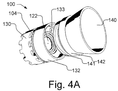
By way of example, Figs. 4A and 4B illustrate illumination device 100 with a
bottom
heat sink 130 and a top heat sink 132 and the board 104 disposed between
bottom and top heat
sinks 130, 132, along with the optical axis OA illustrated with a dotted line.
In one embodiment,
the board 104 may be bonded to the heat sinks 130 and 132 by way of thermal
epoxy.
Alternatively or additionally, the heat sinks 130, 132 may be screwed
together, via threads
-6-
CA 02702088 2010-04-08
WO 2009/052093 PCT/US2008/079806
130thread and 132threads, to clamp the board 104 between the heat sinks 130
and 132, as illustrated
in Fig. 4B. As can be seen in Fig. 4B, the board 104 may include thermal
contact areas 148,
sometimes referred to as heat spreaders on both the top and bottom surfaces
that are thermally
coupled to the top and bottom heat sinks 130 and 132, as indicated by the
arrows, e.g., using
thermal grease, thermal tape or thermal epoxy. As illustrated in Fig. 4B, the
sidewalls 110 are
formed using a separate insert 110;nsert piece that is inserted into and held
in heat sink 132, e.g.,
by thermal epoxy or by threads 110threads and 135, or by bolts. A removable
sidewall insert
110sidewall insert maybe positioned within insert 110insert and used to define
the sidewalls. The
sidewall insert 110sidewall insert may be e.g., manufactured from a material
referred to as Miro ,
type Miro 27 Silver, manufactured by Alanod, a German company. Additionally,
if desired, the
sidewall insert 110sidewall insert may be coated or impregnated (if sidewall
insert 110sidewall insert is
manufactured from plastic, ceramic, glass or other appropriate material) with
one or more
wavelength converting materials and/or highly diffuse reflective coatings,
such as is described in
reference to Fig. 4A as well as e.g., Figs. 15A and 15B. The adjustment of
color point of the
illumination device may be accomplished by replacing the sidewall insert
110sidewall insert, and/or
the window 122, which similarly may be coated or impregnated with one or more
wavelength
converting materials. Fig. 4B illustrates the side walls as having a linear
configuration, but it
should understood that side walls 110 may have any desired configuration,
e.g., curved, non-
vertical, beveled etc. In one embodiment, when the insert 110insert is
inserted into heat sink 132
from the top, an additional heat sink 142 may be coupled to top heat sink 132
and used to clamp
the insert 110insert in position in the heat sink 132. It should be understood
that the additional
heat sink 142 is optional. When the insert 110insert is inserted into heat
sink 132 from the bottom,
the bottom heat sink 130 may clamp the insert 110insert in position.
Alternatively, the sidewalls
110 may be integrally formed from heat sink 132. The window 122 may be mounted
in the
insert 110insert, e.g., using glue or clamps, such as clamping it between the
insert 110insert and a
heat sink 142 or 132. The bottom heat sink may include an aperture 130aperture
so that electrical
connections can be made to the board 104. An optical element, such as a
diffuser or reflector
140 may be removably coupled to the top heat sink 132, e.g., by means of
threads 133 and 141 or
a clamp or other appropriate mechanism. In one embodiment, the reflector 140
(Fig. 4A) may be
integrally formed from the additional heat sink 142 or may be mounted to the
heat sink 142, e.g.,
at the tapered walls 142taper of the heat sink 142 (Fig. 4B).
-7-
CA 02702088 2010-04-08
WO 2009/052093 PCT/US2008/079806
The LED board 104 is a board upon which is mounted one or more LED die or
packaged
LEDs. The board may be an FR4 board, e.g., that is 0.5mm thick, with
relatively thick copper
layers, e.g., 30 m to 100 m, on the top and bottom surfaces that serve as
thermal contact areas.
The board 104 may also include thermal vias. Alternatively, the board 104 may
be a metal core
printed circuit board (PCB) or a ceramic submount with appropriate electrical
connections.
Other types of boards may be used, such as those made of alumina (aluminum
oxide in ceramic
form), or aluminum nitride (also in ceramic form). The side walls 110 may be
thermally coupled
to the board 104 to provide additional heat sinking area.
For good cooling of the LEDs, a thermal contact area of at least 50 square
millimeter, but
preferably 100 square millimeter should be used per one watt going into the
LEDs on the board.
For example, in the case when 12 LEDs are used, a 600 to 1200 square
millimeter heatsink
contact area should be used. By using contact areas on both sides of the
boards the diameter of
the board can be reduced from 60 to 40 mm, which reduces the cost of the
board, but also
decreases the total size and volume of the illumination device, and makes it
much easier to use it
in existing lighting fixture designs.
Referring back to Fig. 3, the reflective plate 106 may be mounted on the top
surface of
the board 104, around the LEDs 102. The reflective plate 106 may be highly
reflective so that
light reflecting downward in the cavity 101 is reflected back generally
towards the output port
120. Additionally, the reflective plate 106 may have a high thermal
conductivity, such that it
acts as an additional heat spreader. By way of example, the reflective plate
106 may be
manufactured from a material including enhanced Aluminum. The reflective plate
106 may not
include a center piece between the LEDs 102, but if desired, e.g., where a
large number of LEDs
102 are used, the reflective plate 106 may include a portion between the LEDs
102 or
alternatively a central diverter, such as that illustrated in Figs 14A, 14B
and 19A. The thickness
of the reflective plate 106 may be approximately the same thickness as the
submounts of the
LEDs 102 or slightly thicker. The reflective plate might alternatively be made
from a highly
reflective thin material, such as VikuitiTM ESR, as sold by 3M (USA), which
has a thickness of
65 m, in which holes are punched at the light output areas of the LEDs, and
which is mounted
over the LEDs, and the rest of the board 104. The side walls 110 and the
reflective plate 106
may be thermally coupled and may be produced as one piece if desired. The
reflective plate 106
may be mounted to the board 104, e.g., using a thermal conductive paste or
tape. In another
-8-
CA 02702088 2010-04-08
WO 2009/052093 PCT/US2008/079806
embodiment, the top surface of the board 104 itself is configured to be highly
reflective, so as to
obviate the need for the reflective plate 106. Alternatively, a reflective
coating might be applied
to board 104, the coating composed of white particles e.g. made from Ti02,
ZnO, or BaSO4
immersed in a transparent binder such as an epoxy, silicone, acrylic, or N-
Methylpyrrolidone
(NMP) materials. Alternatively, the coating might be made from a phosphor
material such as
YAG:Ce. The coating of phosphor material and/or the Ti02, ZnO or GaSO4
material may be
applied directly to the board 104 or to, e.g., the reflective plate 106, for
example, by screen
printing. Typically in screen printing small dots are deposited. The dots
might be varied in size
and spatial distribution to achieve a more uniform or more peaked luminance
distribution over
the window 122, to facilitate either more uniform or more peaked illumination
patterns in the
beam produced by an embodiment such as that shown in Fig. 4A.
As illustrated in Figs. 1 and 2, multiple LEDs 102 may be used in the
illumination device
100. The LEDs 102 are positioned rotationally symmetrically around the optical
axis of the
illumination device 100, which extends from the center of the cavity 101 at
the reflective plate
106 (or board 104) to the center of the output port 110, so that the light
emitting surfaces or p-n
junctions of the LEDs are equidistant from the optical axis. The illumination
device 100 may
have more or fewer LEDs, but six (6) to ten (10) LEDs has been found to be a
useful quantity of
LEDs 102. In one embodiment, twelve (12) or fourteen (14) LEDs are used. When
a large
number of LEDs is used, it may be desirable to combine the LEDs into multiple
strings, e.g., two
strings of six (6) or seven (7) LEDs, in order to maintain a relatively low
forward voltage and
current, e.g., no more than 24V and 700mA. If desired, a larger number of the
LEDs may be
placed in series, but such a configuration may lead to electrical safety
issues.
In one embodiment, the LEDs 102 are packaged LEDs, such as the Luxeon Rebel
manufactured by Philips Lumileds Lighting. Other types of packaged LEDs may
also be used,
such as those manufactured by OSRAM (Ostar package), Luminus Devices (USA), or
Tridonic
(Austria). As defined herein, a packaged LED is an assembly of one or more LED
die that
contains electrical connections, such as wire bond connections or stud bumps,
and possibly
includes an optical element and thermal, mechanical, and electrical
interfaces. The LEDs 102
may include a lens over the LED chips. Alternatively, LEDs without a lens may
be used. LEDs
without lenses may include protective layers, which may include phosphors. The
phosphors can
be applied as a dispersion in a binder, or applied as a separate plate. Each
LED 102 includes at
-9-
CA 02702088 2010-04-08
WO 2009/052093 PCT/US2008/079806
least one LED chip or die, which may be mounted on a submount. The LED chip
typically has a
size about Imm by Imm by 0.5mm, but these dimensions may vary. In some
embodiments, the
LEDs 102 may include multiple chips. The multiple chips can emit light similar
or different
colors, e.g., red, green, and blue. In addition, different phosphor layers may
be applied on
different chips on the same submount. The submount may be ceramic or other
appropriate
material and typically includes electrical contact pads on a bottom surface,
which is coupled to
contacts on the board 104. Alternatively, electrical bond wires may be used to
electrically
connect the chips to a mounting board, which in turn is connected to a power
supply. Along with
electrical contact pads, the LEDs 102 may include thermal contact areas on the
bottom surface of
the submount through which heat generated by the LED chips can be extracted.
The thermal
contact areas are coupled to a heat spreading layer on the board 104.
The LEDs 102 can emit different or the same colors, either by direct emission
or by
phosphor conversion, e.g., where the different phosphor layers are applied to
the LEDs. Thus,
the illumination device 100 may use any combination of colored LEDs 102, such
as red, green,
blue, amber, or cyan, or the LEDs 102 may all produce the same color light or
may all produce
white light. For example, the LEDs 102 may all emit either blue or UV light
when used in
combination with phosphors (or other wavelength conversion means), which may
be, e.g., in or
on the window 122 of the output port 120, applied to the inside of the side
walls 110, or applied
to other components placed inside the cavity (not shown), such that the output
light of the
illumination device 100 has the color as desired. The phosphors may be chosen
from the set
denoted by the following chemical formulas: Y3A15012:Ce, (also known as
YAG:Ce, or simply
YAG) (Y,Gd)3A15012:Ce, CaS:Eu, SrS:Eu, SrGa2S4:Eu, Ca3(Sc,Mg)2Si3O12:Ce,
Ca3Sc2Si3O12:Ce, Ca3Sc2O4:Ce, Ba3Si6O12N2:Eu, (Sr,Ca)A1SiN3:Eu, CaAlSiN3:Eu.
In one embodiment a YAG, phosphor is used on the side walls 110 and the
reflective
plate 106 at the bottom of the cavity 101, and a red emitting phosphor such as
CaAlSiN3:Eu, or
(Sr,Ca)A1SiN3:Eu is used on the window 122 of the output port 120. By choosing
the shape and
height of the side walls that define the cavity, and selecting which of the
parts in the cavity will
be covered with phosphor or not, and by optimization of the layer thickness of
the phosphor
layer on the window, the color point of the light emitted from the module can
be tuned as
desired.
-10-
CA 02702088 2010-04-08
WO 2009/052093 PCT/US2008/079806
Fig. 5 illustrates an exploded perspective view of another embodiment of a
solid state
illumination device 100', that is similar to the illumination device 100 shown
in Fig. 3, except
that the illumination device 100' includes additional LEDs 102 and differently
shaped side walls
110', output port 120' and window 122'. As can be seen in Fig. 5, the
illumination device 100'
includes hexagonal tubular side walls 110', which define a hexagonal output
port 120' and the
window 122'. It should be understood that the side walls may have other
configurations,
including square, pentagonal, or other polygonal shapes. The use of square,
pentagonal or
hexagonal cross sectional tubes to from the side walls of the illumination
device may provide
superior light mixing relative to a circular cross sectional tube. With the
use of a larger number
of LEDs, it is desirable for the side walls to have a polygonal cross section
with the number of
sides equal to, or an integer multiple of, the number of LEDs. For example,
with the use of
twelve (12) LEDs, a twelve sided polygon, i.e., a dodecagon, or a polygon with
24 or 36 sides
may be used. Moreover, it may be desirable to use an insert for the side
walls, so that the
number of sides may easily be changed, e.g., if the number of LEDs is altered,
without requiring
modification of other parts of the device.
As illustrated in Fig. 5, the illumination device 100' includes six (6) LEDs
102 with
rotationally symmetric placement. The reflective plate 106' is configured to
accommodate the
six LEDs 102. As can be seen in Fig. 5, the reflective plate 106' includes a
center portion 106'a
that is configured to be placed between the center of the LEDs 102.
Fig. 6 illustrates a side view of an application of the illumination device in
a down light
configuration or other similar configuration, such as a spot lamp for task
lighting. A portion of
the side walls 110 are shown cut out so that the LEDs 102 inside the light
mixing cavity 101 are
visible. As illustrated, the illumination device 100 further includes a
reflector 140 for
collimating the light that is emitted from the light mixing cavity 101. The
reflector 140 may be
made out of a thermal conductive material, such as a material that includes
aluminum or copper
and may be thermally coupled to a heat spreader on the board 104, as discussed
in reference to
Fig. 4A, along with or through the side walls 110. Heat flows through
conduction through heat
spreaders attached to the board, the thermally conductive side wall, and the
thermal conductive
reflector 140, as illustrated by arrow 143. Heat also flows via thermal
convection over the
reflector 140 as illustrated by arrows 144. The heat spreader on the board may
be attached to
-11-
CA 02702088 2010-04-08
WO 2009/052093 PCT/US2008/079806
either the light fixture, or to a heat sink, such as heat sink 130 and/or heat
sink 132, shown in Fig.
3 and 4A.
Figs. 7A and 7B illustrate different placement patterns of the LEDs 102 on a
board 104',
both of which retain rotationally symmetry to the optical axis at the center.
In Fig. 7A, the LEDs
102 are configured radially on the board 104, so that there is rotational
symmetry around a
central axis 103, i.e., all the LED chips, in particular the p-n junctions,
are all approximately the
same distance R from the central axis 103. Fig. 7B shows the LEDs 102 placed
with orthogonal
orientations on the board 104' (without the overlying reflective plate 106').
The use of
orthogonal orientations of the LEDs is preferred by some component pick and
place machines.
As can be seen in Fig. 7B, however, the LED chips are all approximately the
same distance R'
from the central axis 103, and are therefore rotational symmetric around a
central axis 103.
Fig. 7C illustrates another layout of four (4) LEDs 102' on a board 104",
where the
LEDs 102' do not include a lens. As can be seen, the LEDs 102' may include
multiple chips
102chip per LED submount 102submount. The groups of multiple chips have a
rotationally
symmetry to the center as indicated by the broken lines. In some embodiments,
e.g., as
illustrated in Figs. 7A and 7B, a lens may be used, e.g., to protect the chips
and to improve light
output. The chips 102chip may emit different colored light, e.g., red (R),
green (G), blue (B) and
phosphor converted (W) light as indicated in Fig. 7C. As illustrated, each
colored chip 102chip
may have a different relative position on the submount 102submount, which may
improve color
uniformity. Alternatively, chips 102chip may be the same color, e.g., blue or
UV, to pump a
phosphor (red, green, blue, yellow, amber, etc.) directly attached to the chip
or located elsewhere
in the illumination device. Thus, any desired combination of colored light
emitting chips and
phosphors may be used.
Figs. 8A, 8B, and 8C, respectively illustrate top plan views of a three LED
board 104,
five LED board 104f,,,e, and seven LED board 104Seõen (sometimes collectively
referred to as
boards 104), which may be used with the illumination device 100. The outline
of the LEDs 102
are shown with broken lines. The boards 104 include electrical pads 142 to
which the electrical
pads on the LEDs 102 are connected. The electrical pads 142 are electrically
connected by a
metal, e.g., copper, trace to a contact 144, to which a wire, bridge or other
external electrical
source is connected. In some embodiments, the electrical pads 142 may be vias
through the
board 104 and the electrical connection is made on the opposite side, i.e.,
the bottom, of the
-12-
CA 02702088 2010-04-08
WO 2009/052093 PCT/US2008/079806
board. The boards 104 may include an aperture 146 in the center that may be
used allow access
from the bottom side of the board. The boards 104 also include heat spreader
148, which may be
copper or other appropriate metal. The heat spreader 148 extracts heat from
the LEDs 102 and
transports heat from the top of the board 104 to the bottom of the board 104
by thermal vias 150.
Additionally, the heat spreader 148 may extend around the edge of the aperture
146 to assist in
transporting heat to the bottom of the board 104.
Fig. 9A illustrates a perspective view of a illumination device 200, which is
similar to
illumination device 100, but in which reflective plate 106 is replaced by a
portion of the side
walls 210. The side walls 210 may be constructed from a single element, such
as Miro
material from Alanod, and joined together at joint 211. Bottom portions 212 of
the side walls are
bent to fit in between the LEDs 102 at the board 204. The use of a single
element for the side
walls 210 and the bottom reflective surface (in place of the reflective plate
106) advantageously
reduces cost.
Fig. 9B illustrates a top view of the illumination device 200 along with a
heat spreader
220 coupled to the side walls 210. The heat spreader 220 may be formed from,
e.g., corrugated
sheet metal, and includes ribs 222 that are in thermal contact with the side
walls 210. The heat
spreader 220 may also be in contact with the board 204. The heat spreader 220
may include
perforated holes to enhance heat exchange through convection. In addition, the
heat spreader
220 may be made of a black material or painted black to maximize emission by
radiation.
Figs. 10A and 10B illustrate top and bottom perspective views of a
illumination device
200' similar to the illumination device 200 shown in Figs. 9A and 9B.
Illumination device 200',
however, uses a heat sink 230 having radial fins 232 and an optically
reflective hexagonal cavity
234 in the center. The heat sink 230 may be extruded, casted, molded, machined
or otherwise
manufactured from a thermally conductive material, such as aluminum. In one
embodiment,
interchangeable side walls 210" may be inserted into the center cavity 234" of
the heat sink
230", as illustrated in Fig. 10C, which shows a top perspective view of a
illumination device
200" similar to that shown in Fig. 10A. Interchangeable side walls 210" have
different
configurations for the light mixing cavity 201', i.e., different shapes, but
are configured to be
inserted into or otherwise mounted to the heat sink 230", thereby obviating
the need to redesign
the heat sink 230" itself to accommodate different side walls.
-13-
CA 02702088 2010-04-08
WO 2009/052093 PCT/US2008/079806
Referring back to Figs. 10A and 10B, the corners of the center cavity 234 may
have a
bending radius to facilitate the use of a sheet metal insert such as side
walls 210. Alternatively,
the walls inside the center cavity 234 of the heat sink 230 may be made highly
reflective, e.g., by
applying a highly reflective coating to the inside of the heat sink 230. In
one embodiment, a
highly reflective white paint, or (protected and/or enhanced reflectivity)
metal or dichroic
coatings may be applied to the inside of the heat sink 230. If desired, the
inside wall of the heat
sink 230 might by partially or completely covered with a phosphor material as
well. As
illustrated in Fig. 10B, the heat sink 230 may be thermally coupled to the
heat spreader on the
board 204, e.g., by screwing, or gluing, or by clamping. A thermal paste or
thermal tape may be
used between the heat sink 230 and the heat spreader on the board 204.
In one embodiment, the height of heat sink 230 may be approximately 12 mm, and
the
distance between opposite walls of the center (indicated by the letter D) may
be approximately
the same, i.e., 12 mm. The surface area of the heat sink 230 with these
dimensions may be
approximately 3500 mm2, i.e., approximately 5.4 square inches, which is one
parameter of the
cooling capacity of the heat sink 230 and provides a total dissipation of
power of approximately
2 Watts. For higher power illumination device, e.g., approximately 10 Watts,
the heat sink 230
can be made longer to increase the cooling power. A longer configuration of
the heat sink 230
has the benefit that the mixing length of the optical cavity 201 of the
illumination device 200' is
increased which provides a better uniformity for the light distribution at the
output port. With
the use of the heat sink 230 coupled to (or forming) the side walls of the
illumination device
200', the functions of optical mixing and cooling are combined, resulting in a
illumination device
with reduced length relative to devices that separate the heat sink from the
side walls. If desired,
other shapes may be used for the optical cavity 201, such as octagonal,
pentagonal or other
polygonal shapes. Further, the center cavity 234 may be tapered so that the
distance D between
opposite walls near the LEDs is different than, e.g., greater or lesser than,
the distance between
the opposite walls at a location farther from the LEDs.
Figs. 11A and 11B illustrate a side view and a top view of illumination device
200' with
heat sink 230 and a reflector 240. The reflector 240 may be made of a metal
such as aluminum,
copper or alloys thereof, and is thermally coupled to the heat sink 230 to
assist in the heat
dissipation. An advantage of this configuration is that no additional
diffusers are required to
homogenize the light, which increases the throughput efficiency.
-14-
CA 02702088 2010-04-08
WO 2009/052093 PCT/US2008/079806
Fig. 12 illustrates a bottom perspective view of the illumination device 200'
with the
reflector 240 and with an additional heat sink 250 thermally coupled to the
bottom surface of the
board 204. The heat sink 250 may consist of a plurality of pins or other
similar configuration.
Using a second heat sink 250 permits the LEDs 102 to be driven at higher
power, and also allows
for different heat sink designs, so that the cooling capacity is less
dependent on the orientation of
the heat sink. In addition, fans or other solutions for forced cooling may be
used to remove the
head from the device.
Fig. 13 illustrates a perspective view of another embodiment of a illumination
device
300, similar to illumination device 200 with an integrated color mixing cavity
310, heat sink 320,
and reflector 312. A portion of the heat sink 320 is cut away in Fig. 13 to
show the board 304
with LEDs 102 and a bottom cavity 308 that is formed by the heat sink 320
extending below the
board 304. The bottom cavity 308 may be used for housing electronic or electro-
mechanical
parts to drive the LEDs 102. Alternatively, the bottom cavity 308 may house a
fan. The
illumination device 300 also includes a reflector 312 that is coupled to the
heat sink 320. The
reflector 312 may be removably coupled, e.g., by screw of clamp.
Fig. 14A illustrates a perspective view of another embodiment of a
illumination device
350, with reflective side walls 360 that have a hexagonal configuration that
is tapered so that the
distance between opposite side walls is less at the bottom of the side walls,
i.e., at the reflective
plate 356, then at the top of the side walls, i.e., at the output port 362.
Illumination device 350 is
illustrated in Fig. 14A with a tapered hexagonal center reflector 352, which
is configured to
redirect light emitted into large angles from the LEDs 102 into narrower
angles with respect to
normal to the board 354. In other words, light emitted by LEDs 102 that is
close to parallel to
the board 354 is redirected upwards toward the output port 362 so that the
light emitted by the
illumination device has a smaller cone angle compared to the cone angle of the
light emitted by
the LEDs directly. By reflecting the light into narrower angles, the
illumination device 350 can
be used in applications where light under large angles is to be avoided, for
example, due to glare
issues (office lighting, general lighting,), or due to efficiency reasons
where it is desirable to send
light only where it is needed and most effective (task lighting, under cabinet
lighting.)
Moreover, the efficiency of light extraction is improved for the illumination
device 350 as light
emitted in large angles undergoes less reflections in the light mixing cavity
351 before reaching
the output port 362 compared to a device without the center reflector 352.
This is particularly
-15-
CA 02702088 2010-04-08
WO 2009/052093 PCT/US2008/079806
advantageous when used in combination with a light tunnel or integrator, as it
is beneficial to
limit the flux in large angles due to light being bounced around much more
often in the mixing
cavity, thus reducing efficiency. The reflective plate 356 on the board 354
may be used as an
additional heat spreader.
Fig. 14B illustrates another perspective view of illumination device 350, with
a window
364 over the output port 362, which may act as a diffuser, and a center dome
reflector 353 that is
configured to distribute the light from the LEDs 102 over the diffuser window
364. The dome
reflector 353 may have either diffuse or mirror like reflective properties.
The window 364 may
include one or more phosphors. A dichroic mirror 366 layer may be coupled to
the window 364
between the LEDs 102 and the phosphor in or on the window 364. The dichroic
mirror 366 may
be configured to mostly reflect blue light and transmit light with longer
wavelengths, which is
generated by the phosphor conversion.
Fig. 14C illustrates another perspective view of illumination device 350 with
hexagonal
side wall extensions 361 attached to the tapered side walls 360. A portion of
the side wall
extensions 361 are shown cut away in Fig. 14C. The side wall extensions 361
are less tapered
than the tapered side walls 360 and in one embodiment may have no taper. A
higher transfer
efficiency is achieved through the light mixing cavity 351 by pre-collimation
of the light using
the tapered side walls 360.
Figs. 15A and 15B illustrate perspective views of the side walls 110 with
patterns of
different types of phosphor, e.g., a red phosphor and a green phosphor, inside
the cavity 101. In
one embodiment, the illumination device may include different types of
phosphors that are
located at different areas of the light mixing cavity 101. For example, red
and green phosphors
may be located on the side walls 110 or the board 104 and a yellow phosphor
may be located on
the top or bottom surfaces of the window or embedded within the window. In one
embodiment,
a central reflector such as that shown in Fig. 14C may have patterns of
different types of
phosphor, e.g., a red phosphor on a first area and a green phosphor on a
separate second area. In
another embodiment, different types of phosphors, e.g., red and green, may be
located on
different areas on the sidewalls 110. For example, one type of phosphor 110R
may be patterned
on the sidewalls 110 at a first area, e.g., in stripes, spots, or other
patterns, while another type of
phosphor 110G is located on a different second area of the sidewall. If
desired, additional
phosphors may be used and located in different areas in the cavity 101.
Additionally, if desired,
-16-
CA 02702088 2010-04-08
WO 2009/052093 PCT/US2008/079806
only a single type of wavelength converting material may be used and patterned
in the cavity
101, e.g., on the sidewalls, where the areas indicated by 110G have no
phosphor and are, e.g.,
reflective or diffusing. An unanticipated result of placing the different
phosphors in separate
areas is that the light quality and performance results are improved compared
to a device in
which the phosphors are combined before applying. Table 1 shows the measured
difference in
performance between separated phosphors and mixed phosphors.
Cavity coated with
spatially separated Cavity coated with a
phosphors mixed phosphors
Measured optical power 1.27 W 1.25 W
Measured color rendering index Ra 82 Ra 77
Measured color temperature 2917 K 2960 K
TABLE 1
The second column in Table 1 shows the results of an experiment where the side
walls of
a cavity, similar to that shown in Fig. 19A, were coated with alternating
stripes of two
phosphors. The height of the cavity in this experiment was approximately 6 mm,
while the
diameter at the bottom was 22 mm, and the diameter at the top 18 mm. In this
particular
experiment, a flat specular Miro (as produced by Alanod, type Miro 27 Silver)
mirror was used
at the bottom of the cavity, with a diameter of 13.5 mm. The phosphors used
were a YAG:Ce
phosphor, and a SrCaAlSiN3:Eu phosphors, which were placed in vertical stripes
approximately
2mm and 3mm, respectively. At approximately same color points and correlated
color
temperatures, we achieved a slightly higher output (1.27W versus 1.25W), and a
large gain in the
color rendering index. A color rendering index of Ra 80 is generally accepted
is the minimum
for many commercial lighting applications. Additionally, applying the
phosphors in different
areas, simplifies the control of the color balance, e.g., the area of one
phosphor can be increased
while maintaining the area of the other phosphor the same. Alternatively, a
first phosphor can be
extended to cover part of the second phosphor.
In an embodiment, a single type of wavelength converting material may be
patterned on
the sidewall, which may be, e.g., the sidewall insert 110sidewall insert shown
in Fig. 4B. By way of
example, a red phosphor may be patterned on different areas of the sidewall
insert 110sidewall insert
and a yellow phosphor may cover the window 122, shown in Fig. 4B. The coverage
and/or
concentrations of the phosphors may be varied to produce different color
temperatures. Table 2
-17-
CA 02702088 2010-04-08
WO 2009/052093 PCT/US2008/079806
shows the percentage of coverage and concentration (by volume) of the red
phosphor on a
sidewall insert 110sidewall insert and a yellow phosphor covering 100% of the
window 122 to
produce the indicated color temperature, with a blue light of 455nm. It should
be understood that
the coverage area of the red and/or the concentrations of the red and yellow
phosphors will need
to vary to produce the desired color temperatures if the blue light produced
by the LEDs 102
varies from 455nm. The color performance of the LEDs 102, red phosphor on the
insert sidewall
insert 110sidewall insert and the yellow phosphor on the window 122 may be
measured before
assembly and selected based on performance so that the assembled pieces
produce the desired
color temperature. The thickness of the red phosphor may be, e.g., between 40
m to 80 m and
more specifically between 60 m to 70 m, while the thickness of the yellow
phosphor may be,
e.g., between 50 m to 100 m and more specifically between 70 m to 90 m.
Color % of coverage Concentration Concentration
Temperature (Red) (Red) (Yellow)
4000 K 40% 5% 13.5% 2% 20% 3%
3000 K 70% 5% 16% 2% 26% 3%
2700 K 100% 17% 2% 29% 3%
TABLE 2
In another embodiment, a single continuous layer of red phosphor may be used
on the
sidewalls, e.g., on the sidewall insert 110sidewallinsert shown in Fig. 4B.
The continuous red
phosphor, which covers 100% of the sidewall, and a yellow phosphor covering
the window 122
may have different concentrations to produce different color temperatures.
Table 3 shows the
concentrations (by volume) of a red phosphor on a sidewall insert 110sidewall
insert and a yellow
phosphor covering 100% of the window 122 to produce the indicated color
temperature, with a
blue light of 455nm. It should be understood that the concentrations of the
red and yellow
phosphors will need to vary to produce the desired color temperatures if the
blue light produced
by the LEDs 102 varies from 455nm. The color performance of the LEDs 102, red
phosphor on
the insert sidewall insert I IOsidewall insert and the yellow phosphor on the
window 122 may be
measured before assembly and selected based on performance so that the
assembled pieces
produce the desired color temperature. The thickness of the red phosphor may
be, e.g., between
70 m to 110 m and more specifically between 85 m to 95 m, while the thickness
of the yellow
phosphor may be, e.g., between 50 m to 100 m and more specifically between 70
m to 90 m.
-18-
CA 02702088 2010-04-08
WO 2009/052093 PCT/US2008/079806
Color Concentration Concentration
Temperature (Red) (Yellow)
4000 K 2.5% 2% 20% 3%
3000 K 8% 2% 26% 3%
2700 K 16% 2% 29% 3%
TABLE 3
Fig. 16 illustrates another embodiment of a illumination device 350a, which is
similar to
illumination device 350 shown in Fig. 14A, except each LED 102 in illumination
device 350a is
surrounded by a separate individual side wall reflector 360a, which may have a
parabolic,
compound parabolic, elliptical shape, or other appropriate shape. The light
from illumination
device 350a is collimated from large angles into smaller angles, e.g., from a
2 x 90 degree angle
to a 2 x 60 degree angle, or a 2 x 45 degree beam. The illumination device
350a can be used as a
direct light source, for example, as a down light or an under the cabinet
light, or it can be used to
inject the light into a light mixing cavity, e.g., such as that defined by
side walls 210 as shown in
Fig. 9A and 9B. The illumination device 350a may be thermally coupled between
a top and
bottom heat sinks, such as that illustrated in Fig. 4A.
Fig. 17 illustrates a plurality of illumination devices 350 that are arranged
together to
form a large lighting module 380. The center illumination device 350
illustrated in Fig. 17 is
shown with the window 364 partly cut away to illustrated the underlying LEDs
102. If desired,
the illumination devices 350 may be arranged in different configurations to
form, e.g., a linear
structure, a semi-circular or circular structure, a hexagonally closely packed
structure, or other
desired configurations.
Fig. 18 illustrates a illumination device 350 with a hexagonal reflector 390.
The
hexagonal reflector 390 is illustrated with a cut-away portion 392 to provide
a view of the
illumination device 350, which is illustrated with a partially cut-away window
364. The
hexagonal reflector 390 may be made from a highly thermally conductive
material, e.g., sheet
metal, and may be thermally coupled to the LED board 354 or a heat sink 610,
as for example,
illustrated in Fig. 19A. The use of a hexagonal reflector 390 is advantageous
as it permits
multiple reflectors to be stacked together to form a compact array of
collimators. Additionally, a
reflector with a hexagonal configuration (as opposed to a circular
configuration) better facilitates
uniformity (color and brightness) coming out of the reflector.
-19-
CA 02702088 2010-04-08
WO 2009/052093 PCT/US2008/079806
Fig. 19A illustrates a cross sectional view of another embodiment of a
illumination
device 600, similar to illumination device 100, shown in Figs. 1 and 2.
Illumination device 600
is illustrated with LEDs 102 mounted on a board 604 that is mounted on a heat
sink 608.
Additionally, side walls 610 are shown as tapered so that the cross-sectional
area of the cavity
601 at the bottom, e.g., proximate to the LEDs 102, is greater than the cross-
sectional area of the
cavity 601 at the top, e.g., distal to the LEDs 102. As with illumination
device 100, the side
walls 610 of illumination device 600 may define a cavity 601 with a continuous
shape, e.g.,
circular (elliptical) as illustrated in Fig. 19B or a non-continuous polygonal
shape, as illustrated
in Fig. 19C, or a combination thereof.
Illumination device 600 may further include a diverter 602, which may be
placed
centrally in the cavity 601. The use of this diverter 602 helps to improve the
efficiency of the
illumination device 600 by redirecting light from the LEDs 102 towards the
window 622. In Fig.
19A the diverter 602 is illustrated as having a cone shape, but alternative
shapes may be used if
desired, for example, a half dome shape, or a spherical cap, or aspherical
reflector shapes.
Moreover as illustrated in Figs. 19B and 19C, the diverter 602 may have
various shapes in plan
view. The diverter 602 can have a specular reflective coating, a diffuse
coating, or can be coated
with one or more phosphors. The height of the diverter 602 may be smaller than
the height of
the cavity 601 (e.g., approximately half the height of the cavity 601) so that
there is a small space
between the top of the diverter 602, and the window 622.
In one embodiment a YAG phosphor is used on the side walls 610 and the board
604 at
the bottom of the cavity 601, and a red emitting phosphor such as CaAlSiN3:Eu,
or
(Sr,Ca)A1SiN3:Eu is used on the window 622. By choosing the shape of the side
of the cavity,
and selecting which of the parts in the cavity will be covered with phosphor
or not, and by
optimization of the layer thickness of the phosphor layer on the window, the
color point of the
light emitted from the module can be tuned to the color as desired by the
customers.
In one embodiment, a blue filter 622filter may be coupled to the window 622 to
prevent
too much blue light from being emitted from the illumination device 600. The
blue filter 622fiiter
may be an absorbing type or a dichroic type, with no or very little
absorption. In one
embodiment, the filter 622filter has a transmission of 5% to 30% for blue,
while a very high
transmission (greater than 80%, and more particularly 90% or more) for light
with longer
wavelengths.
-20-
CA 02702088 2010-04-08
WO 2009/052093 PCT/US2008/079806
Figs. 20A, 20B, 20C, and 20D illustrate various configurations of the window
622 shown
in cross sectional views. The window 622 is placed into or on top of the side
wall 610. In these
cross sectional views only part of the side wall 610 is shown.
In Fig. 20A, the window 622 is shown mounted on top of the side wall 610. It
can be
beneficial to seal the gap 623 between the window 622 and the side wall 610 to
form a
hermetically sealed cavity 601 (Fig. 19A), such that no dust or humidity can
enter the cavity 601.
A sealing material may be used to fill the gap 623 between the window 622 and
the side wall
610, as for example an epoxy or a Silicone material. It may be beneficial to
use a material that
remains flexible over time due to the differences in thermal expansion
coefficients of the
materials of the window 622 and side wall 610. As an alternative, the window
622 might be
made of glass or a transparent ceramic material, and soldered onto the side
walls 610. In that
case, the window 622 may be plated at the edges with a metallic material, such
as aluminum, or
silver, or copper, or gold, and solder paste is applied in between the side
wall 610 and window
622. By heating the window 622 and the side wall 610, the solder will melt and
provide a good
connection between the side wall 610 and window 622.
In Fig. 20B, the window 622 has an additional layer 624 on the inside surface
of the
window, i.e., the surface facing the cavity 601. The additional layer 624 may
contain either
white diffusing particles, or particles with wavelength converting properties
such as phosphors.
The layer 624 can be applied to the window 622 by screen printing, spray
painting, or powder
coating. For screen printing and spray painting, typically the particles are
immersed in a binder,
which can by a polyurethane based lacquer, or a Silicone material. For powder
coating a binding
material is mixed into the powder mix in the form of small pellets which have
a low melting
point, and which make a uniform layer when the window 622 is heated, or a base
coat is applied
to the window 622 to which the particles stick during the coating process.
Alternatively, the
powder coating may be applied using an electric field, and the window and
phosphor particles
baked in an oven so that the phosphor permanently adheres to the window. The
thickness and
optical properties of the layer 624 applied to the window 622 may be monitored
during the
powder coat process for example by using a laser and a spectrometer, and/or
detector, or and/or
camera, both in forward scatter and back scattered modes, to obtain the right
color and/or optical
properties.
-21-
CA 02702088 2010-04-08
WO 2009/052093 PCT/US2008/079806
In Fig. 20C the window 622 has two additional layers 624 and 626; one on the
inside of
the window and one on the outside of the window 622, respectively. The outside
layer 626 may
be white scattering particles, such as Ti02, ZnO, and/or BaSO4 particles.
Phosphor particles
may be added to the layer 626 to do a final adjustment of the color of the
light coming out of the
illumination device 600. The inside layer 624 may contain wavelength
converting particles, such
as a phosphor.
In Fig. 20D the window 622 also has two additional layers 624 and 628, but
both are on
the same inside surface of the window 622. While two layers are shown, it
should be understood
that additional layers may be used. In one configuration, layer 624, which is
closest to the
window 622, includes white scattering particles, such that the window appears
white if viewed
from the outside, and has a uniform light output over angle, and layer 628
includes a red emitting
phosphor. The surfaces of the side walls 610 and/or the board 604 may be
coated with a yellow
or green emitting phosphor.
The phosphor conversion process generates heat and thus the window 622 and the
phosphor, e.g., in layer 624, on the window 622 should be configured so that
they do not get too
hot. For this purpose, the window 622 may have a high thermal conductivity,
e.g., not less than
1W/(m K), and the window 622 may be thermally coupled to the side wall 610,
which serves as a
heat-sink, using a material with low thermal resistance, such as solder,
thermal paste or thermal
tape. A good material for the window is aluminum oxide, which can be used in
its crystalline
form, called Sapphire, as well in its poly-crystalline or ceramic form, called
Alumina.
Fig. 21 is a bottom view of the window 622 covered with a patterned layer 624
of
phosphors. A wedge or pie-shaped pattern may be used to form the layer 624, if
desired, using
two types of wavelength converting materials, where the wedges for example
have alternating
red emitting phosphor 624R and green emitting phosphor 624G. Using a radial
pattern as
illustrated in Fig. 21 may provide good color mixing when used in combination
with a reflective
collimator. Other patterns may be used if desired as for example small dots
with varying size,
thickness and density.
Figs. 22A and 22B illustrate the effect of the aperture size of the window 622
on the
beam angle produced by a reflector 640 placed on top of the illumination
device 600 (as
illustrated in Fig. 19A). The model used for the results of Figs. 22A and 22B
is based on a
-22-
CA 02702088 2010-04-08
WO 2009/052093 PCT/US2008/079806
compound parabolic concentrator design, which gives the smallest total angle
for the beam
coming out of the reflector. The total angle is the angle that light will be
emitted from the
reflector 640, such that is there will be no or very little light beyond this
angle. For down lights
for example, this total angle is typically in the range of 100 to 120 degrees
(60 degree cut-off
with the normal to the reflector opening), while for spot lamps this total
angle is more in the
range of 20 to 80 degrees.
Fig. 22A shows a cross sectional view of a reflector 640 that is a compound
parabolic
concentrator, where the concentrator is made out of a highly reflecting
material. Indicated is a
measure for the input diameter for the concentrator D, and the full beam angle
measurement 6,
and the output diameter Dout. Compound parabolic concentrators tend to be
tall, but they often
are used in a reduced length form, which increases the beam angle. The beam
angle as a
function of aperture size D is shown in Fig. 22B for two sizes of the output
diameter D0 of the
reflector 640, specifically an MR16 reflector lamp size, which has an output
diameter Doõr of
about 50 mm, and a PAR38 size, which has an output diameter Doõr of about 120
mm.
For the size of an MR16 lamp equivalent diameter reflector, typical aperture
size may be
in the range of 10 to 30 mm for spot lamps, while for an MR16 down-light the
aperture size may
be about 40 mm. For a PAR 38 equivalent diameter reflector, typical aperture
size is in the range
of 20 mm to 75 mm, e.g., 50mm, for spot lamps, while for the down-light
function for the
PAR38 the aperture size should be less than 100 mm.
The sizes for the apertures given here should be considered as maximum sizes,
as cut-off
angles tend to become wider. In addition, center beam intensity increases
proportional to the
area of the output of the reflector compared to the input area of the
reflector.
Fig. 23 illustrates a cross-sectional view of illumination device 600 that is
electronically
controllable to produce a desired color point. The color of the light output
of the illumination
device 600 (shown in Fig. 23) is changed by using at least two blue LEDs 102B
and 102b, where
one has a lower peak wavelength than the other LED. One blue LED 102b may have
a peak
wavelength in the range of 430 to 450 nm, while the other LED 102B may have a
peak
wavelength in the range of 450 nm to 470 nm. If more than two LEDs are used,
the LEDs with
the lower wavelength may be all electrically connected, and the LEDs with a
longer wavelength
may be electrically connected, but electrically separate from the lower LEDs
with the lower
-23-
CA 02702088 2010-04-08
WO 2009/052093 PCT/US2008/079806
wavelengths. A driver 670 is supplied, which can drive a different current
through the group
with lower wavelength LEDs 102b than the group with longer wavelength LEDs
102B. It should
be understood that the driver 670 is coupled to the LEDs 102B and 102b through
the board 604,
but that for illustrative purposes the connections are shown with a broken
lines in Fig. 23. As the
at least one phosphor in the illumination device 600 responds differently to
lower wavelength
light than higher wavelength light, a different color light output is
achieved, which can be
controlled by changing the current through the two different strings of LEDs
102B and 102b.
Optionally, a sensor 672 is used inside the cavity to measure the light output
or color of the
illumination device 600 and to provide that measurement in a feed back loop to
control the driver
670. The sensor 672 may be mounted at the output window of illumination device
600, or on the
bottom, top, or side of the cavity or inside a partially transparent diverter
602, as illustrated in
Fig. 23.
Although the present invention is illustrated in connection with specific
embodiments for
instructional purposes, the present invention is not limited thereto. It
should be understood that
the embodiments described herein may use any desired wavelength converting
materials,
including dyes, and are not limited to the use of phosphors. Various
adaptations and
modifications may be made without departing from the scope of the invention.
Therefore, the
spirit and scope of the appended claims should not be limited to the foregoing
description.
-24-