Note: Descriptions are shown in the official language in which they were submitted.
CA 02702487 2010-04-13
WO 2009/052371 PCT/US2008/080300
1
GROUND LEVEL PRECHARGE BIT LINE SCHEME FOR READ
OPERATION IN SPIN TRANSFER TORQUE
MAGNETORESISTIVE RANDOM ACCESS MEMORY
Field of Disclosure
[0001] Embodiments of the invention are related to random access memory (RAM).
More particularly, embodiments of the invention are related to read operations
in Spin
Transfer Torque Magnetoresistive Random Access Memory (STT-MRAM).
Background
[0002] Random access memory (RAM) is a ubiquitous component of modem digital
architectures. RAM can be stand alone devices or can be integrated or embedded
within
devices that use the RAM, such as microprocessors, microcontrollers,
application
specific integrated circuits (ASICs), system-on-chip (SoC), and other like
devices as
will be appreciated by those skilled in the art. RAM can be volatile or non-
volatile.
Volatile RAM loses its stored information whenever power is removed. Non-
volatile
RAM can maintain its memory contents even when power is removed from the
memory. Although non-volatile RAM has advantages in the ability to maintain
its
contents without having power applied, conventional non-volatile RAM has
slower read
/ write times than volatile RAM.
[0003] Magnetoresistive Random Access Memory (MRAM) is a non-volatile memory
technology that has response (read / write) times comparable to volatile
memory. In
contrast to conventional RAM technologies which store data as electric charges
or
current flows, MRAM uses magnetic elements. As illustrated in Figs IA and 1B,
a
magnetic tunnel junction (MTJ) storage element 100 can be formed from two
magnetic
layers 110 and 130, each of which can hold a magnetic field, separated by an
insulating
(tunnel barrier) layer 120. One of the two layers (e.g., fixed layer 110), is
set to a
particular polarity. The other layer's (e.g., free layer 130) polarity 132 is
free to change
to match that of an external field that can be applied. A change in the
polarity 132 of
the free layer 130 will change the resistance of the MTJ storage element 100.
For
example, when the polarities are aligned, Fig. IA, a low resistance state
exists. When
the polarities are not aligned, Fig. 1B, then a high resistance state exists.
The
CA 02702487 2010-04-13
WO 2009/052371 PCT/US2008/080300
2
illustration of MTJ 100 has been simplified and those skilled in the art will
appreciate
that each layer illustrated may comprise one or more layers of materials, as
is known in
the art.
[0004] Referring to Fig. 2A, a memory cell 200 of a conventional MRAM is
illustrated
for a read operation. The cell 200 includes a transistor 210, bit line 220,
digit line 230
and word line 240. The cell 200 can be read by measuring the electrical
resistance of
the MTJ 100. For example, a particular MTJ 100 can be selected by activating
an
associated transistor 210, which can switch current from a bit line 220
through the MTJ
100. Due to the tunnel magnetoresistive effect, the electrical resistance of
the MTJ 100
changes based on the orientation of the polarities in the two magnetic layers
(e.g., 110,
130), as discussed above. The resistance inside any particular MTJ 100 can be
determined from the current, resulting from the polarity of the free layer.
Conventionally, if the fixed layer 110 and free layer 130 have the same
polarity, the
resistance is low and a "0" is read. If the fixed layer 110 and free layer 130
have
opposite polarity, the resistance is higher and a "1" is read.
[0005] Referring to Fig. 2B, the memory cell 200 of a conventional MRAM is
illustrated for a write operation. The write operation of the MRAM is a
magnetic
operation. Accordingly, transistor 210 is off during the write operation.
Current is
propagated through the bit line 220 and digit line 230 to establish magnetic
fields 250
and 260 that can affect the polarity of the free layer of the MTJ 100 and
consequently
the logic state of the cell 200. Accordingly, data can be written to and
stored in the MTJ
100.
[0006] MRAM has several desirable characteristics that make it a candidate for
a
universal memory, such as high speed, high density (i.e., small bitcell size),
low power
consumption, and no degradation over time. However, MRAM has scalability
issues.
Specifically, as the bit cells become smaller, the magnetic fields used for
switching the
memory state increase. Accordingly, current density and power consumption
increase
to provide the higher magnetic fields, thus limiting the scalability of the
MRAM.
[0007] Unlike conventional MRAM, Spin Transfer Torque Magnetoresistive Random
Access Memory (STT-MRAM) uses electrons that become spin-polarized as the
electrons pass through a thin film (spin filter). STT-MRAM is also known as
Spin
Transfer Torque RAM (STT-RAM), Spin Torque Transfer Magnetization Switching
RAM (Spin-RAM), and Spin Momentum Transfer (SMT-RAM). During the write
operation, the spin-polarized electrons exert a torque on the free layer,
which can switch
CA 02702487 2010-04-13
WO 2009/052371 PCT/US2008/080300
3
the polarity of the free layer. The read operation is similar to conventional
MRAM in
that a current is used to detect the resistance / logic state of the MTJ
storage element, as
discussed in the foregoing. As illustrated in Fig. 3A, a STT-MRAM bit cell 300
includes MTJ 305, transistor 310, bit line 320 and word line 330. The
transistor 310 is
switched on for both read and write operations to allow current to flow
through the MTJ
305, so that the logic state can be read or written.
[0008] Referring to Fig. 3B, a more detailed diagram of a STT-MRAM cell 301 is
illustrated, for further discussion of the read / write operations. In
addition to the
previously discussed elements such as MTJ 305, transistor 310, bit line 320
and word
line 330, a source line 340, sense amplifier 350, read / write circuitry 360
and bit line
reference 370 are illustrated. As discussed above, the write operation in an
STT-
MRAM is electrical. Read / write circuitry 360 generates a write voltage
between the
bit line 320 and the source line 340. Depending on the polarity of the voltage
between
bit line 320 and source line 340, the polarity of the free layer of the MTJ
305 can be
changed and correspondingly the logic state can be written to the cell 301.
Likewise,
during a read operation, a read current is generated, which flows between the
bit line
320 and source line 340 through MTJ 305. When the current is permitted to flow
via
transistor 310, the resistance (logic state) of the MTJ 305 can be determined
based on
the voltage differential between the bit line 320 and source line 340, which
is compared
to a reference 370 and then amplified by sense amplifier 350. Those skilled in
the art
will appreciate the operation and construction of the memory cell 301 is known
in the
art. Additional details are provided, for example, in M. Hosomi, et al., A
Novel
Nonvolatile Memory with Spin Transfer Torque Magnetoresistive Magnetization
Switching: Spin-RAM, proceedings of IEDM conference (2005), which is
incorporated
herein by reference in its entirety.
[0009] The electrical write operation of STT-MRAM eliminates the scaling
problem
due to the magnetic write operation in MRAM. Further, the circuit design is
less
complicated for STT-MRAM. However, because both read and write operations are
performed by passing current through the MTJ 305, there is a potential for
read
operations to disturb the data stored in the MTJ 305. For example, if the read
current is
similar to or greater in magnitude than the write current threshold, then
there is a
substantial chance the read operation may disturb the logic state of MTJ 305
and thus
degrade the integrity of the memory.
CA 02702487 2010-04-13
WO 2009/052371 PCT/US2008/080300
4
SUMMARY
[0010] Exemplary embodiments of the invention are directed to systems,
circuits and
methods for read operations in STT-MRAM.
[0011] Accordingly, an embodiment of the invention can include a Spin Transfer
Torque Magnetoresistive Random Access Memory (STT-MRAM) array comprising a
plurality of bit cells, each coupled to one of a plurality of bit lines, word
lines and
source lines, and a plurality of precharge transistors, each corresponding to
one of the
plurality of bit lines, wherein the precharge transistors are configured to
discharge the
bit lines to ground, prior to a read operation.
[0012] Another embodiment of the invention can include a Spin Transfer Torque
Magnetoresistive Random Access Memory (STT-MRAM) array comprising a plurality
of bit cells, each coupled to one of a plurality of bit lines, word lines and
source lines, a
read mux configured to select one of the plurality of bit lines, and a
precharge transistor
coupled to an output of the read mux, wherein the precharge transistor is
configured to
discharge the selected bit line to ground, prior to a read operation.
[0013] Another embodiment of the invention can include a method for reading
memory
in a Spin Transfer Torque Magnetoresistive Random Access Memory (STT-MRAM)
comprising discharging at least a selected bit line to a ground potential
prior to a read
operation, selecting a bit cell on the selected bit line, and reading a value
of the bit cell
during the read operation.
BRIEF DESCRIPTION OF THE DRAWINGS
[0014] The accompanying drawings are presented to aid in the description of
embodiments of the invention and are provided solely for illustration of the
embodiments and not limitation thereof.
[0015] Figs. IA and lB are illustrations of a magnetic tunnel junction (MTJ)
storage
element.
[0016] Figs. 2A and 2B are illustrations of a Magnetoresistive Random Access
Memory
(MRAM) cell during read and write operations, respectively.
[0017] Figs. 3A and 3B are illustrations of Spin Transfer Torque
Magnetoresistive
Random Access Memory (STT-MRAM) cells.
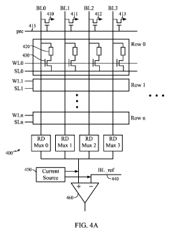
[0018] Fig. 4A is an illustration of a bit cell array of a STT-MRAM with a
ground level
precharge.
CA 02702487 2010-04-13
WO 2009/052371 PCT/US2008/080300
[0019] Fig. 4B is another illustration of a bit cell array of a STT-MRAM with
a ground
level precharge.
[0020] Fig. 5A is a graph illustrating the signal levels for a read operation
of a STT-
MRAM.
[0021] Fig. 5B is a graph illustrating another embodiment of the signal levels
for a read
operation of a STT-MRAM.
DETAILED DESCRIPTION
[0022] Aspects of embodiments of the invention are disclosed in the following
description and related drawings directed to specific embodiments of the
invention.
Alternate embodiments may be devised without departing from the scope of the
invention. Additionally, well-known elements of the invention will not be
described in
detail or will be omitted so as not to obscure the relevant details of
embodiments of the
invention.
[0023] The word "exemplary" is used herein to mean "serving as an example,
instance,
or illustration." Any embodiment described herein as "exemplary" is not
necessarily to
be construed as preferred or advantageous over other embodiments. Likewise,
the term
"embodiments of the invention" does not require that all embodiments of the
invention
include the discussed feature, advantage or mode of operation.
[0024] As discussed in the background, STT-MRAM uses a low write current for
each
cell, which is an advantage of this memory type over MRAM. However, cell read
current can approach or be higher than the write current threshold and thus
cause an
invalid write operation to happen. To mitigate this problem, the bit line (BL)
voltage
level during read operation can be held to a lower value than the write
threshold voltage.
[0025] Conventionally, the bit line (BL) voltage is precharged to a midpoint
voltage
(e.g., 0.4V). However, embodiments of the invention hold the BLs at a low or
ground
level during the precharge time. When a read command is asserted, the selected
BL's
multiplexer (mux) will be enabled. Through this mux, a current source (e.g., a
PMOS
transistor) provides a charge to BL. Unselected BLs stay at the low or ground
level and
there is no read disturb. The selected BL goes up to a certain voltage level,
which is
configured to be lower than the write threshold level. Also, embodiments can
reduce
read operating current and overall power consumption.
[0026] Referring to Fig. 4A, a section of a STT-MRAM array 400 is illustrated.
For
example, four bit lines BLO - BL3 are illustrated each having a precharge
transistor 410-
CA 02702487 2010-04-13
WO 2009/052371 PCT/US2008/080300
6
413 coupled to a precharge line 415. The precharge line 415 is activated prior
to the
read operation to establish a known reference value on the bit lines (BLO -
BL3). When
the precharge signal (pre) is active (high), embodiments of the invention
discharge the
bit lines to a low or ground potential via transistors 410-413. Additional
details
regarding the signaling will be discussed in relation to Fig. 5A below.
[0027] Each bit line (BLO-BL3) is coupled to a plurality of bit cells,
conventionally
arranged in rows (e.g., Row 0 - Row n). Each row has an associated word line
(WLO -
WLn) and source line (SLO - SLn). Each bit includes an MTJ (e.g., 420) and a
word
line transistor (e.g., 430), as discussed in the background (see, e.g., Figs.
3A and 3B).
Each bit line BLO-BL3, has an associated read multiplexer (RD MuxO - RD Mux3)
for
selecting the bit line BLO-BL3 to be read. The row is determined by which word
line is
active. The bit cell is then selected based on the intersection of the bit
line and the word
line.
[0028] A current source 450 is provided for reading the value of the selected
bit cell and
the read value is compared to a reference value 440 (BL_Ref) that is coupled
to sense
amplifier 460. Sense amplifier 460 outputs a signal for the value of the bit
cell based
on a differential of the read value and the reference value. As discussed
above, during
the read operation, the unselected bit lines (e.g., BL1-BL3) will remain near
the ground
level after being discharged by the precharge transistors 410-413.
[0029] It will be appreciated that the foregoing circuit diagram is provided
solely for
purposes of illustration and the embodiments of the invention are not limited
to this
illustrated example. For example, the source line may be shared between
multiple word
lines, such as SLO could be shared between WLO and WL1. Likewise, the source
line
could be arranged to be parallel to the bit line, instead of substantially
perpendicular to
the bit line as illustrated. Further, other devices can be used that achieve
the same
functionality. For example, any switching device that selectively can couple
the various
bit lines could be used in place of read multiplexers.
[0030] Fig. 4B illustrates an alternative embodiment of a STT-MRAM array 401
having
a ground level precharge on the bit lines. In the illustration, many of the
elements are
similar to those described in relation to Fig. 4A. Accordingly, common
reference
numbers will be used and a detailed discussion will be omitted.
[0031] Referring to Fig. 4B, a section of a STT-MRAM array 401 is illustrated.
For
example, four bit lines BLO - BL3 are illustrated. The precharge line 415 is
activated
prior to the read operation to establish a known reference value on the bit
lines (BLO -
CA 02702487 2010-04-13
WO 2009/052371 PCT/US2008/080300
7
BL3). In the array 401, instead of having a precharge transistor coupled to
each bit line
as illustrated in Fig. 4A, a shared precharge transistor 480 can be used. Upon
receiving
a precharge control signal (pre) on line 415, the precharge transistor 480 can
be
activated which will discharge the common bit line 470 to a ground potential.
When a
bit line (e.g., BLO) is selected via the read mux (e.g., RD MuxO), the bit
line will be
coupled to the common bit line input 470 to sense amp 460. In one embodiment,
all bit
lines BLO-3 can be selected by enabling the associated read multiplexers (or
switches)
RD Mux 0-3. The current source 450 can be disabled prior to the read operation
(e.g.,
an enable signal corresponding with the word line enable) to prevent a current
flow
prior to the read operation, while the bit lines are discharged. It will be
appreciated that
the current source 450 in Fig. 4A may also be similarly disabled and then
enabled
during the read operation. Additional details regarding the signaling will be
discussed
in relation to Fig. 5B below.
[0032] Fig. 5A illustrates signaling for the circuit of Fig. 4A in accordance
with
embodiments of the invention. Precharge signal 510 (pre) is maintained at a
high level
prior to the read operation, which will activate the precharge transistor
(see, e.g., 410 of
Fig. 4A) and discharge the bit line to a ground potential. During the read
operation the
precharge signal 510 transitions to a low state and the precharge transistor
will be gated
off. Additionally, the read mux enable signal 520 (Rd mux enable) will be
activated as
will the word line enable signal 530 (WL). As discussed above, by enabling a
particular
read mux (e.g., RD Mux 0) a bit line can be selected (e.g., BLO). Likewise
activating a
particular word line will activate the associated word line transistors (e.g.,
430) in a
particular row. The intersection of the word line and bit line will select the
particular bit
cell to be read. The bit line voltage 540 will increase in proportion to the
resistance of
the MTJ (e.g., 420) and the current supplied by the current source (e.g., 450)
when
enabled by current source enable 535. As discussed above, the MTJ will have a
different resistance value for each state (e.g., "0" and "1"). Accordingly,
the bit line
voltage 540 will change based upon the state of the MTJ and this change can be
detected at the sense amplifier in relation to the reference value (e.g., BL
ref) to
determine the value of the bit cell.
[0033] Fig. 5B illustrates signaling for the circuit of Fig. 4B in accordance
with
embodiments of the invention. Precharge signal 511 (pre) is maintained at a
high level
prior to the read operation, which will activate the precharge transistor
(see, e.g., 480 of
Fig. 4B). Additionally, the read mux enable signal 521 (Rd mux enable for the
selected
CA 02702487 2010-04-13
WO 2009/052371 PCT/US2008/080300
8
bit line) will be activated to allow for a selected bit line to couple to the
precharge
transistor and be discharged to a ground or low potential prior to the read
operation. As
illustrated, the selected bit line read mux enable 521 can be maintained on
and the Rd
mux enable signals 522 for the unselected bit lines can transition to a low
state to
decouple the unselected bit lines prior to the read operation. Alternatively,
only the read
mux enable 521 for the selected bit line can be activated prior to
deactivating (e.g., 511)
the precharge transistor. During the read operation the precharge signal 511
transitions
to a low state and the precharge transistor will be deactivated (e.g., gated
off). The
word line enable signal 530 (WL) can be activated after the precharge
transistor is gated
off. Additionally, the current source (e.g., 450) can also be enabled (e.g.,
535) after the
precharge transistor is gated off. As discussed above, by enabling a
particular read mux
(e.g., RD Mux 0) a bit line can be selected (e.g., BLO). Likewise activating a
particular
word line will activate the associated word line transistors (e.g., 430) in a
particular row.
The intersection of the word line and bit line will select the particular bit
cell to be read.
The bit line voltage 540 will increase in proportion to the resistance of the
MTJ (e.g.,
420) and the current supplied by the current source (e.g., 450), which is
enabled during
the read operation by current source enable 535. As discussed above, the MTJ
will have
a different resistance value for each state (e.g., "0" and "1"). Accordingly,
the bit line
voltage 540 will change based upon the state of the MTJ and this change can be
detected at the sense amplifier in relation to the reference value (e.g., BL
ref) to
determine the value of the bit cell.
[0034] Although the foregoing disclosure shows illustrative embodiments of the
invention, it will be appreciated that embodiments of the invention are not
limited to
these illustration. For example, the specific sequence of signals illustrated
in Figs. 5A
and 5B may be modified as long as the functionality is maintained (e.g., read
mux, word
line and current source are enabled prior to a read of the bit cell). Further,
embodiments
of the invention can include methods for performing the functions, steps,
sequence of
actions and/or algorithms discussed herein. For example, an embodiment of the
invention can include a method for reading memory in a Spin Transfer Torque
Magnetoresistive Random Access Memory (STT-MRAM) comprising discharging at
least a selected bit line to a ground potential prior to a read operation
(see, e.g., 5l0 of
Fig. 5A or 511 of Fig. 5B). A bit cell can be selected on a selected bit line
(see, e.g., 520
and 530 of Fig. 5A or 521, 522 and 530 of Fig. 5B). Then, a value of the bit
cell during
the read operation (see, e.g., 540 of Figs. 5A or 5B).
CA 02702487 2010-04-13
WO 2009/052371 PCT/US2008/080300
9
[00351 While the foregoing disclosure shows illustrative embodiments of the
invention,
it should be noted that various changes and modifications could be made herein
without
departing from the scope of embodiments of the invention as defined by the
appended
claims. For example, specific logic signals corresponding to the transistors /
circuits to
be activated, may be changed as appropriate to achieve the disclosed
functionality as the
transistors / circuits may be modified to complementary devices (e.g.,
interchanging
PMOS and NMOS devices). Likewise, the functions, steps and/or actions of the
methods in accordance with the embodiments of the invention described herein
need not
be performed in any particular order. Furthermore, although elements of the
invention
may be described or claimed in the singular, the plural is contemplated unless
limitation
to the singular is explicitly stated.