Note: Descriptions are shown in the official language in which they were submitted.
CA 02702690 2012-09-04
LIGHT EMITTING DEVICES AND APPLICATIONS THEREOF
FIELD OF THE INVENTION
This invention generally relates to optical components and light emitting
devices
comprising optical components for illumination and, in particular, to
luminaires of various
constructions.
BACKGROUND OF THE INVENTION
Edge-illuminated lightguides have been used in backlights for LCDs and more
recently
for light fixtures. However, traditional designs using planar lightguides such
as used with
LCDs have angular output, thermal, uniformity, efficiency, and form factor
limitations.
SUMMARY
In one aspect, the present invention provides a light emitting device
comprising at
least one light source and a lightguide operable to receive light from the
light source at a first
location through a first surface of the lightguide, wherein the at least one
light source is
disposed proximate the first surface of the lightguide. The device also
includes at least one
light extraction region optically coupled to a first portion or a second
surface of the lightguide
and a substantially non-scattering region along a portion of the lightguide
including at least a
second portion of the second surface of the lightguide and having a first
total width in a first
direction parallel to an optical access of the at least one light source
greater than 5% of the
total width of the lightguide in the first direction, the first surface
abutting the second surface
of the lightguide.
A corresponding method of lighting a surface is also provided.
A light emitting region may be positioned to receive at least a portion of
light
extracted from the lightguide by the light extraction region, wherein the
light emitting device
has a direct light output and an indirect light output.
CA 02702690 2010-05-03
A light emitting device, in some embodiments, comprises at least one light
source, a
lightguide operable to receive light from the at least one light source at a
first location on the
lightguide, at least one light extraction region optically coupled to the
lightguide, a
substantially non-scattering region along a portion of the lightguide and a
light emitting region
positioned to receive at least a portion of light extracted from the
lightguide by the light
extraction region, wherein a percentage of the total luminous flux of the
light emitting device in
a vertical range of 0 to 30 ranges from about 0 to about 15.
In some embodiments, a light emitting device comprises at least one light
source, a
lightguide operable to receive light from the at least one light source at a
first location on the
lightguide, at least one light extraction region optically coupled to the
lightguide and a
substantially non-scattering region along a portion of the lightguide having a
first total width in
a first direction parallel to the optical axis of the at least one light
source greater than 5% of the
total width of the lightguide in the first direction.
In some embodiments wherein the lightguide is curved, the optical axis of the
at least
one light source is parallel or substantially parallel with at least one
curved surface of the
lightguide.
A light emitting device, in some embodiments, comprises a first light source
and a
second light source, the first light source and the second light source
separated by a distance D,
a lightguide operable to receive light from the first light source at a first
location on the
lightguide and light from the second light source at a second location on the
lightguide, at least
one light extraction region optically coupled to the lightguide, at least one
light blocking region
at least partially covering a surface of the lightguide, and a substantially
non-scattering region
of a width W along a portion of the lightguide between the light blocking
region and the light
extraction region, wherein a ratio of W/D is greater than 1.
In another aspect, the present invention provides methods of lighting a
surface. In some
embodiments, a method of lighting a surface comprises providing a light
emitting device
comprising at least one light source, a lightguide operable to receive light
from the at least one
light source at a first location on the lightguide, at least one light
extraction region optically
coupled to the lightguide, a light emitting region and a substantially non-
scattering region along
a portion of the lightguide, transmitting light from the lightsource into the
lightguide and
extracting at least a portion of light from the lightguide for emission from
the light emitting
device through the light emitting region to the surface.
-2-
CA 02702690 2010-05-03
In some embodiments, a method of lighting a surface comprises providing a
light
emitting device comprising at least one light source, a lightguide operable to
receive light from
the at least one light source at a first location on the lightguide, at least
one light extraction
region optically coupled to the lightguide, a light emitting region and a
substantially non-
scattering region along a portion of the lightguide, transmitting light from
the lightsource into
the lightguide, extracting a first portion of light from the lightguide for
emission from the light
emitting device as an indirect light output and extracting a second portion of
the light from the
lightguide for emission from the light emitting device as a direct light
output.
These and other embodiments are described in more detail in the detailed
description
1o which follows.
BRIEF DESCRIPTION OF THE DRAWINGS
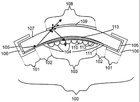
Figure 1 is a cross-sectional side view of a light fixture in accordance with
one
embodiment of this invention.
Figure 2 is a cross-sectional side-view of the lightguide of Figure 1
Figure 3 is a top view of the lightguide of Figure 1.
Figure 4 is a shaded perspective view of the lightguide of Figure 1.
Figure 5 is a chart depicting the measurements of the angular far-field
luminous
intensity of the output from a light fixture of one embodiment of this
invention with different
volumetric light scattering films.
Figure 6 is a chart depicting the measurements of the angular far-field
luminous
intensity of the output from a light fixture of one embodiment of this
invention with different
volumetric light scattering films and a light redirecting element.
Figure 7 is a cross-sectional side view of the light redirecting element of
Figure 1.
Figure 8 is a photometric report of the output from a light fixture of one
embodiment of
this invention.
Figure 9 is a cross-sectional side view of a single edge-lit indirect light
fixture in
accordance with one embodiment of this invention.
Figure 10 is a cross-sectional side view of a single edge-lit direct light
fixture in
3o accordance with one embodiment of this invention.
Figure 11 is a cross-sectional side view of a single edge-lit direct/indirect
light fixture
in accordance with one embodiment of this invention.
-3-
CA 02702690 2010-05-03
Figure 12 is a photometric report of the output from a light fixture of the
type shown in
FIG. 11.
Figure 13 is a cross-sectional side view of a single edge-lit direct light
fixture oriented
vertically in accordance with one embodiment of this invention.
Figure 14 is an underside view of a double edge-lit light fixture comprising a
rectangular light emitting region in accordance with one embodiment of this
invention.
Figure 15 is an underside view of a double edge-lit light fixture comprising a
wave-like
shaped light emitting region in accordance with one embodiment of this
invention.
Figure 16 is an underside view of a double edge-lit light fixture comprising
1o substantially circular light emitting regions in accordance with one
embodiment of this
invention.
Figure 17 is an underside view of a quadruple edge-lit light fixture
comprising a
rectangular non-scattering region enclosed by a rectangular light emitting
region wherein any
point on the light emitting region is disposed between two non-scattering
regions in accordance
with one embodiment of this invention.
Figure 18 is an underside view of a quadruple edge-lit light fixture
comprising a
circular non-scattering region enclosed by a circular light emitting region
wherein any point on
the light emitting region is disposed between two non-scattering regions in
accordance with
one embodiment of this invention.
Figure 19 is an underside view of a circularly illuminated edge-lit light
fixture
comprising a non-scattering region disposed between the LEDs and a circular
light emitting
region in accordance with one embodiment of this invention.
Figure 20 is an cross-sectional side view of an edge-lit indirect light
fixture wherein the
LEDs are disposed in a central region with their optical axis directed away
from the central
region and a non-scattering region is disposed between a light blocking region
and a light
emitting region in accordance with one embodiment of this invention.
Figure 21 is an cross-sectional side view of an edge-lit direct/indirect light
fixture
wherein the LEDs are disposed in a central region with their optical axis
directed away from
the central region and a non-scattering region is disposed between a light
blocking region and a
light emitting region in accordance with one embodiment of this invention.
Figure 22 is a depiction of four edge-lit light fixtures comprising a square
light emitting
region and a non-scattering region in accordance with one embodiment of this
invention.
-4-
CA 02702690 2010-05-03
Figure 23 is a computer generated rendering of two double edge-lit light
fixtures
comprising a rectangular light emitting region and a non-scattering region in
accordance with
one embodiment of this invention.
Figure 24 is a computer generated rendering of a double edge-lit light fixture
comprising multiple circular light emitting regions and a non-scattering
region in accordance
with one embodiment of this invention.
Figure 25 is a report comprising the light output profiles, photographs, areas
of the light
extracting regions and optical efficiency of single edge-lit light fixtures
comprising a 24 inch
by 24 inch lightguide wherein the light extracting region is a volumetric
light scattering
1o diffuser film with asymmetric diffusing angles of 56 x 2 with the major
axis of diffusion
oriented orthogonal the array of LEDs at an edge.
Figure 26 is a computer generated rendering of multiple edge-lit light
fixtures
comprising light emitting regions and non-scattering regions in accordance
with embodiments
of this invention.
Figure 27 is a photograph of the output from a light fixture of the type shown
in FIG.15.
Figure 28 is a report comprising the candela distribution, zonal lumen summary
and
angular light output profiles of the light fixture in FIG. 27.
Figure 29 is a computer generated rendering of a double edge-lit
direct/indirect linear
pendant light fixture of the type shown in FIG. 14 in accordance with one
embodiment of this
invention.
Figure 30 are the dimensional drawings of the light fixture of Figure 29 where
the units
are in inches in accordance with one embodiment of this invention.
Figure 31 is a computer generated rendering of two double edge-lit
direct/indirect linear
pendant light fixtures comprising lightguides curved in a convex form relative
to the nadir in
accordance with one embodiment of this invention.
Figure 32 are the dimensional drawings of the light fixture of Figure 31 where
the units
are in inches in accordance with one embodiment of this invention.
Figure 33 is a computer generated rendering of four light fixtures illuminated
from a
central recessed region of the lightguide wherein a portion of the light
emitting region is the
light blocking region in accordance with one embodiment of this invention.
Figure 34 comprises a cross-sectional, top, side, and bottom view of a light
fixture in
FIG. 33.
-5-
CA 02702690 2010-05-03
Figure 35 is a cross-sectional side view of edge-lit light fixture comprising
a lightguide
with a non-curved light input edge in accordance with one embodiment of this
invention.
Figure 36 is a cross-sectional side view of edge-lit light fixture comprising
a lightguide
with a curved light input edge in accordance with one embodiment of this
invention.
Figure 37 is a cross-sectional side view of a double edge-lit direct/indirect
light fixture
comprising a light extracting volumetric scattering element on the bottom
surface of the
lightguide depicting the increased angular width of the direct light relative
to the indirect light
in accordance with one embodiment of this invention.
Figure 38 is a cross-sectional side view of a double edge-lit direct/indirect
light fixture
1o comprising a light extracting volumetric scattering element on the top
surface of the lightguide
depicting the increased angular width of the indirect light relative to the
direct light in
accordance with one embodiment of this invention.
DETAILED DESCRIPTION OF THE INVENTION
The features and other details of the invention will now be more particularly
described
with reference to the accompanying drawings, in which embodiments of the
inventive subject
matter are shown. It will be understood that particular embodiments described
herein are
shown by way of illustration and not as limitations of the invention. However,
this inventive
subject matter should not be construed as limited to the embodiments set forth
herein. The
principal features of this invention can be employed in various embodiments
without departing
from the scope of the invention. All parts and percentages are by weight
unless otherwise
specified. All patent applications and patents referenced herein are
incorporated by reference.
The terminology used herein is for the purpose of describing particular
embodiments
only and is not intended to be limiting of the inventive subject matter. Like
numbers refer to
like elements throughout. As used herein the term "and/or" includes any and
all combinations
of one or more of the associated listed items. Also, as used herein, the
singular forms "a", "an"
and "the" are intended to include the plural forms as well, unless the context
clearly indicates
otherwise. It will be further understood that the terms "comprises" and/or
"comprising," when
used in this specification, specify the presence of stated features, integers,
steps, operations,
elements, and/or components, but do not preclude the presence or addition of
one or more other
features, integers, steps, operations, elements, components, and/or groups
thereof.
-6-
CA 02702690 2010-05-03
Definitions
For convenience, certain terms used in the specification and examples are
collected
here.
"Optically coupled" is defined herein as including the coupling, attaching or
adhering
two or more regions or layers such that the intensity of light passing from
one region to the
other is not substantially reduced due to Fresnel interfacial reflection
losses due to differences
in refractive indices between the regions. Optical coupling methods include
joining two
regions having similar refractive indices, or by using an optical adhesive
with a refractive index
substantially near or in-between at least one of the regions or layers such as
Optically Clear
1o Adhesive 8161 from 3M (with a refractive index at 633 nm of 1.474).
Examples of optically
coupling include lamination using an index-matched optical adhesive such as a
pressure
sensitive adhesive; lamination using a UV curable transparent adhesive;
coating a region or
layer onto another region or layer; extruding a region or layer onto another
region or layer; or
hot lamination using applied pressure to join two or more layers or regions
that have
substantially close refractive indices. A "substantially close" refractive
index difference is
about 0.5, 0.4, 0.3 or less, e.g., 0.2 or 0.1.
"Diffusion angle" is a measurement of the angular diffusion profile of the
intensity of
light within a plane of emitted light. Typically the diffusion angle is
defined according to an
angular Full-Width-at-Half-Maximum (FWHM) intensity defined by the total
angular width at
50% of the maximum intensity of the angular light output profile. For
diffusive films and
sheets, this is typically measured with collimated light at a specific
wavelength or white light
incident normal to the film. Typically, for anisotropic diffusers, the FWHM
values are
specified in two orthogonal planes such as the horizontal and vertical planes
orthogonal to the
plane of the film. For example, if angles of +35 and -35 were measured to
have one-half of
the maximum intensity in the horizontal direction, the FWHM diffusion angle in
the horizontal
direction for the diffuser would be 70 . Similarly, the full-width at one-
third maximum and
full-width at one-tenth maximum can be measured from the angles at which the
intensity is
one-third and one-tenth of the maximum light intensity respectively.
The "asymmetry ratio" is the FWHM diffusion angle in a first light exiting
plane
3o divided by the FWHM diffusion angle in a second light exiting plane
orthogonal to the first,
-7-
CA 02702690 2010-05-03
and thus is a measure of the degree of asymmetry between the intensity profile
in two
orthogonal planes of light exiting the diffuser.
A "spheroidal" or "symmetric" particle includes those substantially resembling
a
sphere. A spheroidal particle may contain surface incongruities and
irregularities but has a
generally circular cross-section in substantially all directions. A spheroid
is a type of ellipsoid
wherein two of the 3 axes are equal. An "asymmetric" particle is referred to
here as an
"ellipsoidal" particle wherein each of the three axis can be a different
length. Ellipsoidal
particles can range in shapes from squashed or stretched spheres to very long
filament like
shapes.
A "spherical" or "symmetric" disperse phase domain includes gaseous voids,
micro-
bodies, or particles that substantially resemble a sphere. A spherical domain
may contain
surface incongruities and irregularities but has a generally circular cross-
section in substantially
all directions. A "spheroid" is a type of ellipsoid wherein two of the three
axes are equal. An
"asymmetric" domain is referred to here as an "ellipsoidal" domain wherein
each of the three
axis can be a different length. Typically, ellipsoidal domains resemble
squashed or stretched
spheres. "Non-spherical" domains include ellipsoidal domains and other domains
defined by
shapes that do not resemble a sphere such as those that not have constant
radii. For example, a
non-spherical particle may have finger-like extensions within one plane
(amoeba-like) and
substantially planar in a perpendicular plane. Also, fibrous domains are also
non-spherical
disperse phase domains that may have aspect ratios of 10:1, 100:1 or larger.
"Light guide" or "waveguide" refers to a region bounded by the condition that
light rays
traveling at an angle that is larger than the critical angle will reflect and
remain within the
region. In a light guide, the light will reflect or TIR (totally internally
reflect) if it the angle (a)
from the surface normal does not satisfy the condition a < sin-'~n2 ) where nj
is the refractive
n,
index of the medium inside the light guide and n2 is the refractive index of
the medium outside
the light guide. Typically, n2 is air with a refractive index of nZl, however,
high and low
refractive index materials can be used to achieve light guide regions. The
light guide may
comprise reflective components such as reflective films, aluminized coatings,
surface relief
features, and other components that can re-direct or reflect light. The light
guide may also
contain non-scattering regions such as substrates. Light can be incident on a
light guide region
-8-
CA 02702690 2010-05-03
from the sides or below and surface relief features or light scattering
domains, phases or
elements within the region can direct light into larger angles such that it
totally internally
reflects into smaller angles such that the light escapes the light guide. The
light guide does not
need to be optically coupled to all of its components to be considered as a
light guide. Light
may enter from any face (or interfacial refractive index boundary) of the
waveguide region and
may totally internally reflect from the same or another refractive index
interfacial boundary. A
region can be functional as a waveguide for purposes illustrated herein as
long as the thickness
is larger than the wavelength of light of interest. For example, a light guide
may be a 5 micron
region with 2 micron x 3 micron ellipsoidal dispersed particles or it may be a
3 millimeter
1o diffuser plate with 2.5 micron x 70 micron dispersed phase particles.
A "luminophor" emits light when it becomes excited. The expression "excited"
means
that at least some electromagnetic radiation (e.g., visible light, UV light or
infrared light) is
contacting the luminophor, causing the luminophor to emit at least some light.
The expression
"excited" encompasses situations where the luminophor emits light continuously
or
intermittently at a rate such that a human eye would perceive it as emitting
light continuously,
or where a plurality of luminophors of the same color or different colors are
emitting light
intermittently and/or alternatingly (with or without overlap in "on" times) in
such a way that a
human eye would perceive them as emitting light continuously (and, in cases
where different
colors are emitted, as a mixture of those colors).
In one embodiment of this invention, a light emitting device comprises a
lightguide, a
light extracting region, and a non-scattering region. In another embodiment of
this invention,
the light emitting device further comprises a light redirecting element
disposed to receive and
redirect a first portion of light extracted from the lightguide. In a further
embodiment of this
invention, the lightguide is curved and the light redirecting element
redirects a first portion of
light from a first angular range from the normal to the light output surface
of the light emitting
device to a second light output angular range from the normal to the light
output surface
wherein the second light output angular range is smaller than the first
angular range. In a
further embodiment of this invention, the light emitting device further
comprises a light
blocking region and a substantially non-scattering light transmitting region.
In a further
3o embodiment of this invention, the light extracting region is a volumetric
light scattering
element optically coupled in a first region to the lightguide. In another
embodiment of this
invention, the volumetric light scattering material has a angular full-width
at half -maximum
-9-
CA 02702690 2010-05-03
intensity when illuminated with collimated incident light in a first output
plane of at least 5 . In
some embodiments, the volumetric light scattering material has a angular full-
width at half-
maximum intensity when illuminated with collimated incident light in a first
output plane of
one selected from the group of 0 to 10 , 10 to 20 , 20 to 30 , 30 to 40 ,
40 to 50 , 50 to
60 , 60 to 70 , 70 to 80 , 80 to 90 , and 90 to 100 . 0 to 10 , 10 to 20
, 20 to 30 , 30 to
40 , 40 to 50 , 50 to 60 , 60 to 70 , 70 to 80 , 80 to 90 , and 90 to
100 . In one
embodiment of this invention, the volumetric light scattering material
symmetrically scatters
incident light such that the angular FWHM in a first light output plane is
substantially the same
as the angular FWHM in a second light output plane orthogonal to the first
light output plane.
1o In another embodiment of this invention, the volumetric light scattering
material
asymmetrically scatters incident light such that the asymmetry ratio is
greater than 1.05.
LIGHT SOURCE
In one embodiment of this invention, the light emitting device comprises at
least one
light source selected from the group of: fluorescent lamp, cylindrical cold-
cathode fluorescent
lamp, flat fluorescent lamp, light emitting diode, organic light emitting
diode, field emissive
lamp, gas discharge lamp, neon lamp, filament lamp, incandescent lamp,
electroluminescent
lamp, radiofluorescent lamp, halogen lamp, incandescent lamp, mercury vapor
lamp, sodium
vapor lamp, high pressure sodium lamp, metal halide lamp, tungsten lamp,
carbon arc lamp,
electroluminescent lamp, laser, photonic bandgap based light source, quantum
dot based light
source and other solid state light emitters including inorganic and organic
light emitters.
Examples of types of such light emitters include a wide variety of light
emitting diodes
(inorganic or organic, including polymer light emitting diodes (PLEDs)), laser
diodes, thin film
electroluminescent devices, light emitting polymers (LEPs), a variety of each
of which are
well-known in the art. In one embodiment of this invention, the light source
is a transparent
OLED such as those produced by Universal Display Corporation. In a further
embodiment of
this invention, at least one of the light transmitting regions (or material)
comprises a phosphor
or phosphorescent material and the light source emits light capable of
exciting the phosphor.
In one embodiment of this invention, a light emitting device comprises at
least one light
source that is pulsed to two different power output levels at a sufficiently
high frequency such
that the output is perceived as constant. In a further embodiment of this
invention, a light
-10-
CA 02702690 2012-09-04
emitting device comprises at least one light source that is pulsed at a rate
higher than one
selected from 15 hertz, 30 hertz, 60 hertz, 120 hertz, 200 hertz, and 400
hertz.
MULTIPLE LIGHT SOURCES
More than one light source may be used in an array, grouping or arrangement
where the
source types, spectral output, color, angular output, output flux, spatial
locations or orientations
of the light sources may vary in one or more directions, planes or surfaces in
a predetermined,
random, quasi-random, regular or irregular manor. In one embodiment of this
invention, the
light emitting device comprises more than one light source arranged in at
least one pattern
selected from linear array, co-linear arrays, cylindrical arrays, spherical
arrays, circular array,
1o two-dimensional array, three-dimensional array, varying height array, angle
of orientation
varying array, opposing arrays oriented in substantially opposite directions
and arrays oriented
along a surface. Arrays of light sources such as LEDs can be configured as
disclosed in US
patent number 7,322,732.
In one embodiment of this invention, a light emitting device comprises an
array of light
sources disposed on at least one of a circuit board, connecting surface,
flexible connecting
surface, heat-sink, metal substrate, copper substrate, aluminum substrate,
lightguide, or
polymer substrate.
LIGHT SOURCE SPECTRAL OUTPUT
In one embodiment of this invention, a light emitting device comprises light
sources
wherein the spectral output the light source or group of sources is narrowband
or broadband.
The light source color may be a primary color, non-primary color, white, cool
white, warm
white or other color in the visible, ultraviolet, or infrared spectrum.
Various combinations of
light sources of different spectral properties may be used to provide desired
spectral output in
an angular range or spatial region or for all or a portion of the total light
output of the light
emitting device. Spectral properties of the light emitting region or the light
emitted from the
light emitting device may include overlapping first and second spectral
properties
(corresponding to first and second colors, respectively), such that a third
color is perceived with
third spectral properties. The overlap may occur spatially, such as in the
case of a red and blue
3o LED illuminating the same region of a diffuser that appears purple. Also,
the overlap may
occur in time such as a red and blue LED flashed sufficiently fast that the
perceived color is
-11-
CA 02702690 2012-09-04
purple. Combinations of different spectral sources in a light emitting device
include those
discussed in US patent numbers 5,803,579 and 7,213,940.
In one embodiment of this invention, the light source emits light of a
substantially
single color (a full wavelength bandwidth at have maximum intensity of less
than 40
nanometers for example). In another embodiment of this invention, the light
emitting device
(or the light source within a light emitting device) includes a light emitting
region and a
wavelength conversion material such as a luminophor. The luminophor may be a
fluorophore,
a phosphor, or other chemical compound that manifests luminescence such as
transition metal
1o complexes (ruthenium tris-2'2'-bipyridine). In another embodiment of this
invention, a light
emitting device comprises at least one wavelength conversion material that is
a non-linear
optical material such that a first portion of incident light undergoes second
harmonic generation
(SHG), sum frequency generation (SFG), third harmonic generation (THG),
difference
frequency generation (DFG), parametric amplification, parametric oscillation,
parametric
generation, spontaneous parametric down conversion (SPDC), optical
retification, or four-wave
mixing (FWM). Examples of non-linear optical materials are known in the
photonics industry
and include potassium niobate, lithium iodate, gallium selenide. The
wavelength conversion
material may be located in or on one or more surfaces or elements within the
light emitting
device or within the light source packaging, such as a phosphor material
deposited on or in a
light scattering lens of a light emitting device or deposited near the die of
an LED or within the
LED package. Alternatively, the wavelength conversion material may be located
remotely or
outside the light source packaging, as in the case of some remote phosphors
and phosphor
films.
LIGHTGUIDE
In one embodiment of this invention, a lightguide comprises a light extracting
region.
A lightguide is a region bounded by the condition that light rays traveling at
an angle that is
larger than the critical angle will reflect and remain within the region.
Thus, a lightguide
region of a material or materials is capable of supporting a significant
number of multiple
internal reflections of light due to the refractive index difference between
the material and the
surrounding material. Typically, a lightguide or waveguide is comprised of a
polymer or glass
and the surrounding material is air or a cladding material with a lower
refractive index. A
-12-
CA 02702690 2012-09-04
lightguide may be formed from a light transmitting material. The lightguide
may contain
materials or regions within the volume that will scatter, reflect, refract, or
absorb re-emit a first
portion of light into an angular condition such that it escapes the
lightguide. In one
embodiment of this invention, a lightguide comprises a substantially
transparent, non-scattering
polymer optically coupled to a light scattering material in one or more
regions. The light
scattering material can be a volumetric scattering region or film, a surface
relief region or film,
or a combination thereof. In another embodiment of this invention, the
lightguide is a film or
sheet comprising a matrix material and light scattering domains dispersed
substantially
throughout the film or sheet. In another embodiment of this invention, the
lightguide
comprises a substantially non-scattering region and a volumetric light
scattering region, or
other combination of regions as discussed in US patent numbers 7,431,489,
7,278,785,
6,924,014, 6,379,016, 5,237,641, and 5,594,830. In one embodiment of this
invention, a light
emitting device comprises a "hollow lightguide". Examples of "hollow
lightguides" are
discussed in US Patent Number 6,481,882. In another embodiment of this
invention, a light
emitting device comprises a fluted lightguide. Examples of fluted lightguides
are discussed
in US Patent Number 6,481,882. In another embodiment of this invention, a
light emitting
device comprises a lightguide with grooves or surface relief structures on at
least one surface.
Examples of surface relief structures including grooves on lightguides are
discussed in US
Patent Number 7,046,905. Other types of lightguides are known in the
backlighting industry
and optical fiber industries.
Typically, a lightguide extends longer in a first direction than a second
direction
orthogonal to the first. In these cases and in the notation used herein, the
length, L, is the
dimension of the lightguide in the first direction and width, W, is the length
of the dimension of
the lightguide in the second direction orthogonal to the first. A lightguide
can have any desired
length or width. In some embodiments, a lightguide has a width of at least
about 0.5 inches. In
some embodiments, a lightguide has a width of at least about 1 inch or at
least about 5 inches.
A lightguide in some embodiments, has a length of at least about 1 inch. In
some
embodiments, a lightguide has a length of at least about 12 inches, at least
about 24 inches, at
least about 36 inches or at least about 48 inches. In some embodiments, a
lightguide is a
-13-
CA 02702690 2010-05-03
square, rectangular or other polygonal panel. In some embodiments, a
lightguide is a planar
panel or a curved panel.
The light may enter the lightguide through any number or combination of
surfaces of
the lightguide. Light may enter through the edge (edge-surface), larger
surface, or through a
light coupling element optically coupled to one or more surfaces of the
lightguide.
LIGHTGUIDE SHAPE
The lightguide of one embodiment of this invention is substantially planar in
shape. In
another embodiment of this invention the lightguide is substantially curved
along at least one
direction. A curved lightguide includes lightguides wherein one or more
surfaces has a surface
1o normal wherein the surface normal changes angle as one moves along the
surface in a first
direction. These can include continuously changing surfaces or curves as well
as discretely
changing (sharp corners) transitions. The lightguide may be curved on two or
more opposite
faces or only on one face. The curved shape or surface includes those that can
be defined by a
mathematical relationships such as f(x,y,z). The cross-sectional side view of
an curved surface
(or portion of a surface) of a lightguide may illustrate an arc in two-
dimensional form that takes
the shape of a full or partial circle, parabolic curve, conic section,
rational curve, or elliptic
curve.
In one embodiment of this invention, a light emitting device comprises a
lightguide
with a curved region and at least one substantially planar region. In one
embodiment of this
invention, the lightguide comprises substantially planar lightguide regions
disposed in-between
a light blocking region. By using planar lightguide regions near the light
sources, the
construction of the element for the light blocking region, such as a
reflector, is less costly since
they are simple folds rather than defined curves.
In one embodiment of this invention, the curvature of the lightguide redirects
a portion
of the output from a first region of the light emitting region by rotating the
angle of the exiting
light in the direction which the region of the surface from which it exited
was rotated relative to
a flat, planar surface. For example, when a planar lightguide is curved (or
angled) to a concave
lightguide relative to the nadir as illustrated in FIG. 1, a portion of the
light from the LEDs on
the left side of the lightguide which is extracted from the lightguide in the
region near the left
side of the light extracting region is rotated to larger angles from the nadir
than the output from
a similar planar lightguide. Similarly, a portion of the light from the LEDs
on the right side of
-14-
CA 02702690 2010-05-03
the lightguide which is extracted from the lightguide in the region near the
right side of the
light extracting region is rotated to larger angles from the nadir than the
output from a similar
planar lightguide.
When a planar lightguide is curved or angled to a convex lightguide relative
to the
nadir, a portion of the light extracted from the lightguide from the LEDs on
the left side of the
lightguide in the region near the left side of the light extracting region is
rotated to smaller
angles from the nadir than the output from a similar planar lightguide.
Similarly, a portion of
the light extracted from the lightguide from the LEDs on the right side of the
lightguide in the
region near the right side of the light extracting region is rotated to
smaller angles from the
1o nadir than the output from a similar planar lightguide.
Light traveling in a lightguide, from left to right for example, may encounter
one or
more curved boundary surfaces of the lightguide that increase or decrease the
angle of
incidence at the lightguide boundary interface relative to a planar
lightguide. In one
embodiment of this invention, the lightguide is curved or angled in a convex
shape relative to
the nadir and a portion of the angular light output of the light emitting
device relative to that of
a similar planar lightguide is directed more toward the nadir in a first plane
comprising the
curved shape. In a further embodiment of this invention, the lightguide is
curved or angled in a
concave shape relative to the nadir and a portion of the angular light output
of the light emitting
device relative to that of a similar planar lightguide is directed more away
from the nadir in a
first plane comprising the curved shape.
In a further embodiment of this invention, the light blocking region or other
element of
the light emitting device such as a housing or thermal transfer element or
heat sink reflects,
absorbs, refracts or scatters a portion of light from a light emitting region
of the light emitting
device traveling at an angle selected from 40 , 50 60 , 70 and 80 from
the nadir.
In another embodiment of this invention, the light blocking region or other
element of
the light emitting device such as a housing or thermal transfer element or
heat sink reflects,
absorbs, refracts or scatters a portion of light from a light emitting region
of the light emitting
device comprising a curved lightguide such that the luminance in an angular
region from 55
degrees to 90 degrees from the nadir is less than the luminance at the same
angle from the nadir
of a similar light emitting device with a planar, non-curved lightguide.
-15-
CA 02702690 2010-05-03
In one embodiment of this invention, a light emitting device comprises at
least one
lightguide that has a curved or polygonal cross-sectional shape in a plane
parallel to the normal
of a region of the light output surface. The lightguide may be tapered in one
or more
directions. In a further embodiment, the lightguide extends further in a first
region in a
direction parallel to a surface normal of the light emitting region or nadir
than a second region
of the lightguide. A lightguide extended further in one region than another
may include
concave cross-sections, convex cross-sections, arcuate cross-sections or other
cross sections
that are not symmetric about an axis parallel to the normal to the light
emitting output surface
or nadir in a region of the light output surface.
1o LIGHTGUIDE ORIENTATION
In one embodiment of this invention, a light emitting device comprises at
least one
lightguide oriented at a first angle alpha from one selected from the group of
light emitting
region surface normal, nadir, light output surface normal, an outer housing
surface of the light
emitting device or light fixture, optical axis of the light emitting device,
and optical axis of a
light source. In one embodiment, alpha is approximately one selected from the
group of 0 ,
30 , 45 , 60 , and 90 . In a further embodiment of this invention, alpha is
one selected from
the group of 0 < alpha < 30 , 30 < alpha < 45 , 45 < alpha < 60 , and 60 <
alpha < 90 . In a
further embodiment of this invention, a light emitting device comprises a
first lightguide
oriented at an angle alpha and a second lightguide oriented at an angle beta.
In one
embodiment, beta is approximately one selected from the group of 0 , 30 , 45 ,
60 , and 90 .
In a further embodiment of this invention, beta is one selected from the group
of 0 < beta <
, 30 < beta < 45 , 45 < beta < 60 , and 60 < beta < 90 .
LIGHTGUIDE INPUT EDGE
In one embodiment of this invention, the surface of the input edge of a
lightguide which
25 receives the light from the light source is one of curved, lens-like,
convex, concave, non-planar
or parametric surface wherein the angular orientation of the surface normal
across the surface
changes. In one embodiment of this invention, a light emitting device
comprises a lightguide
with an input surface with a concave region disposed adjacent to a light
source. A concave
surface disposed to receive light from a light source such that the light from
the light source is
30 not refracted toward the optical axis of the light source in the lightguide
will spread faster
within the lightguide in the plane of the curvature, thus reducing the mixing
distance. The
-16-
CA 02702690 2010-05-03
curvature may be in the length direction, width direction or both. In one
embodiment of this
invention, the input edge of a lightguide is concave within a first plane
parallel to the optical
axis of the light source and convex within a second plane parallel to the
optical axis of the light
source and perpendicular to the first plane. In one embodiment of this
invention, the input
surface of the lightguide is illuminated by a plurality of light sources
wherein the light from the
plurality of light sources cross paths within the lightguide. In a further
embodiment of this
invention, the lightguide comprises at least one recessed region wherein the
light output plane
or surface of the light source is at least partially disposed within the
recess.
LIGHT EMITTING REGION
In one embodiment of this invention, a light emitting device comprises a
lightguide and
a light emitting region. The light emitting region comprises the last optical
elements from
which the light leaves the light emitting device. In one embodiment of this
invention, the light
emitting region comprises at least one selected from a light scattering lens,
lightguide, light
reflecting element, reflector, housing, volumetric light scattering element,
diffuser surface
relief diffuser, optical film, substrate, substantially transparent lens or
protective or holding
cover material, and glass lens. The light emitting region may be planer,
curved, domed,
arcuate, quadric, radially symmetric, more than half of a sphere, or other
surface shape. The
light emitting region may comprise more than one lightguide in a light
emitting device and may
include a reflector or transparent, non-scattering lens or region.
LIGHT OUTPUT SURFACE
The light output surface is the outer surface of the light emitting device
comprising the
light emitting region. In one embodiment, the light output surface is the
portion of the outer
surface comprising the light emitting region where the light blocking region
is not disposed
between the light emitting region and the lightguide along a direction normal
to the light output
surface. In one embodiment of this invention, the light output surface
comprises a light
extracting region and a non-scattering region which is substantially
transparent.
LIGHT BLOCKING REGION
In one embodiment of this invention, a light emitting device comprises at
least one light
blocking region disposed between the light source and a region of the light
output surface. The
light blocking region may be a reflector, bezel, or a material with a total
luminous
transmittance 0/d of less than 50%. The light blocking region may reflect,
scatter, or absorb a
-17-
CA 02702690 2010-05-03
first portion of incident light that would not otherwise pass back into the
lightguide directly. In
one embodiment of this invention, the light blocking region is one selected
from the group of
aluminum reflector, metallic reflector, metalized film, multilayer polymeric
reflective film,
light absorbing material, and polymeric material absorbing a first portion of
light. The light
blocking material may be disposed near or on one or more surfaces of the
lightguide. In one
embodiment of this invention, the light blocking material comprises a
reflector and a light
absorbing material disposed near at least one edge of a lightguide wherein the
light absorbing
material is disposed between the reflector and the bottom surface of the
lightguide and the light
blocking region does not comprise a light absorbing material disposed on the
top surface of the
lightguide. In some embodiments, the total width of the light blocking region
ranges from
about 0.5 inches to about 100 inches in a first directions and ranges from
about 0.5 inches to
about 100 inches in a second direction normal to the first direction.
In one embodiment of this invention, the light emitting device is a direct-
indirect light
fixture and the reflector provides the mechanically coupling or physically
coupling support for
the lightguide and there is no light absorbing region between the top surface
of the lightguide
and the reflector.
REFLECTOR
In one embodiment of this invention, a light emitting device comprises a light
blocking
region comprising a reflector disposed to receive direct and indirect light
from a light source
which does not satisfy the total internal reflection condition. The reflector
may be a light
reflecting element which reflects or reflects and absorbs substantially all of
the incident light
from a light source. An example of a reflector used in a light emitting device
includes a metal
bezel or frame on a lightguide. The light source may be disposed substantially
within the
reflector and the reflector, light absorbing region or both may extend out
over a portion of one
or both faces or surfaces of a lightguide. The reflector may be a metal such
as aluminum or
aluminum composite and may be thermally coupled to the thermal transfer
element. In one
embodiment of this invention, the reflector is at least one thermal transfer
element in the light
emitting device system. Reflectors can also be composed of light transmitting
materials.
Lightguides often have reflectors near the light sources disposed near the
edge of the
lightguide to reflect light that is not coupled into the lightguide or does
not pass through the
lightguide at an angle greater than the critical angle for the lightguide. The
light reflected off
-18-
CA 02702690 2010-05-03
of the reflectors may be diffusely reflected or specularly reflected. This
reflected light may
escape the light emitting device after passing through a scattering element or
back reflector of
the light emitting device.
STRAY LIGHT NEAR LIGHT BLOCKING REGION
In one embodiment of this invention, a light emitting device comprising a
lightguide
where there is a non-scattering clear region near one or more of the light
sources and between
the end of the reflector and the light extracting element (such as a
volumetric light scattering
element), the light reflected off of a surface (top or bottom for example) of
the reflector or light
blocking region does not further diffuse and passes out through the
lightguide. This light is
often of a very high luminance due to the proximity to the light source(s).
The intensity and
orientation of the stray light emitted near a reflector is also affected by
the alignment (or
centering) of the lightguide edge with the light source or LED. When the light
source or LED
is not centered on the edge and the thickness of the edge is close to the
width of the light
emitting region of the light source, a significant portion of light may be
directly incident on the
reflector before passing through the lightguide. If the distance between the
upper and lower
faces of the reflector is larger than thickness of the lightguide disposed
between the faces, light
from a mis-aligned light source or (light source size larger than the edge
thickness) can pass
between the reflector and lightguide and emit from the device as stray light
or cause other
unwanted optical effects. In one embodiment of this invention, a light
absorbing material is
disposed in a region between the reflector and the lightguide and reduces the
intensity of stray
light and may reduce the apparent luminance of a non-scattering region.
In a further embodiment of this invention, the light blocking region comprises
a light
absorbing material disposed to receive a first portion of direct light from
the light source which
is not coupled into the lightguide or a first portion of light from the light
source which enters
the lightguide and passes out of the lightguide since it does not satisfy the
waveguide condition.
The light blocking region may be a light absorbing material that absorbs a
first portion of stray
light on at least one side of the lightguide.
LIGHT ABSORBING MATERIAL
In one embodiment of this invention, a light absorbing material is disposed in
a region
3o between the reflector and the light source such that a portion of the
incident light is absorbed.
In one embodiment of this invention, the light absorbing material has a d/8
diffuse reflectance
-19-
CA 02702690 2010-05-03
less than one selected from 90%, 70%, 50%, 30%, 20%, or 10%. The light
absorbing material
may absorb one or more visible wavelength regions more than another such that
the light which
is not absorbed has a color different than the average color of the light from
the light sources
incident on the light absorbing material. In one embodiment of this invention,
the color
difference, Au'v', between the average color of the light reaching the light
absorbing material
and the light exiting the lightguide due to reflection from the reflectors is
greater than 0.01.
In one embodiment of this invention, the light absorbing material is tinted,
dyed, or
colored black or gray and may be transmissive or opaque. The light reflecting
from the light
absorbing material or the light transmitting through the light absorbing
material may be
1o specular or diffuse and the surface of the light absorbing material may
have a high gloss or a
low gloss. A low gloss material will diffuse more light than a high gloss
material. In one
embodiment of this invention, the gloss of the light absorbing material
measured according to
the ASTM D 523 standard is less than one gloss unit selected from 80, 60, 40,
30, 20, 10 and 5.
In a further embodiment of this invention, the gloss of the light absorbing
material measured
according to the ASTM D 523 standard is greater than one gloss unit selected
from 80, 60, 40,
30, 20, 10 and 5.
The light absorbing material may be partially light absorbing and may comprise
light
transmitting materials. The light absorbing material may comprise a polymeric
material, an
organic material, inorganic material, painted surface, painted metal, or a
high temperature
material such as chlorinated PVC (CPVC) or a tinted polycarbonate or
fluoropolymer.
In one embodiment of this invention, the light absorbing material has a
luminous
transmittance measured according to ASTM D1003 less than one selected from the
group of
10%, 20%, 30%, 50%, 70% and 80%. In a further embodiment of this invention,
the light
absorbing material has reflectance less than one selected from the group of
10%, 20%, 30%,
50%, 70% and 80%. In a further embodiment of this invention, the light
absorbing material has
a luminous transmittance less than 5% and a reflectance between 0% and 20%.
NON-OPTICALLY COUPLED LIGHT BLOCKING REGION
In one embodiment of this invention, the light blocking region comprises a
light
absorbing region wherein the light absorbing region is not optically coupled
to the lightguide.
3o Light absorbing regions which are optically coupled to the lightguide can
absorb light traveling
within the lightguide in addition to the stray light which does not satisfy
the waveguide
-20-
CA 02702690 2010-05-03
condition. Light can be prevented from coupling into the light absorbing
region by using an air
gap or sufficiently low refractive index region between the light absorbing
region and the
lightguide. An air gap may be achieved in a significant portion of the
interface between the
light absorbing material and the lightguide by using a light absorbing
material with a rough
surface or low gloss.
OPTICALLY COUPLED LIGHT BLOCKING REGION
In one embodiment of this invention, the light blocking region comprises a
specularly
reflective region which is optically coupled to a region of the lightguide. A
specular reflector
which is optically coupled to a surface of a lightguide does not significantly
affect the direction
of light traveling within the lightguide. The specular reflector may be
partially absorptive or
partially transmissive or a combination of both.
LIGHT EXTRACTING REGION TYPE
In one embodiment of this invention, the light extracting region comprises the
light extracting
features and is at least one selected from the group of volumetric light
scattering region or film,
surface relief region or film, a volumetric or surface relief region or film
optically coupled in
on or more regions to the lightguide or a combination of volumetric and
surface relief light
scattering region. A light emitting device may comprise more than one or more
than one type
of light extracting region. Optical films such as volumetric light scattering
diffusers or surface
relief light scattering diffusers may be optically coupled to the lightguide
in predetermined
patterns, regions, or uniformly such that a first portion of light is
extracted from the lightguide
in the optically coupled region.
LIGHT EXTRACTING REGION LOCATION
In one embodiment of this invention, the light extracting region is disposed
within the
lightguide or on at least one surface of the lightguide. In a further
embodiment of this
invention, the light extracting region is disposed between at least one light
source and a light
output surface in a first direction parallel to the normal to the light output
surface or light
emitting region. The light emitting device of one embodiment of this invention
comprises more
than one light extracting region. On or more of the light extracting regions
may be located
within or adhered to the lightguide. The light extracting region may be
optically coupled to one
or more elements of the light emitting device. In one embodiment of this
invention, the light
extracting region is optically coupled to one or more components of the light
emitting device
-21-
CA 02702690 2012-09-04
using a low refractive index adhesive. In a further embodiment of this
invention, light
extracting region, such as a volumetric light scattering region, is located in
at least one of
within the waveguide, within a substrate, within a multi-region diffuser,
between the light
redirecting element and the lightguide, within a coating on a lightguide,
within a film optically
coupled to the lightguide, within an adhesive between two elements or regions
of a light
emitting device. The light extracting region may be coupled to the top,
bottom, or both top and
bottom surfaces of the light guide and may be on the opposite or the same side
as a light
redirecting element.
LIGHT EXTRACTION FEATURES ON THE LIGHTGUIDE
In one embodiment of this invention, a light emitting device comprises a
lightguide
with light extraction surface features disposed on or within at least one
inner or outer light
output surface. In one embodiment of this invention, the light extraction
features are disposed
to receive light from within the lightguide and re-direct a first portion of
the incident light to an
angle less than the critical angle at an outer surface of the lightguide.
Light extraction surface
features may include non-planar modifications or additions to a surface. An
example of adding
light extraction surface features include screenprinting translucent or light
scattering ink
features on the surface of the lightguide such as titanium dioxide or barium
sulfate or beads
dispersed in a methacrylate based ink or binder. An example of a subtractive
modification to a
surface to achieve light extraction features includes laser ablation of a PMMA
substrate to
achieve pits or ridges in a surface to scatter, reflect or refract incident
light from within the
lightguide. Other light extraction features included injection molded surface
features,
embossed features into the surface, optically coupling surface-relief films to
the lightguide,
optically coupling volumetric light scattering regions or films to the
lightguide, insert molding
optical elements or diffuser films to the lightguide, extruding or casting or
injection molding a
lightguide comprising light scattering domains within the volume, mechanically
or etching or
scribing features into the lightguide, abrading features into the lightguide,
sandblasting
features, printing features, photopolymerizing or selective polymerizing of
features into a layer
or coating and other methods known in the art of backlights for displays for
achieving light
extraction from a lightguide. In one embodiment of this invention, a
lightguide comprises a
light extracting features disclosed in US patent numbers
-22-
CA 02702690 2012-09-04
5,594,830, 5,237,341, 6,447,135, 6,347,873, 6,099,135, and 7,192,174.
LIGHT EXTRACTING REGION WIDTH
In one embodiment of this invention, the total width of the light extracting
region in a
first direction parallel to the optical axis of at least one light source is
less than one selected
from 95%, 90%, 80%, 70%, 60%, 50% and 30% of the total width of the lightguide
or light
output surface in the first direction. The total width of the light extracting
region contributes to
the uniformity of the light emitted from the light output surface. In a
further embodiment of
this invention, the total width of the light extracting region in a second
direction orthogonal to
1o the optical axis of at least one light source is less than one selected
from 95%, 90%, 80%, 70%,
60%, 50% and 30% of the total width of the lightguide or light output surface
in the second
direction. In one embodiment of this invention, the total width of the light
extracting region is
between 0.5 inches and 100 inches in a first direction and between 0.5 inches
and 100 inches in
a second direction orthogonal to the first direction. In some embodiments of
this invention, the
total width of the light extracting region is between 1 inches and 100 inches
in a first direction
and between 1 inch and 100 inches in a second direction orthogonal to the
first direction.
LIGHT EXTRACTING REGION AREA
In one embodiment of this invention, the total area of the light extracting
regions is less
than one selected from 95%, 90%, 80%, 70%, 60%, 50% and 30% of the total area
of the
lightguide or light output surface. The light emitting device or lightguide
may comprise
multiple light extracting regions disposed along one or more surfaces or
within one or more
lightguides within the light emitting device.
LIGHT EXTRACTING REGION SHAPE
In one embodiment of this invention, the cross-sectional shape of one or more
of the
light extracting regions or light output regions in a plane perpendicular to
the normal to the
output surface near the light extracting region is one selected from the group
of circular,
elliptical, square, rectangular, polygonal, amoeba-like, partially curved and
straight, a
combination of the aforementioned shapes or other closed shape. The shapes may
have a genus
greater than zero. Shapes with of a genus greater than zero include doughnut
like areas or
stretched doughnut like areas. In a further embodiment of this invention, the
cross-sectional
shape of one or more of the light extracting regions or light output regions
in a plane
-23-
CA 02702690 2010-05-03
perpendicular to the normal to the output surface near the light extracting
region substantially
encloses a non-scattering region.
LIGHT EXTRACTION REGION DISCONTINUITY
In one embodiment of this invention, a light emitting device comprises at
least one light
source, a lightguide, a first light extraction region disposed on the
lightguide and a second
region of light extraction disposed on the lightguide discontinuous with the
first light extraction
region.
NON-SCATTERING REGION
In one embodiment of this invention, a light emitting device comprises at
least one light
source, a lightguide, a light extraction region, a light blocking region, and
a substantially non-
scattering region disposed in-between the light blocking region and the light
extraction region.
A non-scattering region or substantially non-scattering region may comprise a
region with a
low amount or level of scattering. The non-scattering region may be
transparent and may
absorb a first portion of light such as in the case of a dyed lightguide. In a
further embodiment
of this invention, the light extracting region is disposed in-between the
light blocking region
and a non-scattering region. In one embodiment of this invention, the non-
scattering region
does not substantially scatter light incident externally from one side of the
lightguide traveling
through the lightguide and out the light output surface. In another embodiment
of this
invention, the non-scattering region width allows the light from more than one
light source to
mix within the lightguide such that the light from the light emitting device
from the light
emitting surface in the region near the non-scattering region has a spatial
luminance uniformity
greater than one selected from 40%, 50%, 60%, 70%, 80%, and 90%. The degree of
scattering,
or light redirection from the non-scattering region may be measured by a haze
measurement,
clarity measurement or angular width of substantially collimated light passing
through the
region.
Haze is one method for measuring the amount of wide angle scattering in non-
scattering
region. In one embodiment of this invention, the haze of the of the
substantially non-scattering
region measured according to ASTM D1003 with a BYK Gardner Hazemeter is less
than one
selected from the group of 2%, 5%, 7%, and 10%.
-24-
CA 02702690 2010-05-03
Clarity is method for measuring the narrow angle scattering of a non-
scattering element.
In one embodiment of this invention, the clarity of the of the non-scattering
region measured
with a BYK Gardner Hazemeter is greater than one of 90%, 93%, 95%, and 98%.
A measurement of the angular FWHM of collimated light passing through a
substantially non-scattering region is another method for determining the
amount of scatter in a
substantially non-scattering region. In one embodiment of this invention, a
substantially non-
scattering region has an angular FWHM intensity of collimated laser light at
532nm incident
normal to the region less than one of 5 , 3 , 2 and 1 in one or both light
output planes.
NON-SCATTERING REGION WIDTH
In one embodiment of this invention, a light emitting device comprises a
lightguide
with a non-scattering region and a light extracting region wherein the total
width of the non-
scattering region in a first direction parallel to the optical axis of at
least one light source is
greater than one selected from 5%, 10%, 20%, 30%, 40%, and 50% of the total
width of the
lightguide or light output surface in the first direction. In a further
embodiment of this
invention, the total width of the non-scattering region in a second direction
orthogonal to the
optical axis of at least one light source is greater than one selected from
5%, 10%, 20%, 30%,
40%, and 50% of the total width of the lightguide or light output surface in
the second
direction. In one embodiment of this invention, the total width of the non-
scattering region is
between 1 inch and 100 inches in a first direction and between 1 inch and 100
inches in a
second direction orthogonal to the first direction.
The non-scattering region may provide adequate distance in the direction
parallel to one
light source optical axis for the light flux from more than one light source
to mix. In one
embodiment of this invention, a light emitting device comprises at least two
light sources
disposed at one edge of a lightguide separated by a distance D, a light
blocking region, and a
lightguide comprising a non-scattering region of width W disposed between the
light blocking
region and the light extracting region. In a further embodiment of this
invention, ratio of W/D
is greater than one selected from 1, 1.4, 1.8, 2, 4, and 6. In a further
embodiment of this
invention, a light emitting device comprises an array of LEDs disposed at one
edge, a light
blocking region, and a transparent non-scattering region disposed between the
light blocking
3o region and the light extracting region wherein the pitch of the LEDs is
between 0.1 and 13
inches, the width of the transparent non-scattering region is between I and 25
inches and the
-25-
CA 02702690 2012-09-04
width of the light extracting region is between 3 and 100 inches in a first
direction parallel to
the optical axis of at least one light source.
VOLUMETRIC LIGHT-SCATTERING REGION OR ELEMENT
In one embodiment of this invention, the light emitting device comprises one
or more
volumetric light scattering regions, layers or elements comprising dispersed
phase domains or
voids. Volumetric or surface relief light scattering elements can be composed
of light
transmitting materials. The matrix or dispersed phase domains may be a gaseous
material
(hollow lightguide or voided diffuser, respectively, for example) or a light
transmitting
material. The volumetric or surface relief light scattering regions of one or
more embodiments
of this invention may scatter light isotropically or anisotropically. In one
embodiment of this
invention, a lightguide comprises a diffusing film comprising dispersed phase
domains within a
polymer matrix. Processing and choice of materials can create non-spherical
domains which
will scatter light anisotropically. Other methods for creating volumetric
diffusing elements or
diffusers including symmetric and asymmetric shaped domains are described in
US patent
numbers 5,932,342, 6,346,311, 6,940,643, 6,673,275, 6,567,215 and 6,917,396.
Multi-region
diffusers may also be used.
Haze is one method for measuring the amount of wide angle scattering in an
element.
In one embodiment of this invention, the haze of the of the surface relief or
volumetric light
scattering element measured according to ASTM D 1003 with a BYK Gardner
Hazemeter is
greater than one of 5%, 10%, 20%, 50%, 80%, 90%, or 99%.
Clarity is method for measuring the narrow angle scattering of a light
scattering
element. In one embodiment of this invention, the clarity of the of the
surface relief or
volumetric light scattering element measured with a BYK Gardner Hazemeter is
less than one
of 5%, 10%, 20%, 50%, 80%, 90%, or 99%.
The total luminous transmittance in the 0/d geometry of a light scattering
element or
light transmitting material is one method for measuring the forward scattering
efficiency in an
element. In one embodiment of this invention, the transmittance of the of the
surface relief or
volumetric light scattering element measured according to ASTM D1003 with a
BYK Gardner
Hazemeter is greater than one of 5%, 10%, 20%, 50%, 80%, 90%, or 99%.
-26-
CA 02702690 2010-05-03
In one embodiment of this invention, the total luminous transmittance in the
0/d
geometry of the light scattering element is greater than 85%, the haze is
greater than 90% and
the clarity is less than 15%.
Table 1 describes the angular FHWM diffusion angles in two orthogonal output
planes
(TD plane and MD plane), the percent luminous transmittance, the percent haze,
and the
percent clarity for several different volumetric light scattering films used
in embodiments of
this invention.
TDFWHM MDFWHM
% Transmission % Haze % Clarity (0) (0)
ADF1010 91 75 21.6 10 10
ADF2020 93 97 11.0 20 20
ADF3535 90 99 3.2 30 30
ADF5050 91 100 2.8 50 50
ADF6060 89 100 1.9 60 60
Table 1.
In one embodiment of this invention, a light emitting device comprises a
volumetric
scattering film optically coupled to the lightguide wherein the amount of
diffusion for the
volumetric light scattering film was chosen to achieve luminance uniformity
along a first
direction within the light emitting region of greater than one selected from
the group of 50%,
60%, 70%, 80%, and 90%. The degree of diffusion needed to achieve uniformity
depends on
many factors including the separation between the light source and the
volumetric light
scattering region, the flux of light incident in a particular region of the
volumetric light
scattering element (which is related to light output and directionality, and
positioning and
alignment of the light sources relative to the element), the method used to
couple light into the
light scattering region, and other optical parameters such as an additional
light redirecting
element that may be used.
In a further embodiment of this invention, a light emitting device comprises a
volumetric scattering film optically coupled to the lightguide wherein the
amount of diffusion
chosen for the volumetric light scattering film was chosen to achieve a
predetermined
percentage of direct and indirect light output from one or more light emitting
surfaces. In one
embodiment of this invention, the percentages of direct and indirect light
output from the light
emitting device, respectively, is selected from the group of 0% and 100%, 100%
and 0%, 0%-
-27-
CA 02702690 2012-09-04
10% and 100%-90%, 10%-20% and 90%-80%, 20%-30% and 80%-70%, 30%-40% and 70%-
60%, 40%-50% and 60%-50%, 50%-60% and 50%-40%, 60%-70% and 40%-30%, 70%-80%
and 30%-20%, 80%-90% and 20%-10%, 90%-100% and 10%-0%.
One or more of the diffusing (scattering) regions may have an asymmetric or
symmetric
diffusion profile in the forward (transmission) or backward (reflection)
directions. In one
embodiment of this invention, the light emitting device comprises more than
one volumetric
light scattering region. The scattering regions or layers may be optically
coupled or separated
by another material or an air gap. In one embodiment of this invention, the
volumetric light
scattering regions have a separation distance greater than 5 microns and less
than 300 mm. In
one embodiment of this invention, a rigid, substantially transparent material
separates two
diffusing regions. In another embodiment of this invention, the asymmetrically
diffusive
regions are aligned such that the luminance uniformity of a light emitting
device is improved.
In another embodiment, the spatial luminance profile of a light emitting
device using a linear or
grid array of light sources is made substantially uniform through the use of
one or more
asymmetrically diffusing regions.
The use of a volumetric anisotropic light scattering element or region in the
light
emitting device allows the scattering region to be optically coupled to the
light guide such that
it will still support waveguide conditions for a first portion of light. An
anisotropic surface
relief scattering region on the surface of the light guide or a surface of a
component optically
coupled to the light guide will substantially scatter light in that region out
of the light guide and
will typically not permit spatially uniform out-coupling in the case of
surface relief scattering
over a significant portion of the light guide output surface.
In one embodiment of this invention, a light emitting device comprises a
lightguide
with a volumetric anisotropic light scattering region wherein asymmetrically
shaped dispersed
phase domains of one polymer within another matrix polymer contribute to the
anisotropic light
scattering. The anisotropic scattering region may be non-polarization
dependent anisotropic
light scattering (NPDALS) or polarization dependent anisotropic light
scattering (PDALS).
Light fixtures with polarized light output can reduce the glare off of
surfaces and are discussed
in US patent number 6,297,906.
The amount of diffusion in the x-z and y-z planes for the NPDALS or PDALS
regions
affects the luminance uniformity and the angular light output profiles of the
light emitting
-28-
CA 02702690 2012-09-04
device. By increasing the amount of diffusion in one plane preferentially over
that in the other
plane, the angular light output from the light emitting device is
asymmetrically increased. For
example, with more diffusion in the x-z plane than the y-z plane, the angular
light output
(measured in the FWHM of the intensity profile) is increased in the x-z plane.
The diffusion
asymmetry introduced through one or more of the anisotropic light-scattering
regions or the
light filtering directional control element can allow for greater control over
the viewing angle,
color shift, color uniformity, luminance uniformity, and angular intensity
profile of the light
emitting device and the optical efficiency of the light emitting device. In
another embodiment,
the amount of diffusion (measured as FWHM of the angular intensity profile)
varies in the
1o plane of the diffusing layer. In another embodiment, the amount of
diffusion varies in the plane
perpendicular to the plane of the layer (z direction). In another embodiment
of this invention,
the amount of diffusion is higher in the regions in close proximity of one or
more of the light
sources.
The birefringence of one or more of the substrates, elements or dispersed
phase
domains may be greater than 0.1 such that a significant amount of polarization
selectivity
occurs due to the difference in the critical angle for different polarization
states when this
optically anisotropic material is optically coupled to or forms part of the
light guide. An
example of this polarization selectivity is found in US Patent 6,795,244.
ALIGNMENT OF MAJOR DIFFUSING AXIS IN ANISOTROPIC LIGHT SCATTERING
REGION
The alignment of the major axis of diffusion in one or more of the anisotropic
light-
scattering regions may be aligned parallel, perpendicular or at an angle 03
with respect to the
optical axis of a light source or edge of the waveguide. In one embodiment,
the axis of
stronger diffusion is aligned perpendicular to the length of a linear light
source in a cold-
cathode fluorescent edge-lit light emitting device. In another embodiment of
this invention, the
axis of stronger diffusion is aligned perpendicular to the length of a linear
array of LEDs
illuminating the edge of lightguide in an edge-lit light emitting device.
DOMAIN SHAPE
The domains within one or more light scattering regions may be fibrous,
spheroidal,
cylindrical, spherical, other non-symmetric shape, or a combination of one or
more of these
-29-
CA 02702690 2010-05-03
shapes. The shape of the domains may be engineered such that substantially
more diffusion
occurs in the x-z plane than that in the y-z plane. The shape of the domains
or domains may
vary spatially along one or more of the x, y, or z directions. The variation
may be regular,
semi-random, or random.
DOMAIN ALIGNMENT
The domains within a diffusing layer may be aligned at an angle normal,
parallel, or an
angle theta with respect to an edge of the diffusing layer or a linear light
source or array of light
sources, light source optical axis, light emitting device optical axis, or an
edge of the lightguide
or light redirecting optical element. In one embodiment, the domains in a
diffusing region are
1o substantially aligned along one axis that is parallel to a linear array of
light sources. In another
embodiment of this invention, the alignment of the dispersed phase domains
rotates from a first
direction to a second direction within the region. In one embodiment of this
invention, the light
emitting device comprises a volumetric light scattering region wherein the
domains are aligned
substantially parallel to one or more of the x direction, y direction, z
direction, or an angle
relative to the x, y, or z direction.
DOMAIN LOCATION
The domains may be contained within the volume of a continuous-phase material
or
they may be protruding (or directly beneath a partially conformable
protrusion) from the
surface of the continuous-phase material.
DOMAIN CONCENTRATION
The domains described herein in one or more light-diffusing regions may be in
a low or
high concentration. When the diffusion layer is thick, a lower concentration
of domains is
needed for an equivalent amount of diffusion. When the light-diffusing layer
is thin, a higher
concentration of domains or a greater difference in refractive index is needed
for a high amount
of scattering. The concentration of the dispersed domains may be from less
than 1% by weight
to over 50% by weight. In certain conditions, a concentration of domains
higher than 50% by
volume may be achieved by careful selection of materials and manufacturing
techniques. A
higher concentration permits a thinner diffusive layer and as a result, a
thinner light emitting
device or light filtering directional control element. The concentration may
also vary spatially
3o along one or more of the x, y, or z directions. The variation may be
regular, semi-random, or
random.
-30-
CA 02702690 2010-05-03
INDEX OF REFRACTION
The difference in refractive index between the domains and the matrix in one
or more of
the NPDALS, PDALS or other light scattering regions may be very small or large
in one or
more of the x, y, or z directions. If the refractive index difference is
small, then a higher
concentration of domains may be required to achieve sufficient diffusion in
one or more
directions. If the refractive index difference is large, then fewer domains
(lower concentration)
are typically required to achieve sufficient diffusion and luminance
uniformity. The difference
in refractive index between the domains and the matrix may be zero or larger
than zero in one
or more of the x, y, or z directions. In one embodiment of this invention, the
refractive index of
1o the domains is nPX, nry, nPZ and in the x, y, and z directions,
respectively and the refractive index
of the matrix or continuous phase region is nmX, n,,,y, nmZ in the x, y, and z
directions,
respectively, wherein at least one of InpX-n.1>0.001, Inpy-nmyl>0.001, or Inpx-
nmxl>0.001.
The refractive index of the individual polymeric domains is one factor that
contributes
to the degree of light scattering by the film. Combinations of low- and high-
refractive-index
materials result in larger diffusion angles. In cases where birefringent
materials are used, the
refractive indexes in the x, y, and z directions can each affect the amount of
diffusion or
reflection in the processed material. In some applications, one may use
specific polymers for
specific qualities such as thermal, mechanical, or low-cost; however, the
refractive index
difference between the materials (in the x, y, or z directions, or some
combination thereof) may
not be suitable to generate the desired amount of diffusion or other optical
characteristic such
as reflection. In these cases, it is known in the field to use small domains,
typically less than
100 nm in size to increase or decrease the average bulk refractive index.
Preferably, light does
not directly scatter from these added domains, and the addition of these
domains does not
substantially increase the absorption or backscatter.
During production of the light filtering directional control element or one of
its regions,
the refractive index of the domains or the matrix or both may change along one
or more axes
due to crystallization, stress- or strain-induced birefringence or other
molecular or polymer-
chain alignment technique.
Additive materials can increase or decrease the average refractive index based
on the
amount of the materials and the refractive index of the polymer to which they
are added, and
the effective refractive index of the material. Such additives can include:
aerogels, sol-gel
-31-
CA 02702690 2012-09-04
materials, silica, kaolin, alumina, fine domains of MgF2 (its index of
refraction is 1.38), SiO2
(its index of refraction is 1.46), A1F3 (its index of refraction is 1.33-
1.39), CaF2 (its index of
refraction is 1.44), LiF (its index of refraction is 1.36-1.37), NaF (its
index of refraction is 1.32-
1.34) and ThF4 (its index of refraction is 1.45-1.5) or the like can be
considered, as discussed
in U.S. Patent Number 6,773,801. Alternatively, fine domains having a high
index of
refraction, may be used such as fine particles of titania (T102) or zirconia
(ZrO2) or other
metal oxides.
Other modifications and methods of manufacturing anisotropic light scattering
regions,
and light emitting devices and configurations incorporating anisotropic light
scattering
elements are disclosed in US Patent 7,278,775. The modifications and
configurations
disclosed therein may be employed in an embodiment of this invention.
SCATTERING ELEMENT LOCATION
The light emitting device of one embodiment of this invention comprises one or
more
light scattering elements. On or more of the elements may be located within or
adhered to the
lightguide. The light scattering region may be optically coupled to one or
more elements of the
light emitting device. In one embodiment of this invention, the light
scattering element is
optically coupled to one or more components of the light emitting device using
a low refractive
index adhesive. In a further embodiment of this invention, the light
scattering element, such
as a volumetric light scattering region, is located in at least one of within
the waveguide, within
a substrate, within a multi-region diffuser, between the light redirecting
element and the
lightguide, within a coating on a lightguide, within a film optically coupled
to the lightguide,
within an adhesive between two elements or regions of a light emitting device.
The light
scattering element may be coupled to the top or bottom of the light guide and
may be on the
opposite or the same side as a light redirecting element.
In one embodiment of this invention, the light scattering element is patterned
or graded
in diffusion. Examples of patterned or graded diffusers and their patterns are
disclosed in US
patent number 6,867,927.
3o LIGHT TRANSMITTING MATERIAL COMPOSITION
-32-
CA 02702690 2010-05-03
In an embodiment of this invention, at least one of the lightguide, optical
film or
element, light extracting region, volumetric light scattering region, light
scattering element,
non-scattering region, light redirecting optical element, housing, mounting
element, comprises
a light transmitting material.
In one embodiment of this invention, the light transmitting material is a
polymer or a
polymer blend or alloy material comprising multiple polymers, glass, rubbers,
or other
materials. Each material may be a single phase or multiple phase material.
Such polymers include, but are not limited to acrylics, styrenics, olefins,
polycarbonates, polyesters, cellulosics, and the like. Specific examples
include poly(methyl
methacrylate) and copolymers thereof, polystyrene and copolymers thereof,
poly(styrene-co-
acrylonitrile), polyethylene and copolymers thereof, polypropylene and
copolymers thereof,
poly(ethylene-propylene) copolymers, poly(vinyl acetate) and copolymers
thereof, poly(vinyl
alcohol) and copolymers thereof, bisphenol-A polycarbonate and copolymers
thereof,
poly(ethylene terephthalate) and copolymers thereof; poly(ethylene 2,6-
naphthalenedicarboxylate) and copolymers thereof, polyarylates, polyamide
copolymers,
poly(vinyl chloride), cellulose acetate, cellulose acetate butyrate, cellulose
acetate propionate,
polyetherimide and copolymers thereof, polyethersulfone and copolymers
thereof, polysulfone
and copolymers thereof, and polysiloxanes.
Numerous methacrylate and acrylate resins are suitable for one or more phases
of the
present invention. The methacrylates include but are not limited to
polymethacrylates such as
poly(methyl methacrylate), poly(ethyl methacrylate), poly(propyl
methacrylate), poly(butyl
methacrylate), poly(isobutyl methacrylate), methyl methacrylate-methacrylic
acid copolymer,
methyl methacrylate-acrylate copolymers, and methyl methacrylate-styrene
copolymers (e.g.,
MS resins). Suitable methacrylic resins include poly(alkyl methacrylate)s and
copolymers
thereof. In particular embodiments, methacrylic resins include poly(methyl
methacrylate) and
copolymers thereof. The acrylates include but are not limited to poly(methyl
acrylate),
poly(ethyl acrylate), and poly(butyl acrylate), and copolymers thereof.
A variety of styrenic resins are suitable for polymeric phases of the present
invention.
Such resins include vinyl aromatic polymers, such as syndiotactic polystyrene.
Syndiotactic
vinyl aromatic polymers useful in the present invention include poly(styrene),
poly(alkyl
styrene)s, poly (aryl styrene)s, poly(styrene halide)s, poly(alkoxy styrene)s,
poly(vinyl ester
-33-
CA 02702690 2010-05-03
benzoate), poly(vinyl naphthalene), poly(vinylstyrene), and
poly(acenaphthalene), as well as
the hydrogenated polymers and mixtures or copolymers containing these
structural units.
Examples of poly(alkyl styrene)s include the isomers of the following:
poly(methyl styrene),
poly(ethyl styrene), poly(propyl styrene), and poly(butyl styrene). Examples
of poly(aryl
styrene)s include the isomers of poly(phenyl styrene). As for the poly(styrene
halide)s,
examples include the isomers of the following: poly(chlorostyrene),
poly(bromostyrene), and
poly(fluorostyrene). Examples of poly(alkoxy styrene)s include the isomers of
the following:
poly(methoxy styrene) and poly(ethoxy styrene). Among these examples, suitable
styrene resin
polymers include polystyrene, poly(p-methyl styrene), poly(m-methyl styrene),
polyp-tertiary
1o butyl styrene), poly(p-chlorostyrene), poly(m-chloro styrene), poly(p-
fluoro styrene), and
copolymers of styrene and p-methyl styrene. In particular embodiments,
styrenic resins include
polystyrene and copolymers thereof.
Particular polyester and copolyester resins are suitable for phases of the
present
invention. Such resins include poly(ethylene terephthalate) and copolymers
thereof,
poly(ethylene 2,6-naphthalenedicarboxylate) and copolymers thereof, poly(1,4-
cyclohexandimethylene terephthalate) and copolymers thereof, and copolymers of
poly(butylene terephthalate). The acid component of the resin can comprise
terephthalic acid,
isophthalic acid, 2,6-naphthalenedicarboxylic acid or a mixture of said acids.
The polyesters
and copolyesters can be modified by minor amounts of other acids or a mixture
of acids (or
equivalents esters) including, but not limited to, phthalic acid, 4,4'-
stilbene dicarboxylic acid,
2,6-naphthalenedicarboxylic acid, oxalic acid, malonic acid, succinic acid,
glutaric acid, adipic
acid, pimelic acid, suberic acid, azelaic acid, sebacic acid, 1, 1 2-
dodecanedioic acid,
dimethylmalonic acid, cis- 1,4-cyclohexanedicarboxylic acid and trans-l,4-
cyclohexanedicarboxylic acid. The glycol component of the resin can comprise
ethylene
glycol, 1,4-cyclohexanedimethanol, butylene glycol, or a mixture of said
glycols. The
copolyesters can also be modified by minor amounts of other glycols or a
mixture of glycols
including, but not limited to, 1,3-trimethylene glycol, 1,4-butanediol, 1,5-
pentanediol, 1,6-
hexanediol, 1,7-heptanediol, 1,8-octanediol, 1,9-nonanediol, 1,10-decanediol,
1,12-
dodecanediol, neopentyl glycol, 2,2,4,4-tetramethyl-1,3-cyclobutanediol,
diethylene glycol,
3o bisphenol A and hydroquinone. Suitable polyester resins include
copolyesters formed by the
reaction of a mixture of terephthalic acid and isophthalic acid or their
equivalent esters with a
mixture of 1,4-cyclohexanedimethanol and ethylene glycol. In particular
embodiments, the
-34-
CA 02702690 2010-05-03
polyester resins include copolyesters formed by the reaction of terephthalic
acid or its
equivalent ester with a mixture of 1,4-cyclohexanedimethanol and ethylene
glycol.
Certain polycarbonate and copolycarbonate resins are suitable for phases of
the present
invention. Polycarbonate resins are typically obtained by reacting a diphenol
with a carbonate
precursor by solution polymerization or melt polymerization. The diphenol is
preferably 2,2-
bis(4-hydroxyphenyl)propane (so-called "bisphenol A"), but other diphenols may
be used as
part or all of the diphenol. Examples of the other diphenol include 1, 1 -
bis(4-
hydroxyphenyl)ethane, 1,1-bis(4-hydroxyphenyl)cyclohexane, 2,2-bis(4-hydroxy-
3,5-
dimethylphenyl- )propane, 2,2-bis(4-hydroxy-3-methylphenyl)propane, bis(4-
1o hydroxyphenyl)sulfideandbis(4-hydroxyphenyl)sulfone. The polycarbonate
resin can be a resin
which comprises bisphenol A in an amount of 50 mol % or more, particularly 70
mol % or
more of the total of all the diphenols. Examples of the carbonate precursor
include phosgene,
diphenyl carbonate, bischloroformates of the above diphenols, di-p-tolyl
carbonate, phenyl-p-
tolyl carbonate, di-p-chlorophenyl carbonate and dinaphthyl carbonate.
Particularly suitable are
phosgene and diphenyl carbonate.
A number of poly(alkylene) polymers are suitable for phases of the present
invention.
Such polyalkylene polymers include polyethylene, polypropylene, polybutylene,
polyisobutylene, poly(4-methyl)pentene), copolymers thereof, chlorinated
variations thereof,
and fluorinated variations thereof.
Particular cellulosic resins are suitable for phases of the present invention.
Such resins
include cellulose acetate, cellulose acetate butyrate, cellulose acetate
propionate, cellulose
propionate, ethyl cellulose, cellulose nitrate. Cellulosic resins including a
variety of
plasticizers such as diethyl phthalate are also within the scope of the
present invention.
LIGHT TRANSMITTING MATERIAL ADDITIVES
Additives, components, blends, coatings, treatments, layers or regions may be
combined
on or within the aforementioned regions to provide additional properties to
the light
transmitting material. These may be inorganic or organic materials. They may
be chosen to
provide increased rigidity to enable support of additional films or light
emitting device
components. They may be chosen to provide increased thermal resistance so that
the plate or
film does not warp. They may be chosen to increase moisture resistance, such
that the plate
does not warp or degrade other properties when exposed to high levels of
humidity. These
-35-
CA 02702690 2010-05-03
materials may be designed to provide improved optical performance by reducing
wet-out when
in contact with other components in the light emitting device. Additives may
be used to absorb
ultra-violet radiation to increase light resistance of the product. They may
be chosen to
increase, decrease, or match the scratch resistance of other components in the
light fixture,
display, backlight, or other light emitting device. They may be chosen to
decrease the surface
or volumetric resistance of the element such as a lightguide or a region of
the element to
achieve anti-static properties.
The additives may be components of one or more layers of the optical element
or
lightguide. The additives may be coatings that are added onto a surface or
functional layers
1o that are a combined during the manufacturing process. The additives may be
dispersed
throughout the volume of a layer or coating or they could be applied to a
surface.
Adhesives such as pressure-sensitive or UV-cured adhesives may also be used
between
one or more layers to achieve optical coupling. Materials known to those in
the field of optical
films, plates, diffuser plates, films and backlights to provide optical,
thermal, mechanical,
environmental, electrical and other benefits may be used in the volume or on a
surface, coating,
or layer of the optical element or one of its regions. The adhesive layer may
also contain
symmetric, asymmetric, or a combination of symmetric and asymmetric domains in
order to
achieve desired light-scattering properties within the diffusion layer.
LIGHT TRANSMITTING MATERIAL ANTI-STATIC ADDITIVES
Anti-static monomers or inert additives may be added to one or more regions or
domains of the light transmitting material. Reactive and inert anti-static
additives are well
known and well enumerated in the literature. High temperature quaternary
amines or
conductive polymers may be used. As an anti-static agent, stearyl alcohol,
behenyl alcohol,
and other long-chain alkyl alcohols, glyceryl monostearate, pentaerythritol
monostearate, and
other fatty acid esters of polyhydric alcohols, etc., may be used. In
particular embodiments,
stearyl alcohol and behenyl alcohol are used.
LIGHT REDIRECTING ELEMENTS (LRE)
Light redirecting optical elements are optical elements that direct a first
portion of
incident light from a first angular direction into a second angular direction
different from the
-36-
CA 02702690 2010-05-03
first. Light redirecting elements can be composed of light transmitting
materials. Light
redirecting elements include diffusive or scattering elements, refracting
elements, reflecting
elements, re-emitting elements, diffractive elements, holographic elements, or
a combination of
two or more of the aforementioned elements. The elements may be grouped into
regions
spatially or the features may be hybrid components such as a refractive-TIR
fresnel lens hybrid
structure. Other light redirecting elements include collimating films such as
BEF film from 3M
Company and beaded bottom diffusers such as BS-700 light diffusing film from
Keiwa and
embossed light diffusing film UTE-22 from Wellstech Optical Company Ltd, off-
axis directing
films such as IDF film from 3M company, lenticular lens arrays, microlens
arrays, volumetric
diffusers, surface relief diffusers, voided diffusers, voided reflective films
or materials, multi-
layer reflective films such as ESR from 3M, polarization reflective films such
as DBEF from
3M, reflective polarizers, scattering polarizers, lightguides, diffractive or
holographic surface
relief diffusers or elements, holographic volumetric diffusers or elements,
microlenses, lenses,
other optical elements known in the optical industry to redirect light, or a
combination of two
or more of the aforementioned elements or regions of elements.
LRE AIR-GAP
In one embodiment of this invention, the LRE is separated from the lightguide
by an
air-gap or low refractive index region. By separating the LRE from the
lightguide by an air-
gap region, the LRE does not cause additional light extraction from the
lightguide at the
interface of the air-gap region.
In another embodiment of this invention, the light redirecting element is
separated from
another optical element or lightguide within the device by standoff regions.
In one
embodiment, the longest dimension of the standoffs in a plane perpendicular to
the light
emitting device optical axis is less than one selected from 3mm, lmm, 0.5 mm,
0.2mm and
0.1 mm. In one embodiment of this invention, the standoffs are small beads or
particles
disposed in region between the LRE and the lightguide. By using beads or
particles that are
sufficiently small, mechanically coupling between the LRE and lightguide can
occur without
visible sight of the light extracting from the beaded region. In one
embodiment of this
invention, the beads or domains have an average dimensional size less than one
selected from
the group of 200 m, 100 m, 75 m, 25 m and 10 m. In a further embodiment
of this
invention, the small beads or particles are dispersed between the lightguide
and LRE such that
-37-
CA 02702690 2010-05-03
the light extracted from the lightguide due to the coupling from the beads
creates a defined or
random pattern of higher luminance regions at angles further from the light
output surface
normal.
LRE SUPPORT
The light redirecting optical element may be physically coupled to a support
substrate
to position or hold it in a predetermined location within the light emitting
device. In one
embodiment of this invention, the support substrate comprises substantially
transparent, non-
scattering or refracting regions. The substrate may be held, clamped, adhered
or otherwise
physically coupled to a second element, such as the housing or metal frame of
a light emitting
device which is further physically coupled to the lightguide. In one
embodiment of this
invention, the light redirecting element may be a microlens array or
lenticular lens array pattern
disposed on a region on the surface of a clear non-scattering light
transmitting film such as an
acrylic based film. The film may be supported at one or more edges such that a
first
transparent region of the lightguide is not visibly obscured by a physical
coupler or light
blocking region which holds the light transmitting film supporting the LRE.
LRE PHYSICALLY COUPLED TO THE LIGHTGUIDE SUPPORT
In a further embodiment of this invention, the light redirecting element is
physically
coupled to the lightguide in a first region of the lightguide and LRE. In one
embodiment, the
LRE is coupled near the peripheral edges of the LRE to the lightguide using an
automatic
liquid dispenser such as those sold by I&J Fisnar Inc and a UV curable
adhesive. In a further
embodiment of this invention, the LRE is optically coupled to the lightguide
in a first region.
Where the LRE is optically coupled to the lightguide, the light is strongly
coupled out of the
lightguide. This can be used, for example, to create a pattern or desired
appearance for the
light emitting surface.
The LRE may also be mechanically or physically coupled to the lightguide
through a
framed border or patterned region. The frame may be transparent, translucent,
opaque or
partially light transmitting. The frame may have a higher transmission for
different
wavelengths of light such that the frame is colored. In one embodiment, the
frame comprises
reflective, white, mechanically coupling regions which reflect light back into
the lightguide in
the regions where the frame is physically coupled to the lightguide. In one
embodiment of this
invention, the coupling region is at least one selected from the group of
light reflective, opaque,
-38-
CA 02702690 2010-05-03
colored, or diffuse. By using a reflective coupling region, a first portion of
the light from the
lightguide may be reflected back into the lightguide. By using an opaque
coupling region, the
light that would be strongly coupled out of the lightguide at the region is
blocked from being
visible as a high luminance region. By using a colored coupling region, the
light extracted
from the lightguide in the coupling region will be visible as a reduced
luminance colored or
tinted region. If the coupling region is diffuse, the light extracted from the
lightguide may be
visible as a reduced luminance non-colored region. In a further embodiment,
the coupling
region may be a combination of more than one of the aforementioned coupling
regions. In one
embodiment of this invention, the frame is disposed to reflect, scatter, or
absorb light received
1o from a first region comprising at least one edge of the LRE such that the
light emitted from the
first region is not directly emitted from the light emitting device.
The physical coupling can be achieved through patterned adhesive deposition
(such as
ink jet type deposition systems, screenprinting systems and other systems
suitable for
depositing adhesives in a pattern) onto the lightguide and or the light
redirecting element and
laminating them or pressing them together and curing if necessary. Other
methods for coupling
include injection molding, gluing, laser welding in specific regions,
ultrasonic welding in
specific regions, localized thermal bonding and other techniques known in the
glass and plastic
bonding field to bond materials to light transmitting materials.
LRE - EDGE OBSCURATION REGION
In a further embodiment of this invention, the light emitting device comprises
a light
obscuring region disposed to scatter backwards (reflectively scatter), scatter
forward
(transmissively scatter), absorb, refract or otherwise redirect a first
portion of light from a first
region comprising at least one edge of the LRE. In one embodiment of this
invention, the light
obscuring region is a light scattering material deposited on the light
redirecting element or
supporting sheet or other element. The light scattering material may include
reflective inks,
light scattering inks, light reflecting paint, volumetric or surface relief
scattering element or
film or other scattering material. The light scattering material may be
deposited by common
methods known in the lighting or backlight printing industries such as
screenprinting, ink jet
deposition, lamination, or other adhesion techniques. In another embodiment of
this invention,
3o a frame around a first portion of the light redirecting element physically
couples the lightguide
-39-
CA 02702690 2012-09-04
to the light redirecting element and obscures a portion of the edge of the
light redirecting
element.
LRE - LENTICULAR LENS
In one embodiment of this invention, the light redirecting element is a
lenticular lens
array surface relief structure comprise a substantially linear array of convex
refractive elements
which redirect light from a first angular range into a second angular range.
In another
embodiment of this invention, the light redirecting element is a lenticular
lens array film. As
used herein, a lenticular elements or structures include, but are not limited
to elements with
cross-sectional surface relief profiles where the cross-section structure is
hemispherical,
1o aspherical, conical, triangular, rectangular, polygonal, or in the form of
an arc or other
parametrically defined curve or polygon or combination thereof. Lenticular
structures may be
linear arrays, two-dimension arrays such as a microlens array, close-packed
hexagonal or other
two-dimensional array. The features may employ refraction along with total
internal reflection
such that the output angular range is less than the input angular range within
one or more light
output planes. Lenticular structures may also be used to redirect light to an
angle substantially
off-axis from the optical axis of the element. As used herein, lenticular may
refer to any shape
of element which refracts or reflects light through total internal reflection
and includes
elements referred to as "non-lenticular" in US Patent 6,317,263. The
lenticular structure may
be disposed on a supporting substrate. In one embodiment, the focal point of
the structures is
substantially near the opposite surface of the supporting substrate. The
material, methods of
making and structures of lenticular lens arrays, microlens arrays, prismatic
films, etc. are
known in the art of light fixtures, backlights, projection screens and
lenticular and 3D
imaging.
In another embodiment of this invention, the LRE comprises a layer of beads.
Analogous to the lenticular lens array, an array comprising a randomized
assortment of beads
may be used to collimate or substantially reduce the angular extent of light
exiting from a light
transmitting lightguide. The primary differences include the fact that the
bead type light
redirecting element will reduce the angular extent of the output light in all
planes of the output
light normal to the exiting surface. However, the ability to achieve very high
levels of
collimation is limited and the fill-factor, and ultimate collimation ability
is limited due to the
-40-
CA 02702690 2010-05-03
cross-sectional area limitations of close-packing an array of spheres (or
hemispheres or
spheroidal lens-like structures).
Common materials such as those used to manufacture lenticular screens such as
vinyl,
APET, PETG, or other materials described in patents referenced elsewhere
herein may be used
in the present invention for a light transmitting material or light
redirecting element. Light
redirecting elements may comprise light transmitting materials. In a further
embodiment, a
material capable of surviving temperature exposures higher than 85 degrees
Celsius may used
as the lenticular lens or substrate to the lenticular lens or bead based
element such as biaxially
oriented PET or polycarbonate. By using a material capable of withstanding
high temperature
1o exposure, manufacturing processes such as heating during a pressure
application stage or
heating during an exposure stage may be used to decrease the production time.
In one embodiment of this invention a light emitting device comprises a
lenticular light
redirecting element that collimates light such as a 90 degree apex angle
prismatic film. In one
embodiment of this invention, a light emitting device comprises a light
redirecting element that
is a collimating film selected from the group of BEF, BEF II, BEF III, TBEF,
BEF-RP, BEFII
90/24, BEF 11 90/50, DBEF-MF1-650, DBEF-MF2-470, BEFRP2-RC, TBEF2 T 62i 90/24,
TBEF2 M 65i 90/24, NBEF, NBEF M, Thick RBEF, WBEF-520, WBEF-818, OLF-KR-1, and
3637T OLF Transport sold by 3M, PORTGRAM V7 sold by Dai Nippon Printing Co.,
Ltd.,
LUMTHRU that sold by Sumitomo Chemical Co., Ltd., ESTINAWAVE W518 and W425 DI
sold by Sekisui Chemical Co., Ltd, and RCF90 collimating film sold by
Reflexite Inc.
LRE - PITCH
The pitch of the light redirecting element or lenticular lens structure may
have an effect
on the focusing power, the thickness of the lenticular lens array and
substrate and other optical
properties such as moire. The pitch may of the LRE may be designed such that
luminance
variances due to the structures of the LRE are discernable, barely discernable
or not discernable
to a viewer at a defined distance with average visual acuity. In one
embodiment of this
invention, the pitch of the LRE is less than one selected from the group of
300 m, 200 m,
100 m or 50 m. In another embodiment of this invention, the pitch of the LRE
is greater
than or equal to one selected from the group of 100 m, 150 m, 200 m, 300
m, 400 m,
600 m and 800 m.
-41-
CA 02702690 2010-05-03
The pitch may also be specified by Lenses Per Inch, or LPI, as is commonly
used in the
graphic arts industry for elements such as lenticular lens film. One can
convert from lenses per
inch to pitch in m by dividing 25400 by the number of lenses per inch. In one
embodiment of
this invention, the pitch of the LRE is less than one selected from the group
of 85 LPI, 127
LPI, 254 LPI or 508 LPI. In another embodiment of this invention, the pitch of
the LRE is
greater than one selected from the group of 127 LPI, 85 LPI, 43 LPI, and 32
LPI.
LRE - LENS CURVATURE
The curvature of the light redirecting element or lenticular lens structure
will have an
effect on the angular optical properties of the light exiting the LRE and
light emitting device.
1o For spherical curvatures, the radius of curvature may be used to define the
degree of curvature.
In one embodiment of this invention, a light emitting device comprises a LRE
with a cross-
sectional surface curve substantially representing a portion of a circle with
a radius of curvature
less than or equal to one selected from the group of 500 m, 350 m, 250 m,
150 m, and 100
m. In a further embodiment of this invention, a light emitting device
comprises a LRE with
an aspherical surface structure with a cross-sectional surface curve
substantially representing a
portion of an ellipse. In one embodiment of this invention, the cross-
sectional curve of a
surface of the lens comprises a portion of an ellipse in the form
AX2+BXY+CY2+DX+EY+F=0.
Other shapes and variations on ellipses may be used such as disclosed in US
patent
number 6,795,250, the contents of which are incorporated herein by reference.
The radius of curvature and other optical properties of several linear
lenticular lens
films is shown in Table 2 where the lpi of the lenses are the manufacturers
product codes and
the other data is measured.
-42-
CA 02702690 2010-05-03
Units 1381pi 75lpi 60lpi
Radius of Curvature pm 115 210 310
Pitch m 200 335 421
Lens height (sag) m 59 80 83
Total thickness m 248 538 751
Lens to Flat Surface
Transmission % 92.9 89.4 90.4
Haze % 90.9 89.5 87.3
Clarity % 39.5 40.2 40.7
Flat to Lens Surface
Transmission % 70.9 75 87.7
Haze % 87.2 86.9 85.5
Clarity % 39.4 39.6 41.6
Table 2.
LRE - LENS SAGITTAL DEPTH
In one embodiment of this invention, the light redirecting element comprises a
surface
relief structure of volumetric light scattering element with a sagittal depth,
or sag, greater than
5 m. In some embodiments, the light redirecting element comprises a surface
relief structure
or volumetric light scattering element with a sag of at least 10 m, 15 m, 20
m or 25 m.
The sag depth of a lens element, such as a lenticule in a lenticular lens
array film, is the
distance from a flat plane at a given diameter of the lens to the furtherest
point on a concave
surface of the lens. As used herein, the diameters of the lens elements of the
light redirecting
element refer to the width of the light refracting lens at the base plane of
the lens.
Figure 7 is a cross-sectional side view of the light redirecting element of
Figure 1
showing the radius of curvature, sag, and pitch.
LRE - OPTICAL PROPERTIES
The light redirecting optical element may redirect light through optical
properties in a
region of the volume of the element, through a first surface, through a second
surface or
through a combination of volume and surfaces. When the element has different
optical
properties on two opposing surfaces, the optical properties may vary when
measured with light
incident on the first surface compared to light incident on the second
surface. This can be seen
in the data shown in Table 2 where the optical properties of haze,
transmission, and clarity for
different linear lenticular lens array films vary depending on whether the
light is incident on
lens side first (Lens to Flat) or the flat side first (Flat to Lens). The
difference can be seen
more particularly with partially collimated incident light as is the case with
the BYK Gardner
hazemeter complying with ASTM D1003 specifications. The data in Table 2
illustrates the
-43-
CA 02702690 2010-05-03
reduction in transmission of the light when the light enters the flat surface
first due to a
significant portion of the incident light totally internally reflecting from
the lens surface and
returning toward the source, thus reducing transmission and increasing
reflection.
Haze is one method for measuring the amount of wide angle redirection of light
in an
light redirecting element. In one embodiment of this invention, the haze of
the of the light
redirecting element measured in a first direction according to ASTM D 1003
with a BYK
Gardner Hazemeter is greater than one of 5%, 10%, 20%, 50%, 80%, 90%, or 99%.
In a
further embodiment of this invention, a light emitting device comprises a
light redirecting
element with a haze between 80% and 95% when measured in a first direction.
Clarity is one method for measuring the amount of narrow angle redirection of
light in a
light redirecting element. In one embodiment of this invention, the clarity of
the of the light
redirecting element measured in a first direction with a BYK Gardner Hazemeter
is less than
one of 5%, 10%,20%,50%,80%,90%, or 99%. Ina further embodiment of this
invention, a
light emitting device comprises a light redirecting element with a clarity
between 30% and 50%
when measured in a first direction.
The total luminous transmittance in the O/d geometry of a light scattering
element or
light transmitting material is one method for measuring the forward scattering
efficiency in an
element. In one embodiment of this invention, the transmittance of the light
redirecting
element measured according to ASTM D1003 with a BYK Gardner Hazemeter is at
least one
of 5%, 10%, 20%, 50%, 80%, 90%, or 99%. In a further embodiment of this
invention, a light
emitting device comprises a light redirecting element with a total luminous
transmittance in the
O/d geometry greater than 85% when measured in a first direction. In another
embodiment of
this invention, a light emitting device comprises a light redirecting element
with a total
luminous transmittance in the O/d geometry greater than 85% when measured in a
first
direction and less than 90% when measured in a second direction opposite the
first direction. In
another embodiment of this invention, a light emitting device comprises a
light redirecting
element with a total luminous transmittance in the O/d geometry greater than
85% when
measured in a first direction and less than 85% when measured in a second
direction opposite
the first direction.
-44-
CA 02702690 2010-05-03
LRE - COLLIMATION PROPERTIES
One or more surfaces or region of a surface of the light transmitting
material, lightguide
light redirecting element, light scattering element, or surface relief
scattering element may
include surface profiles that provide collimation properties. The collimation
properties may
direct light rays incident from large angles into angles closer to the normal
(smaller angles) of
at least one region of the light output surface of the light emitting device.
The features may be
in the form of a linear array of prisms, an array of pyramids, an array of
cones, an array of
hemispheres or other feature that is known to direct more light into the
direction normal to the
surface of the backlight. The array of features may be regular, irregular,
random, ordered,
1o semi-random or other arrangement where light can be collimated through
refraction, reflection,
total internal reflection, diffraction, or scattering. The degree of
collimation of light output can
be measured by looking at the luminous intensity of the light at a first angle
from the normal
compared with a second angle from the normal smaller than the first. Luminous
intensity ratios
comparing the luminous intensity at a high angle to the luminous intensity at
a lower angle is
one method for evaluating the collimation of light output or reduction of
light in higher angles.
Angles of evaluation may include the angles 0 , 30 , 40 , 50 , angles of peak
luminous
intensity, and other angles of interest such as 55 , 65 , 75 , and 85 as
detailed in American
National Standard Practice for Office Lighting, ANSI/IESNA RP-1-04 in section
9.6.2 and
other sections, the contents of which are incorporated by reference herein.
The luminous
intensity output ratios for two different angular combinations for a light
emitting device
comprising a linear lenticular lens array light redirecting element are shown
in Table 3.
LRE - LUMINOUS INTENSITY
In one embodiment of this invention, a light emitting device comprises a
lightguide and
a light redirecting element that collimates the light received from the
lightguide in a first plane
such that one or more angles of peak luminous intensity from the normal to the
light output
surface or nadir are less than the light emitting device without the light
redirecting element. In
one embodiment of this invention, the ratio of the luminous intensity at 40
from the normal to
the light output surface or nadir to the luminous intensity normal to the
light emitting surface or
at the nadir is greater than or equal to one selected from 1.2, 1.36, 1.5, 2,
2.5, 3, 4, and 5.
-45-
CA 02702690 2010-05-03
1381 i 751 i 601 i
1v(peak)/1v(00) 1.5 1.36 2
Iv(40 )/Iv(0 ) 1.5 1.36 2
Table 3
When used in certain environments, it is desirable for light fixtures to have
certain
luminous intensities at particular angles. For example, in office lighting, it
is recommended to
have luminous intensities below 300 candelas for angles greater than 55 from
the nadir to
reduce glare in environments where a majority of the occupant's time is spent
viewing visual
display terminals according to American National Standard Practice for Office
Lighting,
ANSI/IESNA RP-1-04 in section 9.6.2, the contents of which are incorporated by
reference
herein. In a further embodiment of this invention, a light emitting device
comprises at least one
light source, a lightguide, a light extracting region, a light redirecting
element, a light blocking
region, and a non-scattering region disposed on the lightguide between the
light blocking
region and the light emitting region such that the direct luminous intensity
from the light
emitting device at angles from the vertical, nadir, or normal to the light
output surface in a first
region, is less than or equal to at least one of 300 candelas at 55 , 220
candelas at 65 , 135
candelas at 75 , and 45 candelas at 85 . In a further embodiment of this
invention, the direct
luminous intensity from the light emitting device at angles from the vertical,
nadir, or normal to
the light emitting output surface in a first region, is less than or equal to
at least one of 300
candelas at 65 , 185 candelas at 75 , and 60 candelas at 85 .
DIRECT/INDIRECT LIGHT OUTPUT
In one embodiment of this invention, the light emitting device is one of a
direct light
fixture, indirect light fixture, and a direct/indirect light fixture. The
light extracted from a
lightguide may exit the lightguide from one or more surfaces. Light extracted
from a
lightguide in directions on opposite sides of a lightguide may be directed
away from the
lightguide such that the light emitting device has a direct and indirect light
output profile. The
amount of light directed in the up (indirect) or down (direct) directions from
a light emitting
device such as a light fixture can be categorized by the percentage of light
flux directed up and
directed down. In one embodiment of this invention, a light emitting device
comprising a
curved lightguide, non-scattering region, light extracting region, and light
redirecting element
has a an approximate luminous flux output selected from at least about 90% up
and up to about
-46-
CA 02702690 2010-05-03
10% down, from at least about 70% up and up to about 30% down, from at least
about 50% up
and up to about 50% down, up to about 30% up and at least about 70% down. In
another
embodiment of this invention, the luminous flux output of a light emitting
device is one
selected from 100%-90% up and 0%-10% down, 90%-70% up and 10%-30% down, 70%-
50%
up and 30%-50% down, 50%-30% up and 50%-70% down, 30%-0% up and 70%-100% down.
In a further embodiment of this invention, a light emitting device has a first
luminous flux
output in the up direction between 0% and 100% and a second luminous flux
output in the
down direction of 100% minus the first luminous flux output in the up
direction.
In a further embodiment of this invention, a light emitting device comprises a
curved
lightguide, non-scattering region, and light emitting region wherein the
device is a
direct/indirect light fixture wherein the percentages of the total luminous
output flux comprised
in the zone from 0 to 30 is 0% to 15%, 0 to 40 is 10% to 25%, 0 to 60 is
15% to 35%, 60
to 90 is 0% to 15%, 0 to 90 is 25% to 50%, and 90 to 180 is 40% to 80%.
Figure 8 shows the luminous intensity output of a direct/indirect light
fixture of one
embodiment of this invention comprising two linear arrays of LEDs illuminating
a lightguide
through opposing edges, a light blocking region disposed near the LEDs, a
light output surface
comprising a non-scattering region disposed between a light blocking region
and the light
emitting region, and a volumetric light scattering diffuser film with an
angular FWHM
intensity diffusion profile of 50 x 50 optically coupled to the lightguide
and a lenticular lens
array light redirecting film oriented with the array of lenticules parallel to
the array of LEDs
wherein the lightguide is straight (non-curved) near the LEDs and curved in-
between the
straight sections.
Factors which can affect the relative flux output upwards or downwards include
but are
not limited to lightguide shape, light extracting region properties and
orientation, location of
the light extracting region (for example top or bottom of the lightguide),
lightguide shape, light
source output profile, light source location and orientation, light
redirecting element properties,
location and orientation, and light blocking element properties, location and
orientation.
In one embodiment of this invention, a light emitting device is a direct or
indirect light
fixture comprising a lightguide and a light reflecting region disposed to
receive a first portion
of light from one surface of a lightguide and re-direct a second portion of
the first portion of
light back towards the lightguide.
-47-
CA 02702690 2010-05-03
LIGHT REFLECTING ELEMENT AND REGION
In one embodiment of this invention, a light emitting device comprises a light
reflecting
element disposed to receive light from one side of the lightguide and redirect
a first portion of
the light received back toward the lightguide. Direct-only or indirect-only
light fixtures may
comprise a light reflecting element in order to direct light that is extracted
one side of the
lightguide back through the lightguide. In one embodiment of this invention, a
light reflecting
element comprises a light reflecting region. The light reflecting region may
be specularly
reflecting, diffusely reflecting or some combination in-between. The light
reflecting region
may comprise a reflective ink, beads or other additives that substantially
reflect light of one or
more wavelength ranges. The reflective additive used in an ink or polymer
system may include
BaSO4, TiO2, organic clays, fluoropolymers, glass beads, silicone beads, cross-
linked acrylic
or polystyrene beads, alumina, or other materials known in the diffusion
screen or film industry
for backlights or projection screens such that the refractive index difference
between them and
a supporting polymer matrix or binder is sufficiently high to reflect light or
scatter light
backwards. The light reflecting region may also be a light reflecting material
such as PTFE, or
it may comprise a blend of thermoplastic polymers such as described in US
patent application
number 11/426,198, or US patent numbers 5,932,342, 5,825,543, and 5,268,225,
the text of
each is incorporated by reference herein where the refractive index between
the two polymers
is chosen to be very high such that the light reflects from the film. In
another embodiment of
this invention, the light reflecting region is a voided film such those
described in US patent
numbers 7,273,640, 5,843,578, 5,275,854, 5,672,409, 6,228,313, 6,004,664,
5,141,685, and
6,130,278, and US patent application number 10/020,404, the contents of each
are incorporated
by reference herein.
The light reflecting region may comprise nanoparticle dispersions such as
nanodispersions of aluminum or silver or other metals that can create a
specularly reflecting
ink. In one embodiment of this invention, a light emitting device comprises a
specular light
reflecting region which recycles the incident light from within the light
emitting device to
provide uniformity and the light output from the device is substantially
collimated from a light
redirecting element.
-48-
CA 02702690 2012-09-04
In one embodiment of this invention, the light reflecting region is a
multilayer dielectric
coating or a multilayer polymeric reflector film such as described in US
patent numbers
7,038,745, 6,117,530, 6,829,071, 5,825,543, and 5,867,316, or DBEF film
produced by 3M.
A multilayer polymeric reflective film can have a reflectance in the visible
spectrum greater
than 94% and thus can be more efficient in an optical system. The multi-layer
polymeric
reflector film may be specularly reflective, diffusely reflective, diffusely
transmissive,
anisotropically forward scattering or anisotropically backward scattering for
one or more
polarization states. In a light emitting device where the light reflecting
regions are a multi-
layer polymeric reflector, the low light loss enables more reflections before
the light is
absorbed and thus a cavity within the light emitting device can be made
thinner, thus
providing higher uniformity in a thinner form factor.
In one embodiment of this invention, the light reflecting element is a
symmetrically
diffusely reflecting white reflecting film such voided PET films with our
without additives such
as titanium dioxide or barium sulfate. A specularly reflecting film may also
be used such as
metallized aluminized PET film or ESR multilayer reflective film from 3M
Company or DBEF
reflective polarizer film from 3M Company. Light reflecting elements can be
composed of
light transmitting materials. In another embodiment of this invention, light
emitting device
comprises a volumetric asymmetrically reflecting element. The asymmetrically
reflecting
element may be an anisotropically backscattering volumetric diffuser, a
volumetric forward
asymmetrically scattering diffuser optically coupled to a specular reflector
or other volumetric
or surface relief based elements that reflect light anisotropically. In
another embodiment of
this invention, the reflector may be a metal such as aluminum or a metallic
compound. The
light reflecting element may be a sheet or other component or portion of the
housing that is
comprised of a light reflecting component or a metal or metallic layer or
other reflecting
component such as a polished aluminum housing. The light reflecting region may
also be a
brushed (or otherwise imparted with substantially linear features) aluminium
or a brushed,
embossed coating such that the element reflects anisotropically. In one
embodiment of this
invention, a light emitting device comprises a light reflecting element with a
d/8 diffuse
reflectance greater than one selected from 70%, 80%, 90%, or 95%. In a further
embodiment
of this invention, a light emitting device comprises an anisotropic light
reflecting element with
a d/8 diffuse reflectance greater than one selected from 70%, 80%, 90%, or
95%. In one
embodiment of this invention, a light emitting device comprises a light
reflecting film disclosed
-49-
CA 02702690 2012-09-04
in at least one of the US patent numbers 4,377,616, 4,767,675, 5,188,777,
6,497,946,
6,177,153.
LIGHT REFLECTING REGION LOCATION
In one embodiment of this invention, a light emitting device comprises a light
reflecting
region disposed on the opposite side of a lightguide from a light emitting
region. The light
reflecting region, or a portion thereof, may located on the edges of the
lightguide, the top
surface, the bottom surface, a light output surface, inbetween the light
sources, within an
optical cavity of the light emitting device, optically coupled to the
lightguide, spatially
1o separated from the lightguide, or in other regions or locations commonly
known in the lighting
industry as being suitable for reflective surfaces or regions. In one
embodiment of this
invention, light reflecting region may be separated by a distance greater than
the thickness of
the lightguide in a direction orthogonal the surface of the lightguide. By
separating the light
reflecting region from the lightguide, the light extracted from the lightguide
on the side of the
light reflecting region may travel laterally to illuminate areas of the light
reflecting region that
may reflect light through non-scattering regions of the lightguide as
illustrated in the recessed
light fixture of FIG. 22. In one embodiment of this invention, a light
emitting device comprises
a lightguide with a non-scattering region disposed between a light blocking
region and a light
extracting region, a reflective region disposed at a distance greater than the
thickness of the
lightguide from the lightguide wherein the light reflecting region extends
laterally past a first
portion of the non-scattering region of the lightguide.
ANGLE OF PEAK LUMINANCE
In one embodiment of this invention, a light emitting device comprising a
curved
lightguide and an LRE has a angular peak luminance of the light emitting
region less than one
selected from the group of 60 , 50 40 and 30 . The angular luminance peak of
the light
emitted from a lightguide comprising a volumetric scattering region can be
reduced to a lower
angle by an LRE. This can reduce direct glare or visibility of the light
emitting device when
seen from high angles from the nadir. In one embodiment of this invention, a
light emitting
device comprises a curved lightguide, a linear lenticular lens array with
radius of curvature less
than 250 m and an angular luminance peak of the central light emitting region
of the light
emitting surface less than 50 from the nadir in a plane orthogonal to the
lenticules.
-50-
CA 02702690 2010-05-03
In another embodiment of this invention, the light emitting device has a ratio
of the
peak luminance to the luminance at 0 in a first output plane greater than or
equal to one
selected from the group of 1.2, 1.5, 2, 4, 6, and 10. In another embodiment of
this invention,
the light emitting device has a ratio of the luminance at one of 40 , 55 , or
65 to the luminance
at 0 in a first output plane greater than or equal to one selected from the
group of 1.2, 1.5, 2, 4,
6, and 10.
In one embodiment, the first output plane is perpendicular to the lenticules.
The
angular luminance peak can be reduced to a lower angle by an LRE. In one
embodiment of this
invention, a light emitting device comprises a curved lightguide, a linear
lenticular lens array
with radius of curvature less than 250 tm and a luminance peak less than 50
from the nadir in
a plane orthogonal to the lenticules.
ANGULAR LUMINANCE UNIFORMITY
The angular luminance uniformity of a light emitting device is defined as
Uniformity =100%x Lmin
Lmax
where Lmax is the maximum angular luminance and Lmin is the minimum angular
luminance of a region of a the light output surface over specific angular
range. In one
embodiment of this invention, the angular luminance uniformity of the direct
light from a light
emitting region of a direct-indirect light fixtures is greater than one
selected from 40%, 50%,
60%, 70%, 80% and 90% across the angular range of 0 to 550 degrees from the
nadir or
normal to the first output surface in a first output plane.
The LRE and the curvature of the lightguide may be designed to achieve a
predetermined luminance uniformity in a first region of the light emitting
region, such as a the
center of the light emitting region, over a an angular range such as angles up
to 45 or 55 from
the nadir in a first output plane. In one embodiment of this invention, the
luminance uniformity
of the light emitting surface is greater than one selected from the group of
50%, 60%, 70%,
80% and 90% over a first luminance uniformity angular range in a first output
plane. The
luminance uniformity angular range may be from a first angle to a second angle
where the first
and second angles are selected from the group of 0 , 10 , 20 , 30 , 40 , and
50 .
-51-
CA 02702690 2010-05-03
SPATIAL LUMINANCE UNIFORMITY
The luminance and luminance uniformity of the light emitting device of one
embodiment of this invention is affected by the curve of the lightguide, the
degree of scattering
in the volumetric diffuser (the angular full width at half maximum intensity),
the light
redirecting properties of the LRE, the number, spacing and output profile of
the light sources,
and the dimensional size, shapes, and relative locations of the lightguide,
LRE, and light
sources. In one embodiment of this invention, a light redirecting element is
used to redirect
light from the lightguide and the luminance near the angle of peak luminance
falls off
significantly such that the luminance is not uniform angularly near the angle
of peak
luminance. In one embodiment of this invention, the luminance of the light
emitting region of
the light emitting device at a first angle varies from the center in direction
parallel to the array
of lenticular lens elements or lenticules. In another embodiment of this
invention, a light
emitting device comprising a curved lightguide has a light emitting region
spatial luminance
uniformity in a direction orthogonal to the array of lenticules at the angle
of peak luminance,
less than one selected from the group 80%, 70%, 60% and 50%.
The aforementioned elements affecting the luminance may also be configured to
provide spatial luminance uniformity. In another embodiment of this invention,
a light emitting
device comprising a curved lightguide has a light emitting region spatial
luminance uniformity
in a direction orthogonal to the array of lenticules at the angle of peak
luminance, greater than
one selected from the group 80%, 70%, 60% and 50%.
Figure 1 is a cross-sectional side view of a light fixture light emitting
device in
accordance with one embodiment of this invention. The following is a list of
descriptions for
the numerals represented in Figures.
100 Light emitting device
101 Light blocking region
102 Non-scattering light transmitting region
103 Light emitting region
104 Light output surface
105 Light source
106 Reflector
107 Lightguide
108 Light extracting region
109 Volumetric light scattering element
110 Light redirecting element (LRE)
111 LRE support
-52-
CA 02702690 2010-05-03
112 LRE substrate
113 Air gap
901 Indirect light (up)
902 Direct light (down)
903 Light reflecting region
EXAMPLES
A light emitting device comprises two linear arrays of light emitting diodes
wherein the
light from two linear arrays of light emitting diodes is coupled into a curved
lightguide with
1o straight segments disposed near the LEDs and substantially within a light
blocking region and
is illustrated in Figure 1. The light blocking region reflects a first portion
of light from the light
emitting diodes, provides mechanical support to the lightguide, obscures light
that does not
directly couple into the lightguide in a waveguiding condition, and provides
thermal transfer
properties to conduct heat from the LEDs. The curved lightguide has a light
output surface
comprising a light emitting region substantially centered within the light
output surface. The
area of the light emitting region is smaller than the output surface of the
lightguide and has a
non-scattering light transmitting region disposed between the light emitting
region and the light
blocking region. The light extracting region comprises a volumetric light
scattering film with a
first angular FWHM transmitted intensity in a first plane of collimated light
incident at zero
degrees. Figure 2 is a close-up side-view of the lightguide of Figure 1
further showing
dimensions and angles. Figure 3 is a top view of the lightguide of Figure 1.
Figure 4 is a
shaded perspective view of the lightguide of Figure 1.
Figure 9 illustrates a cross-sectional view of a single edge-lit indirect
light fixture
according to one embodiment of the present invention. The light fixture of
Figure 9 comprises
a reflector and a light source at least partially disposed in the reflector
and positioned to
provide light to the lightguide at a first location. In some embodiments, the
light source
comprises a plurality of light emitting diodes or other light sources operable
to provide light to
the lightguide at a plurality of locations along the edge of the lightguide.
The light fixture
comprises a volumetric light scattering element optically coupled to the
lightguide and a light
3o reflecting region in facing opposition to the volumetric light scattering
element. A
substantially non-scattering region of the lightguide is disposed between the
lightsource and the
volumetric light scattering element. In some embodiments, as discussed further
herein, the
substantially non-scattering region is at least partially visible to an
observer and forms a partial
or complete border around the volumetric light scattering element. At least a
portion of light
-53-
CA 02702690 2010-05-03
transmitted by the lightguide is extracted by the volumetric light scattering
element and emitted
upward from the light fixture as an indirect light output.
Figure 10 illustrates a cross-sectional view of a single edge-lit direct light
fixture
according to one embodiment of the present invention. In the embodiment
illustrated in Figure
10, the light reflecting region is disposed on the same side of the lightguide
as the volumetric
light scattering element. At least a portion of light transmitted by the
lightgude is extracted and
emitted downward from the light fixture as a direct light output.
Figure 11 illustrates a cross-sectional view of a single edge-lit indirect
light fixture
according to one embodiment of the present invention. The light fixture of
Figure 11
1o comprises a reflector and a light source at least partially disposed in the
reflector and
positioned to provide light to the lightguide at a first location. In some
embodiments, the light
source comprises a plurality of light emitting diodes or other light sources
operable to provide
light to the lightguide at a plurality of locations along the edge of the
lightguide. The light
fixture comprises a volumetric light scattering element optically coupled to
the lightguide. A
substantially non-scattering region of the lightguide is disposed between the
lightsource and the
volumetric light scattering element. In some embodiments, as discussed further
herein, the
substantially non-scattering region is visible to an observer and forms a
partial or complete
border around the volumetric light scattering element. At least a first
portion of light
transmitted by the lightguide is extracted by the volumetric light scattering
element and emitted
upward from the light fixture as an indirect light output, and at least a
second portion of light
transmitted by the lightguide is extracted by the volumetric light scattering
element and emitted
downward as a direct light output.
In some embodiments, an edge of a lightguide can comprise one of a variety of
shapes.
An edge of a lightguide, in some embodiments, is tapered, beveled, convex or
concave or
combinations thereof. Figure 36 is a cross-sectional side view of an edge-lit
fixture comprising
a lightguide with a curved light input edge according to one embodiment of the
present
invention. In some embodiments, an edge of a lightguide is non-curved or
straight. Figure 35
is a cross-sectional side view of an edge-lit light fixture comprising a
lightguide with a non-
curved light input edge according to one embodiment of the present invention.
Different volumetric light scattering films were optically coupled to the
lightguide and
the angular far-field luminous intensity of the output from a light fixture
comprising the
-54-
CA 02702690 2010-05-03
lightguide, two arrays of LEDs, a light blocking region and a non-scattering
region were
measured and the results are shown in Figure 5.
Figure 5 illustrates the far-field photometric profile of a light fixture
produced
comprising the components illustrated in Figure 1 except for the LRE.
Different symmetrically
scattering volumetric light scattering films were optically coupled to the
lightguide and the
angular far-field luminous intensity of the output from the light fixture in a
plane orthogonal to
the array of LEDs was measured. The different volumetric light scattering
films optically
coupled to the lightguide are a 10 x 10 angular FWHM diffuser (ADF1010), a
20 x 20
angular FWHM diffuser (ADF2020), a 35 x 35 angular FWHM diffuser (ADF3535),
and a
60 x 60 angular FWHM diffuser(ADF6060). The luminous intensity shown in
Figure 5
illustrates the affect of increasing the angular FWHM of the volumetric light
scattering film on
the light output profile. Table 2 summarizes the angular widths in degrees of
the lobes and the
angles of the peak luminous intensity extracted from the data presented in
Figure 5. In the case
of the ADF6060, there is only one lobe for the direct and one lobe for the
indirect when using
the 50% maximum criteria for the FWHM angular width. The peak angles are the
angles of
peak luminous intensity of the side lobes (in degrees) from the vertical.
Units Indirect side lobe Direct side lobe Indirect side Direct side lobe
angular width angular width lobe peak peak
ADF1010 0 50 45 123 60
ADF2020 0 45 40 125 58
ADF3535 0 53 50 133 55
ADF6060 0 130 (single lobe) 150 (single lobe) 145 48
Table 2.
In one embodiment of this invention, the FWHM angular width of the side lobes
of the
luminous intensity from the light fixture remains within an angular range of
35 to 55 . In the
fixture measured for the data for Figure 5, the peak angle of luminous
intensity associated with
the side lobes, in both the direct and indirect light output from the fixture,
moves closer to the
vertical or normal to the light output surface at the center of the fixture,
thus closer to 0 and
180 for the direct and indirect light output, respectively.
In one embodiment of this invention, a light fixture comprises at least two
light sources
illuminating two edges of a lightguide comprising a volumetric light
scattering film and a non-
-55-
CA 02702690 2010-05-03
scattering region wherein the angular peaks of the direct side lobes are
between 45 and 60
from the vertical or normal to the light output surface and the angular peaks
of the indirect side
lobes are between 120 and 150 from the vertical or normal to the light
output surface.
Different volumetric light scattering films were optically coupled to the
lightguide and
the angular far-field luminous intensity of the output from a light fixture
comprising the
lightguide, two arrays of LEDs, a light blocking region, a light redirecting
element and a non-
scattering region were measured and the results are shown in Figure 6.
Figure 6 illustrates the far-field photometric profile of a light fixture
produced
comprising the components illustrate in Figure 1 where the light redirecting
element is a
lenticular lens array with the lenticules aligned parallel to the array of
LEDs at the edges.
Different symmetrically scattering volumetric light scattering films were
optically coupled to
the lightguide and the angular far-field luminous intensity of the output from
the light fixture
was measured. The different volumetric light scattering films optically
coupled to the
lightguide range are a 10 x 10 angular FWHM diffuser (ADF1010), a 20 x 20
angular
FWHM diffuser (ADF2020), a 35 x 35 angular FWHM diffuser (ADF3535), and a 50
x 50
angular FWHM diffuser (ADF5050). Table 3 summarizes the angular widths in
degrees of the
lobes and the angles of the peak luminous intensity from the vertical
extracted from the data
presented in Figure 6. In two cases, ADF3535 and ADF5050, there is only one
lobe for the
direct and one lobe for the indirect when using the 50% maximum criteria for
the FWHM
angular width. The peak angles are the angles of peak luminous intensity of
the side lobes (in
degrees) from the vertical.
Indirect side lobe Direct side lobe Indirect Direct side Angular
FWHM angular FWHM angular side lobe lobe peak Luminanc
width width peak e
Uniformity
ADF1010 550 450 1230 450 47%
ADF2020 51 53 128 43 43%
ADF3535 140 (single lobe) 75 (single lobe) 133 38 54%
ADF5050 135 (single lobe) 70 (single lobe) 138 35 73%
Table 4.
In one embodiment of this invention, the FWHM angular width of the side lobes
of the
luminous intensity from a light fixture comprising a light redirecting element
is within a range
-56-
CA 02702690 2010-05-03
of 40 to 145 . In the fixture measured for the data for Figure 6, the peak
angle of luminous
intensity associated with the side lobes, in both the direct and indirect
light output from the
fixture with a light redirecting element, moves closer to the vertical or
normal to the light
output surface at the center of the fixture, thus closer to 0 and 180 for
the direct and indirect
light output, respectively.
In one embodiment of this invention, a light fixture comprises a light
redirecting
element and at least two light sources illuminating two edges of a lightguide
comprising a
volumetric light scattering film and a non-scattering region wherein the
angular peaks of the
direct side lobes are between 30 and 50 from the vertical or normal to the
light output surface
1o and the angular peaks of the indirect side lobes are between 120 and 150
from the vertical or
normal to the light output surface.
Also shown in Table 4, the angular luminance uniformity for the direct
illumination
portion of light output from the light fixture over the range of angles
between 0 degrees and the
peak angle of luminous intensity is higher with the larger diffusion angles of
ADF3535 and
ADF5050. In one embodiment of this invention, a light fixture comprises a
light redirecting
element and at least two light sources illuminating two edges of a lightguide
comprising a
volumetric light scattering film and a non-scattering region wherein the
angular luminance
uniformity for the direct illumination portion of light output from the light
fixture over the
range of angles between 0 degrees and the peak angle of luminous intensity is
greater than one
selected from the group of 40%, 50%, 60%, 70%, 80% and 90%.
In another aspect, the present invention provides methods of lighting a
surface. In some
embodiments, a method of lighting a surface comprises providing a light
emitting device
comprising at least one light source, a lightguide operable to receive light
from the at least one
light source at a first location on the lightguide, at least one light
extraction region optically
coupled to the lightguide, a light emitting region and a substantially non-
scattering region along
a portion of the lightguide, transmitting light from the lightsource into the
lightguide and
extracting at least a portion of light from the lightguide for emission from
the light emitting
device through the light emitting region to the surface.
In some embodiments, a method of lighting a surface comprises providing a
light
emitting device comprising at least one light source, a lightguide operable to
receive light from
the at least one light source at a first location on the lightguide, at least
one light extraction
-57-
CA 02702690 2010-05-03
region optically coupled to the lightguide, a light emitting region and a
substantially non-
scattering region along a portion of the lightguide, transmitting light from
the lightsource into
the lightguide, extracting a first portion of light from the lightguide for
emission from the light
emitting device as an indirect light output and extracting a second portion of
the light from the
lightguide for emission from the light emitting device as a direct light
output.
In some embodiments, the first portion of light is emitted from the at least
one light
extraction region. In some embodiments, the first portion of light is emitted
from the light
emitting region. In some embodiments, the second portion of light is emitted
from the at least
one light extraction region. In some embodiments, the second portion of light
is emitted from
1o the light emitting region.
EQUIVALENTS
Those skilled in the art will recognize, or be able to ascertain using no more
than
routine experimentation, numerous equivalents to the specific procedures
described herein.
Such equivalents are considered to be within the scope of the invention.
Various substitutions,
alterations, and modifications may be made to the invention without departing
from the spirit
and scope of the invention. Other aspects, advantages, and modifications are
within the scope
of the invention. The contents of all references, issued patents, and
published patent
applications cited throughout this application are hereby incorporated by
reference. The
appropriate components, processes, and methods of those patents, applications
and other
documents may be selected for the invention and embodiments thereof. The
contents of all
references, including patents and patent applications, cited throughout this
application are
hereby incorporated by reference in their entirety. The appropriate components
and methods of
those references may be selected for the invention and embodiments thereof.
Still further, the
components and methods identified in the Background section are integral to
this disclosure
and can be used in conjunction with or substituted for components and methods
described
elsewhere in the disclosure within the scope of the invention.
In describing embodiments of the invention, specific terminology is used for
the sake of
clarity. For purposes of description, each specific term is intended to at
least include all
technical and functional equivalents that operate in a similar manner to
accomplish a similar
purpose. Additionally, in some instances where a particular embodiment of the
invention
includes a plurality of system elements or method steps, those elements or
steps may be
replaced with a single element or step; likewise, a single element or step may
be replaced with
-58-
CA 02702690 2010-05-03
a plurality of elements or steps that serve the same purpose. Further, where
parameters for
various properties are specified herein for embodiments of the invention,
those parameters can
be adjusted up or down by 1/201h, 1/101h, 1/5`', 1/3rd,''A, etc, or by rounded-
off approximations
thereof, within the scope of the invention unless otherwise specified.
That which is claimed is:
-59-