Note: Descriptions are shown in the official language in which they were submitted.
CA 02702881 2010-05-11
74769-584F
1
TRANSMITTER ARCHITECTURES FOR
COMMUNICATIONS SYSTEMS
This is a divisional of Canadian National Phase Patent Application Serial
No. 2,401,891 filed March 2,2001.
BACKGROUND OF THE INVENTION
The present invention relates to electronics circuits in
communications systems, and more particularly to transmitter architectures
that
provide improved performance.
The design of a high performance transmitter is made challenging
by various design considerations. For many applications, high performance is
required to meet system specifications. High performance can be characterized
by the linearity of the transmit signal path, a wide dynamic range to control
the
transmit power, and other characteristics. Moreover, for some applications
such
as cellular communications systems, power consumption is an important
consideration because of the portable nature of the cellular telephones. Cost
is
also a major consideration for many transmitter designs that are incorporated
into mass-produced consumer products. High performance, low power
consumption, and low costs are generally conflicting design considerations.
These various design considerations effect the performance and
acceptance of many consumer products such as, for example, cellular
telephones.
Examples of cellular communications systems include Code Division Multiple
Access (CDMA), Time Division Multiple Access (TDMA), and analog frequency
modulation (FM) communications systems. CDMA communications systems are
disclosed in U.S. Patent No. 4,901,307, entitled "SPREAD SPECTRUM
MULTIPLE ACCESS COMMUNICATION SYSTEM USING SATELLITE OR
=
TERRESTRIAL REPEATERS," and U.S. Patent No. 5,103,459, entitled "SYSTEM
AND METHOD FOR GENERATING WAVEFORMS IN A CDMA CELLULAR
TELEPHONE SYSTEM," both assigned to the assignee of the present invention.
CDMA communications systems are also
defined by "TIA/EIA/IS-95-A Mobile Station-Base Station Compatibility
Standard for Dual-Mode Wideband Spread Spectrum Cellular System" and
"TIA/EIA/IS-95-B Mobile Station - Base Station Compatibility Standard for
Wideband Spread Spectrum Cellular System " .
CA 02702881 2013-01-28
74769-584F
2
In CDMA communications systems, nonlinearity in the transmitter generates
intermodulation distortion that acts as noise and degrades system performance.
To reduce
nonlinearity, the elements in the transmit signal path are designed to operate
in their linear regions
and, as the result, consume large amounts of power. Wide dynamic range is
required to adequately
control the output transmit power. In CDMA systems, the transmit power level
is adjusted to
provide the required system performance (i.e., a particular bit error rate),
low interference to other
units, and reduced power consumption. Low power consumption by the transmitter
allows for the
use of a smaller sized battery, which often translates to a smaller sized
telephone. Smaller size is
highly desirable because of the portable nature of the telephone. Low power
consumption by the
transmitter further allows for increased talk and standby times for a
specified battery size.
As can be seen, transmitter architectures that provide high performance, low
power consumption, and low costs are highly desirable.
SUMMARY OF THE INVENTION
Some embodiments of the invention may provide controller circuits that
govern the operation of transmitters for a communications system to provide
improved
performance over conventional transmitters. The improvements may include, in
some
embodiments, a combination of the following: faster response time for the
control signals,
improved linearity in the output power adjustment, reduced interference,
reduced power
consumption, lower circuit complexity, and/or lower costs. For a cellular
application, in some
embodiments, these improvements may lead to increased system capacity, smaller
telephone
size, increased talk and standby times, and/or greater public acceptance of
the products.
An aspect of the invention provides a transmitter in a communications system
that includes a variable gain element, a power amplifier section, and a
controller circuit. The
variable gain element has a variable gain covering a particular gain range.
The power
amplifier section couples to the variable gain element and includes a number
of discrete gain
settings, with one of the gain settings being a bypass setting. The controller
circuit provides
the control signals for the variable gain element and the power amplifier
section. The gains of
the variable gain element and the power amplifier section are updated in a
manner to reduce
transients in the output transmit power and to
CA 02702881 2010-05-11
74769-584F
3
provide linear adjustment of the output transmit power level. The variable
gain
element and the power amplifier section are also controlled to reduce power
consumption, e.g., by powering down one or more sections when not needed.
Another aspect of the invention provides a method and apparatus
for adjusting a gain of a circuit element in a transmitter. In accordance with
this
method and apparatus, a gain control signal that includes gain setting values
for
the circuit element is received. Overdrive pulses corresponding to changes in
the
gain setting values are then generated. The overdrive pulses are summed with
the gain setting values to generate an adjusted control signal, which is
filtered to
generate a filtered control signal. The gain of the circuit element is then
adjusted
in accordance with the filtered control signal. The overdrive pulses can have
amplitudes that are related to the magnitude of the changes in the gain
setting
values and can also have programmable duration.
Another aspect of the invention provides a method and apparatus
for adjusting signal gain in a transmitter having a first gain element and a
second
gain element. The first gain element responds to a first update clock and the
second gain element responds to a second update clock. The first and second
update clocks are asynchronous. In accordance with this method and apparatus,
the first and second gain transfer characteristics of the first and second
gain
elements, respectively, are determined. A gain compensation table is then
generated based on the first and second gain transfer characteristics. During
normal operation, first and second gain setting values for the first and
second
gain elements, respectively, are received. The second gain setting value is
adjusted with a particular gain offset value based on the first gain setting
value.
A linearized gain setting value corresponding to the adjusted second gain
setting
value is then retrieved from the gain compensation table. The gains of the
first
and second gain elements are adjusted with first and linearized gain setting
values, respectively.
Another aspect of the invention provides a method and apparatus
for adjusting signal gain in a transmitter having a first gain element and a
second
gain element. The first gain element responds to a first update clock and the
second gain element responds to a second update clock. The second update clock
is faster than the first update clock and the first and second update clocks
are
asynchronous. In accordance with the method and apparatus, the first and
CA 02702881 2010-05-11
74769-584F
4
second gain setting values are received for the first and second gain
elements,
respectively. The first and second gain control signals representative of the
first
and second gain setting values, respectively, are then generated. The first
and
second gain control signals are aligned with the first and second update
clocks,
respectively. Changes in the gain setting value of the first gain element are
detected. If a change in the gain setting value is detected, the second gain
control
signal is aligned with the first update clock; and if no change in the gain
setting
value is detected, the second gain control signal is aligned with the second
update clock. The gains of the first and second gain elements are adjusted
with
the aligned first and second gain control signals, respectively.
Another aspect of the invention provides a method and apparatus
for providing linear adjustment of output power level from a transmitter. The
transmitter includes an element having a number of discrete gain settings and
an
element having a continuously variable gain setting. In accordance with the
method and apparatus, a gain transfer function of the transmitter is
determined
for each of the discrete gain settings. For each of the discrete gain
settings, a gain
compensation table is generated based on the determined gain transfer
function.
A first gain setting value for the element having discrete gain settings is
received.
The first gain setting value identifies one of the discrete gain settings. A
second
gain setting value for the element having variable gain setting is also
received. A
compensated gain setting value is retrieved from the gain compensation table
corresponding to discrete gain setting identified by the first gain setting
value.
The gain of the element having discrete gain settings is adjusted with the
first
gain setting value, and the gain of the element having the variable gain
setting is
adjusted with the compensated gain setting value.
Another aspect of the invention provides a method and apparatus
for controlling transients in the output power of a transmitter during a
signal
transmission. The transmitter includes a first element having a first time
response and a second gain element having a second time response. The first
time response is faster than the second time response. In accordance with the
method and apparatus, first and second commands are received to adjust the
gains of the first and second elements, respectively. The first command is
delayed by a particular time period. The gains of the first and second gain
elements are adjusted with delayed first command and the second command,
CA 02702881 2014-01-21
74769-584F
respectively. The particular time period is selected to reduce increase in
output power level of
the transmitter due to adjustment of the gains of the first and second
elements. In an
embodiment, the first command is delayed when an increase in the gain of the
first element is
detected.
5 Another aspect of the invention provides a method and apparatus
for
controlling a power amplifier in a transmitter during a signal transmission.
In accordance
with the method and apparatus, the required output transmit power level is
first determined. If
the required output transmit power level is below a particular threshold, the
power amplifier is
bypassed and powered down. If the required output transmit power level exceeds
the
particular threshold, the power amplifier is powered up for at least a
particular warm up
period and then selected for use. The power amplifier can be powered down when
not in use.
The selection and bypassing/powering down of the power amplifier can be
performed at times
corresponding to boundaries of transmitted code symbols to minimize
degradation in system
performance. In a similar manner, the transmit signal path (e.g., the transmit
RF and IF
chain), as well as the biasing circuitry, can be powered down when not in use.
According to another aspect of the present invention, there is provided an
apparatus for adjusting a gain of a circuit element in a transmitter, the
apparatus comprising a
time response adjustment circuit comprising: a gain element that receives and
scales a gain
setting value for the circuit element by a scaling factor to generate a scaled
gain setting value;
a delay element that receives and delays the gain setting value by a time
delay to generate a
delayed gain setting value; and a summer that receives the scaled gain setting
value and the
delayed gain setting value and subtracts the delayed gain setting value from
the scaled gain
setting value to generate an adjusted signal; the apparatus further comprising
a modulator
coupled to the time response adjustment circuit to receive the adjusted signal
and generate a
modulator signal.
According to another aspect of the present invention, there is provided a
method for adjusting a gain of a circuit element in a transmitter, the method
comprising:
receiving and scaling, by a scaling factor, a gain setting value for the
circuit element; delaying
the gain setting value by a time delay; subtracting the delayed gain setting
value from the
CA 02702881 2014-01-21
74769-584F
5a
scaled gain setting value to generate an adjusted signal; and generating a
modulator signal
from the adjusted signal.
According to still another aspect of the present invention, there is provided
a
processor-readable memory having stored thereon instructions for execution by
a processor,
said instructions comprising code means for performing a method described
above.
The foregoing, together with other aspects of this invention, will become more
apparent when referring to the following specification, claims, and
accompanying drawings.
BRIEF DESCRIPTION OF THE DRAWINGS
FIG. 1 shows a block diagram of an embodiment of a transmitter for a
communications system;
FIG. 2 shows a block diagram of an embodiment of a transmitter that provides
advantages over the transmitter in FIG. 1;
FIG. 3 shows a block diagram of an embodiment of a controller that generates
the control signals for the transmitter in FIG. 2;
FIG. 4 shows a diagram of a portion of a gain control mechanism that includes
an embodiment of an interface circuit;
FIG. 5 shows a diagram of a specific embodiment of the interface circuit;
FIG. 6 shows a block diagram of an embodiment of a gain offset circuit;
[
CA 02702881 2010-05-11
74769-584F
5a
further comprising a modulator coupled to the time response
adjustment circuit to receive the adjusted signal and
generate a modulator signal.
According to another aspect of the present
invention, there is provided a method for adjusting a gain
of a circuit element in a transmitter, the method
comprising: receiving and scaling, by a scaling factor, a
gain setting value for the circuit element; delaying the
gain setting value by a time delay; adding the scaled gain
setting value to the delayed gain setting value to generate
an adjusted signal; and generating a modulator signal from
the adjusted signal.
The foregoing, together with other aspects of this
invention, will become more apparent when referring to the
following specification, claims, and accompanying drawings.
BRIEF DESCRIPTION OF THE DRAWINGS
FIG. 1 shows a block diagram of an embodiment of a
transmitter for a communications system;
FIG. 2 shows a block diagram of an embodiment of a
transmitter that provides advantages over the transmitter in
FIG. 1;
FIG. 3 shows a block diagram of an embodiment of a
controller that generates the control signals for the
transmitter in FIG. 2;
FIG. 4 shows a diagram of a portion of a gain
control mechanism that includes an embodiment of an
interface circuit;
FIG. 5 shows a diagram of a specific embodiment of
the interface circuit;
CA 02702881 2010-05-11
74769-584F
5b
FIG. 6 shows a block diagram of an embodiment of a
gain offset circuit;
CA 02702881 2010-05-11
74769-584F
6
FIG. 7A is a timing diagram the control signals for the driver-PA
and VGA;
FIG. 7B shows a block diagram of an embodiment for generating
the control signals for the driver-PA and VGA;
FIGS. 7C and 7D show diagrams of an embodiment of a comparator
and a logic circuit, respectively, within a timing synchronization circuit;
FIGS. 8A and 8B show diagrams of an embodiment of a high
efficiency power amplifier (HEPA) and a power amplifier circuit, respectively,
having multiple gain settings and a bypass setting;
FIG. 8C shows a diagram of an embodiment of a PA having
multiple gain settings but no bypass setting;
FIG. 9A shows a plot of a gain transfer function (or curve) of a
representative circuit element such as a VGA, driver, or PA;
FIGS. 9B and 9C are plots that show power hysteresis and power
and timing hysteresis, respectively, for a circuit element having two gain
states;
FIGS. 9D and 9E are plots that show power hysteresis and power
and liming hysteresis, respectively, for a circuit element having four gain
states;
FIGS. 10A and 10B show plots of transients in the output transmit
power due to mismatch in the response times of the driver-PA and the VGA for a
downward and an upward gain step change, respectively;
FIGS. 10C and 10D show plots of transients in the output transmit
power due to (intentionally introduced) mismatch in the time alignment of the
control signals for the driver-PA and the VGA for two different time delays;
FIG. 10E shows a diagram of an embodiment of circuitry that
delays the control signals for the driver-PA to enable control of transients
in the
output transmit power when the driver-PA gain is switched;
FIG. 11A and 11B show timing diagrams of the signals used to
control the PA and the transmit chain in accordance with an aspect of the
invention;
FIG. 11C shows a diagram of an embodiment of circuitry that
generates the control signal PA_ON to power on and off the PA; and
FIG. 11D shows a diagram of an embodiment of circuitry that
generates the control signals PA_R[1:01.
CA 02702881 2010-05-11
74769-584F
7
DESCRIPTION OF THE SPECIFIC EMBODIMENTS
Transmitter Architectures
FIG. 1 shows a block diagram of an embodiment of transmitter 100
for a communications system. The transmitter shown in FIG. 1 can be used for
various applications including cellular telephone, high definition television
(HDTV), cable television, and others. Within the transmit path, the
intermediate
frequency (IF) signal is amplified by a variable gain amplifier (VGA) 120,
upconverted to radio frequency (RF) by a mixer 122 with a sinusoidal from a
local oscillator (LO) 124, amplified by a driver 126, and buffered by a power
amplifier (PA) 128 that drives an antenna 130. Driver 126 and power amplifier
128 couple to either a high supply source (VDD_high) or a low supply source
(VDD_low), depending on the required linearity, via a switch 132 that is
controlled by a control signal PA_R1. The transmit chain of transmitter 100
includes elements in the transmit signal path (i.e., from mixer 122 to antenna
130), but not support circuitry such as local oscillator 124. The transmit
chain
includes mixer 122, driver 126, and PA 128.
In the embodiment shown in FIG. 1, PA 128 provides a fixed gain
(e.g., 29 dB) when enabled by a control signal PA_ON, and driver 126 provides
a
first gain or a second gain (e.g., 26 dB or -2 dB, respectively) depending on
the
state of the control signal PA_RO. VGA 120 provides adequate gain control to
cover the dynamic range (e.g., 85 dB) required by system specifications. A
controller 140 generates the control signals that activate PA 128, set the
gain of
driver 126, control the biasing of PA 128 and driver 126, and set the gain of
VGA
120.
Transmitter 100 is required to meet various system specifications.
For CDMA applications, the transmitter is required to operate with up to a
specified amount of nonlinearity and to provide the specified dynamic range.
Nonlinearity is reduced, in part, by providing a high power supply (VDD_high)
to
driver 126 and PA 128 at high transmit power levels and by selecting the
proper
gain (e.g., high gain) for driver 126. Although driver 126 can operate at one
of
two gain settings, the required dynamic range is provided by VGA 120 for the
reasons described below.
CA 02702881 2010-05-11
=
74769-584F
8
In the transmitter architecture shown in HG. 1, driver 126 and PA
128 are controlled by a mechanism having one update rate and VGA 120 is
controlled by another mechanism having a second update rate. Typically, the
low gain state of driver 126 is achieved by bypassing or powering down the
high
power driver stages. When driver 126 changes gain state, a gain glitch and an
undesirable and unpredictable phase shift often occur. These adverse effects
degrade the performance of the system. As a result, the gain of driver 126 is
switched at a slow rate to reduce the deleterious effects. In contrast, the
gain
control mechanism of VGA 120 has an update rate that is typically faster than
that of driver 126. The faster update rate is used to quickly adjust the gain
of the
transmit signal path in response to rapid changes in operating conditions.
In CDMA communications systems, the update dock for the driver-
PA control mechanism and the update dock for the VGA control mechanism are
locked in frequency but may not be (and are usually not) locked in phase.
Essentially, these update docks can be viewed as being asynchronous. Because
of system design considerations as described below, the update clock for the
driver-PA control mechanism is derived from a modulator of the unit in which
= the transmitter reside (e.g., the subscriber unit), and the update clock
for the VGA
control mechanism is derived from the demodulator.
The mechanism that controls driver 126 and PA 128 generally has a
faster response time than that of the mechanism that controls VGA 120. As
shown in FIG. 1, the control signals (PA_RO and PA_R1) for driver 126 and PA
128 are digital in nature and have (relatively) quick transition time. In
contrast,
the control signal VGA_GAIN for VGA 120 is filtered by a lowpass filter 142
having a particular time response T1. The bandwidth for filter 142 is designed
to
be narrow to reduce the amplitude of the ripples on the gain control signal
TX_AGC to a particular value, as required by system specifications. The narrow
bandwidth results in a (relatively) long response time (e.g., ti -a 330 sec)
for a
step change in the control signal VGA_GAIN.
For at least some of the reasons stated above (i.e., different update
rates, asynchronous update clocks, and different response times), the driver-
PA
control mechanism and the VGA control mechanism are typically designed to
operate independently from each other. However, to maintain approximately
constant output transmit power level as the gain of driver 126 is switched
from a
CA 02702881 2010-05-11
74769-584F
9
low gain setting to a high gain setting, and vice versa, the two control
mechanisms are coupled. When the gain of driver 126 is switched between gain
settings, a sudden gain step is introduced in the transmit chain that would
result
in a change in the output transmit power level. In order to compensate for
this
gain step, the gain of VGA 120 is adjusted with an offsetting gain to provide
approximately similar overall transmit signal path gain before and after
driver
126 is switched. For example, if driver 126 is switched from a gain of -2 dB
to a
gain of +26 dB, the gain of VGA is decreased by 28 dB at approximately the
same
time to compensate for the driver gain change. The response time of VGA 120
should dosely match that of driver 126. If the gain of driver 126 is switched
and
the gain of VGA 120 is not properly adjusted (i.e., because of a slow response
time), a gain transient occurs that causes a corresponding transient in the
output
transmit power. The power transient can cause degradation in the performance
of the transmitter.
FIG. 1 shows an implementation that synchronizes the two control
mechanisms to reduce gain transient when the driver is switched. Lowpass
filter
142 couples to controller 140, and receives and filters the variable control
signal
VGA_GAIN to generate analog voltages that are provided to summing amplifier
148. The control signal PA_RO for driver 126 couples to and controls a switch
144
that is coupled between a lowpass filter 146 and a summing amplifier 148.
Filter
146 couples to controller 140, and receives and filters the constant control
signal
OS_GAIN to generate a constant analog voltage that is provided to summing
amplifier 148. Amplifier 148 then sums the received voltages to generate the
VGA control signal TX_AGC.
Thus, as the gain of driver 126 is switched, a corresponding fixed
gain offset voltage (i.e., the filtered OS_GAIN) is provided to VGA 120. This
gain
offset voltage adjusts the gain of VGA 120 in the opposite direction to
maintain
an approximately constant overall transmit signal path gain. The response
times
of amplifier 148 is negligible and approximates the response time of driver
126 to
a change in the control signal PA_RO. The gain offset voltage is not added
digitally (i.e., within controller 140) before filter 142 because the response
time of
filter 142 (approximately 330 sec) is too slow relative to the fast (and
typically
negligible) response time of driver 126.
CA 02702881 2010-05-11
74769-584F
The transmitter architecture shown in FIG. 1 is suboptimal for
several reasons. First, because of the independent operation of the gain
control
mechanisms for driver 126 and VGA 120, the entire dynamic range requirement
(e.g., 85 dB) is imposed on VGA 120. This wide dynamic range requirement
5 results in a challenging and power consuming VGA design. Second, the
additional components (e.g., externally - switch 144, filter 146, and summing
amplifier 148; and internally - additional PDM for the D/A conversion of the
signal OS_GAIN) needed to maintain approximately constant output transmit
power level as driver 126 is switched increase the transmit hardware
complexity
10 and costs.
The transmitter architecture shown in FIG. 1 also fails to meet
certain system requirements. For example, TIA/EIA/IS-98-A requires the mean
output power level from the transmitter to be within 0.3 dB of the final value
in
less than 500 sec following the receipt of a valid power control bit. A wide-
bandwidth power control mechanism having fast settling time is required to
meet this specification. The processing time required to receive and determine
the validity of a power control bit can be as much as 400 sec, leaving the
transmitter with only 100 sec to respond to a detected valid power control
bit. If
the response time of filter 142 is greater than 100 sec (approximately 330
sec in
a typical design), this specification is difficult (if not improbable) to
meet.
As can be seen, various design considerations and system
requirements impose speed and accuracy requirements on the gain control
mechanism for the transmit chain.
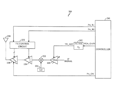
FIG. 2 shows a block diagram of an embodiment of a transmitter
200 that provides advantages over transmitter 100 in FIG. 1. Within the
transmit
path, the IF signal is amplified by a VGA 220, upconverted to RF by a mixer
222
with a sinusoidal from a local oscillator 224, amplified by a driver 226, and
buffered by a PA 228 that drives an antenna 230. Driver 226 and PA 228 couple
to a PA control circuit 232 that receives the control signals PA_RO and PA_R1
from a controller 240. The transmit chain of transmitter 200 includes VGA 220,
mixer 222, driver 226, and PA 228. PA control circuit 232 can also be
implemented within controller 240.
In the specific embodiment shown in FIG. 2, PA 228 has three gain
settings and driver 226 has two gain settings. The PA gain settings include
low
CA 02702881 2010-05-11
74769-584F
11
gain, high gain, and bypass, and the driver gain settings include low gain and
high gain. Controller 240 generates the control signals that activate PA 228,
set
the gains of driver 226 and PA 228, control the biasing of driver 226 and PA
228,
and set the gain of VGA 220. The VGA gain control signal VGA_GAIN is
provided to a filter 242 that filters the signal to generate a gain control
signal
TX_AGC that is provided to VGA 220.
Transmitter 200 includes the following features and advantages.
First, the gain control mechanisms for the gain elements (VGA 220, driver 226,
and PA 228) are integrated to provide improved performance, as described
below. The integration of the control mechanisms is enabled, in part, by
circuitry
that provides faster response time for the VGA gain control signal.
Second, the dynamic range requirement is distributed across the
gain elements in the transmit chain. With the integrated gain control
mechanism,
potentially three gain settings for PA 228 and two gain settings for driver
226 can
be used to provide some of the required dynamic range, thereby reducing the
dynamic range requirement for VGA 220. For example, the dynamic range
requirement of 85 dB (which is provided by VGA 120 in FIG. 1) can be
distributed such that driver 226 and PA 228 provide 55 dB of dynamic range and
VGA 220 provides the remaining 30 dB of dynamic range. With a lower dynamic
range requirement, VGA 220 can be designed to be more power efficient, thereby
reducing power consumption, and can also be implemented at RF (which may be
required for direct upconversion transmitter architectures).
Additional benefits and advantages based on improvements in the
transmitter architecture in FIG. 2 are further described below.
FIG. 3 shows a block diagram of an embodiment of controller 240
that generates the control signals for transmitter 200. Within controller 240,
an
automatic gain control (AGC) signal is provided to a loop filter 310 that
filters the
control signal. An up /down command is provided to a closed loop power
control circuit 312 that generates a step gain value in response to the
received
up/down command. The output from loop filter 310 and the output from power
control circuit 312 are provided to a summer 314 and combined. The combined
signal from summer 314 is then provided to a power limiter 316 that limits the
signal to prevent excessive transmission from transmitter 200. The limited
signal
from limiter 316 is provided to a summer 318 that also receives a gain offset
CA 02702881 2010-05-11
74769-584F
12
signal from a gain offset circuit 320. Summer 318 sums the two input signals
to
generate a gain signal that is provided to a gain linearization circuit 330.
Gain
linearization circuit 330 generates a compensated (i.e., "linearized") control
signal
that accounts for nonlinearities of the gain elements in the transmit chain.
The
compensated control signal is provided to an interface circuit 350 that
generates
the control signal VGA_GAIN. A PA_RANGE control circuit 360 receives control
inputs indicative of the operation mode of the transmitter, the desired
operating
characteristics, and a TX_AGC value. Control circuit 360 then, in response,
directs the operation of gain linearization circuit 330 and generates the
control
signals PA_RO, PA_R1, and PA_ON. A timing synchronization circuit 340
synchronizes the VGA control signal with the driver-PA control signals. The
operation of each of the elements in controller 240 is further described in
detail
below.
Gain Control Mechanism Having Fast Response Time
A gain control mechanism having a fast response time provides
several advantages. First, with a fast response time, the control signal for
the
VGA and the gain offsetting signal for the VGA (i.e., due to switching of the
gains of the driver-PA) can both be digitally generated and combined to create
a
single combined VGA gain control signal. For the transmitter architecture
shown
in FIG. 1, an additional PDM, an additional set of switch 144 and filter 146,
as
well as op-amp summing circuitry 148 would be required to generate and couple
a particular gain offset signal for each possible change in the gains of the
driver-
PA. Thus, if the drive-PA includes four possible gain settings, three sets of
PDMs, switches, and filters are needed to generate three offset signals
corresponding to the three possible changes in driver-PA gain from a nominal
driver-PA gain, as well as the op-amp summing circuitry. The additional
switches, filters, and op-amp summing circuitry increase the transmitter
hardware complexity. In addition, for four possible gain settings, a currently
available controller 140 may not be able to provide the additional required
PDMs.
In accordance with one aspect of the invention, the gain offset
signals for the VGA (i.e., due to changes in the driver-PA gain) are digitally
generated and digitally summed with the gain control signal for the VGA to
generate a single overall gain control signal for the VGA. As the result, only
one
CA 02702881 2010-05-11
74769-584F
13
PDM and one external lowpass filter is needed to generate the VGA gain control
signal. However, as described above, the time response of driver 226 and PA
228
to changes in their control signal can be relatively fast. The gain offsetting
signals
for the VGA should have an approximately similar time response to minimize
gain transient in the transmit signal path. This is achieved by designing
lowpass
filter 242 with a wide bandwidth to provide a response time that approximately
matches the response times of driver 226 and PA 228. In a specific embodiment,
filter 242 has a 70% settling time of approximately 10 sec, which enables the
transmitter to conform to IS-98A requirements.
Increasing the time constant of filter 242 increases the ripple
amplitude on the control signal TX_AGC. In a typical implementation, the
control signal VGA_GAIN is a pulse density modulated (PDM) signal
comprising a sequence of high and low values. The high and low values are
filtered by filter 242 to obtain an averaged value. An analog control signal,
corresponding to the averaged value, drives the VGA. The high and low values
produce ripples in the analog control signal that degrades the performance of
the
transmitter. To reduce the ripple amplitude, additional filtering can be
performed (i.e., by reducing the filter bandwidth). The additional filtering,
while
reducing ripple amplitude, slows down the response time correspondingly.
FIG. 4 shows a diagram of a portion of a gain control mechanism
that includes an embodiment of interface circuit 350. Interface circuit
provides
improved response time while maintaining (or reducing) the ripple amplitude.
The compensated control signal from gain linearization circuit 330 is provided
to
a time response adjustment circuit 412 within interface circuit 350. Circuit
412
generates an "adjusted" control signal having an adjusted time response, as
will
be described below. The adjusted signal is provided to a sigma-delta modulator
414 that generates a modulator signal. The modulator signal comprises a
sequence of waveforms corresponding to the values in the adjusted control
signal. Filter 242 receives and filters the modulator signal to provide the
VGA
control signal TX_AGC.
FIG. 5 shows a diagram of a specific embodiment of an interface
circuit 350. Interface circuit 350 includes time response adjustment circuit
412
and first order sigma-delta modulator 414. The compensated control signal x1n1
is provided to time response adjustment circuit 412 that generates the
adjusted
CA 02702881 2010-05-11
74769-584F
14
control signal yin]. In an embodiment, the adjusted control signal includes
modifications to the compensated control signal that provides a faster or
modified response time.
Within time response adjustment circuit 412, the signal x[ril is
provided to a gain element 520 and a delay element 522. Gain element 520
scales
the signal x[n] by a scaling factor (Av) that can be fixed or programmable. In
a
specific embodiment, the scaling factor is two. Delay element 522 delays the
signal x[n] by a time period that can also be fixed or programmable. The
scaling
factor and the amount of delay are dependent on the requirements of the
particular application in which interface circuit 350 is used. The scaled
signal
from gain element 520 and the delayed signal from delay element 522 are
provided to a summer 524 that subtracts the delayed signal from the scaled
signal. In an embodiment, summer 524 is a saturation summer that limits the
output to N-bit values, which fall within the input range of the subsequent
sigma-delta modulator 414. The signal y[n] from summer 524 is provided to
sigma-delta modulator 414.
Within sigma-delta modulator 414, the signal yfril is provided to a
summer 530 that adds the signal y[n] with the N least significant bits (LSBs)
from
a register 532. The (N+1)-bit output from summer 530 is provided to and stored
by register 532. The most significant bit (MSB) from register 532 comprises
the
quantized modulator signal k[n] that is provided to filter 242. As shown in
the
specific embodiment in FIG. 5, both delay element 522 and register 532 are
clocked by the same clock signal (SYS CLK), although this is not a necessary
condition.
Filter 242 filters the modulator signal from modulator 414 to
generate the analog control signal TX_AGC. In the specific embodiment shown
in FIG. 5, filter 242 is a second order lowpass filter comprising two
resistors and
two capacitors.
To improve the response time of the control signal TX_AGC, time
response adjustment circuit 412 is programmed to generate overdrive pulses
that
assist the response of filter 242. For example, when the gain of gain element
520
is set at two (Av = 2), circuit 412 generates an overdrive pulse having an
amplitude equaled to the change in the signal x[rd. The amplitude of the
overdrive pulse may be smaller in some instances, depending on the value of
x[n]
CA 02702881 2010-05-11
74769-584F
and the magnitude of the change in x[n]. Each overdrive pulse has a duration
of
MeTs that is determined by the delay element.
Sigma-delta modulator 414 provides a modulator signal k[n]
comprising a sequence of high and low values (i.e., a sequence of output
5
waveforms) corresponding to the adjusted control signal yin] at its input.
Sigma-
delta modulator 414 uniformly distributes the spacing between the high values
in
the output waveforms to provide improved steady state ripple performance over
that of conventional pulse width modulators (PWMs) as well as conventional
PDMs. This characteristic results in smaller ripple amplitude because the
10
capacitors in filter 242 have approximately the same amount of time to charge
and discharge each set of high and low values. Analysis indicates that sigma-
delta modulator 414, with nine bits of resolution (N=9), can reduce the worse
case peak-to-peak ripple amplitude by a factor of three or more. This
improvement in ripple amplitude can be traded for faster response time.
15
Specifically, by increasing the bandwidth of the lowpass filter by a factor of
three,
a three times improvement in response time is achieved for the same ripple
amplitude.
A single order lowpass filter is typically used to filter the modulator
signal k[n] from the modulator. The single order filter can be implemented
with
a single resistor and a single capacitor. Although the single order filter
results in
a low component count, the response time and ripple performance are not
satisfactory for some applications.
For a second order filter having two poles, the frequency response
of the filter falls off as 1/f between the frequencies of the first and second
poles,
and as 1/f2 after the frequency of the second pole. By selecting the
frequencies of
the two poles to be lower than the ripple components (i.e., fp, and e2 <
fripple), the
ripple is attenuated by 40 dB/decade slope, which is faster than a slope of 20
dB/decade achieved with a first order filter. The improvement in ripple can
then
be traded for improvement in the response time of the filter. Stated
differently,
to meet a particular ripple requirement, the poles of the second order filter
can be
increased higher than that of the single order filter, thereby resulting in a
faster
response time without sacrificing ripple performance.
The ripple performance is a function of the type of modulator (e.g.,
conventional PDMs, sigma-delta modulator, and so on), the bandwidth of the
CA 02702881 2010-05-11
74769-584F
16
lowpass filter, and also the speed of the modulator clock. It can be shown
that
speeding up the clock frequency of the sigma-delta modulator results in a
corresponding reduction in the amount of ripple. The improvement in ripple
performance can then be traded for faster response time, by increasing the
bandwidth of the analog filter.
The implementation and operation of circuit 412, sigma-delta
modulator 414, and filter 242 are described in further detail in the related
patent
application Serial No. 19622-2.
Integrated Gain Control Mechanism for the Transmit Chain
With circuitry providing fast response time for controlling the VGA
gain, the gain control mechanism for driver 226 and PA 228 can be integrated
with the gain control mechanism for VGA 220. In an implementation, the gains
for driver 226 and PA 228 can be controlled by the control signals PA_RO and
PA_R1 in the nominal manner. As the gain of either driver 226 or PA 228, or
both, is changed, a gain offset value corresponding to the change in the
driver-PA
gain is digitally subtracted from the VGA control signal. The overall VGA
control signal is then filtered and provided to VGA 220.
In the embodiment shown in FIG. 2, driver 226 includes two gain
settings and PA 228 includes three gain settings. These gain settings can be
combined to form three to six driver-PA gain settings. In a specific
embodiment,
these elements are combined to form four gain settings as defined by Table 1.
Table 1 - Gain States for Driver and PA
Driver-PA Output Transmit Driver Gain PA Gain Driver- PA
Gain State Power Range Setting Setting Gain
0 -52 dBm to -17 dBm low gain bypassed 0 dB
1 -32 dBm to +3 dBm high gain bypassed 20 dB
2 -14 dBm to +21 dBm high gain low gain 38 dB
3 +5 dBm to +28 dBm high gain high gain 56 dB
As the driver-PA gain is changed, the gain of VGA 220 is offset
accordingly to account for the change in driver-PA gain to maintain
CA 02702881 2010-05-11
74769-584F
17
approximately the same transmit power level before and after the driver-PA
gain
change. For example, when the driver-PA gain is changed from gain state 1 to
gain state 2, the driver-PA gain is increased by approximately 18 dB. Thus, a
gain offset value that decreases the gain of the VGA by 18 dB is added to the
VGA control signal. At approximately the time that the gain of the driver-PA
is
changed, the VGA gain is adjusted such that the transient in the output
transmit
power is minimized.
FIG. 6 shows a block diagram of an embodiment of a gain offset
circuit. Four gain offset values are provided to a multiplexer (MUX) 612, one
gain offset signal corresponding to each of the driver-PA gain state. These
gain
offset values can be stored in a memory (e.g., a RAM, a ROM, a FLASH memory,
or other memory technologies), a set of registers, a controller, or other
circuits.
MUX 612 also receives the control signal PA_RANGE_STATE[1:0] that selects
one of the gain offset values to provide to summer 318. Summer 318 then
subtracts the selected gain offset value from the VGA gain value to provide
the
overall VGA gain value.
With four gain states for the driver and PA, only three gain offset
values (from a nominal gain value) are needed. The complexity of MUX 612 can
thus be reduced. However, the implementation with four gain offset values, one
for each of the driver-PA gain states, allows for greater flexibility in the
transmitter design and also avoids saturation of the data paths.
As indicated above, for CDMA communications systems, the
control signals for driver 226 and PA 228 are typically generated using one
update clock and the control signal for VGA 220 is generated using another
update clock. These two clocks are typically frequency locked, but are
generally
not phase locked. The difference in the phases of the two clocks is especially
problematic for the transmit gain control mechanism because of the need to
align
the control signals for the driver-PA and VGA to reduce transient in the
output
transmit power.
In IS-95-A compliant CDMA communications systems, data
transmissions from a subscriber unit to a base station occurs through
transmissions of Walsh symbols. Within the subscriber unit, data bits are
generated, encoded, and grouped to groups of six coded data bits. Each group
is
used to index a table of Walsh symbols. Each Walsh symbol is a sequence of 64
CA 02702881 2010-05-11
74769-584F
18
bits and has duration of 208 sec, resulting in a Walsh symbol rate of 4.8
kHz.
The Walsh symbols are modulated and transmitted to the base station. At the
base station, the transmitted signal is received and demodulated.
Conventionally, coherently demodulation is performed over each Walsh symbol
period and non-coherently demodulation is performed over multiple Walsh
symbols. For coherent demodulation, the phase information of the received
signal has a large impact on the demodulation performance.
In a specific implementation, since switching of the gain of the
driver or the PA tends to generate transient phase fluctuations and
discontinuities in the output transmit signal, the switching of the driver and
PA
is limited to boundaries of the Walsh symbols to minimize performance
degradation. By aligning the switching of the gains of the driver and PA to
Walsh symbol boundaries, the transients in the output transmit power occur at
the symbol boundaries and degradation in system performance is reduced. This
design choice results in the driver and PA being switched at the 4.8 kHz Walsh
symbol rate.
The 4.8 kHz update rate is generally adequate for switching
between gain states but is typically inadequate for the VGA gain control. A
faster
update rate is typically needed to allow the VGA to quickly adjust the output
transmit power level in response to rapid changes in the operating conditions.
In
a specific implementation, the update rate of the VGA is 38.4 kHz. In a
specific
implementation, the update clock for the driver-PA gain setting circuit is a
4.8
kHz clock derived from a modulator in the transmit section of the subscriber
unit, and the update clock for the VGA gain setting circuit is a 38.4 kHz
clock
derived from a demodulator in the receive section of the subscriber unit.
For IS-95-A compliant communications systems, a requirement of
1.0 sec is imposed on the timing delay between a receive frame boundary and a
transmit frame boundary. This delay is typically shorter than the processing
delay of the subscriber unit. Thus, some of the processing in the transmitter
is
performed in advance, before receipt of the received frame. The transmitter
timing is dynamic relative to the receiver timing, resulting in asynchronous
timing between the transmitter and receiver. This results in asynchronous
timing
between the driver-PA control signals derived from the transmitter timing and
the VGA control signal derived from the receiver timing.
CA 02702881 2010-05-11
74769-584F
19
To provide an integrated gain control mechanism, the timing of the
control signals for the driver-PA and VGA are synchronized, when necessary
(i.e., when the driver-PA changes gain state) as described below.
FIG. 7A is a timing diagram illustrating the control signals for the
driver-PA and VGA. It can be noted that the 4.8 kHz update clock for the
driver-
PA is not aligned with the 38.4 kHz update clock for the VGA. At time t1, the
current and previous gain states are the same (e.g., both are at gain state
00), and
the input of interface circuit 350 is updated with a control value in the
nominal
manner with the 38.4 kHz clock. At time t2, the current and previous gain
states
are not the same (e.g., changed from gain state 00 to gain state 01), and the
input
of interface circuit 350 is updated with a control value using the 4.8 kHz
clock.
Intermediate control signals SAME and ALIGN are generated to assist in
aligning
the VGA control values to the proper update clock. In an embodiment, if the
SAME control signal is low, indicating the change in driver-PA state, the
ALIGN
control signal prevents an update of interface circuit 350 for one 38.4 kHz
clock
period before and after the leading edge of the 4.8 kHz. This ensures that
interface circuit 350 does not generate a large under-drive or over-drive
control
signal for the VGA in response to a change in gain state, and that the PDM
filter
has adequate time to filter the large gain step. If the SAME control signal is
high,
indicating no change in the driver-PA state, the input of interface circuit
350 is
updated in the normal manner. The control signals SAME and ALIGN are
generated based on an "early" version of the 4.8 kHz clock (labeled as 4.8
kHz_E)
shown at the top of FIG. 7A. The control signal LOAD_EN1 shown at the bottom
of FIG. 7A illustrates the update time of the input of interface circuit 350.
FIG. 7B shows a block diagram of an embodiment for generating
the control signals for the driver-PA and VGA. The gain state is determined by
PA_RANGE control circuit 360 (i.e., based on the control inputs and the TX_AGC
value) and provided to a comparator 722 within timing synchronization circuit
340. Comparator also receives the clock signal SYS CLK and the 4.8 kHz_E
clock,
compares the current gain state to the previous driver-PA gain state, and
generates the SAME and ALIGN control signals that indicate whether a change
in driver-PA gain state has or has not occurred. The SAME and ALIGN control
signals are provided to a logic circuit 724 that generates load enable signals
for
gain linearization circuit 330 and interface circuit 350. The load enable
signal
CA 02702881 2010-05-11
74769-584F
LOAD_ENO is used to latch the output of gain linearization circuit 330 (which
is
the input to interface circuit 350) and the load enable signal LOAD_EN1 is
used
to enable delay element 522 within interface circuit 350. The signals LOAD_ENO
and LOAD_EN1 ensure that the inputs to interface circuit 350 and delay element
5 522
within interface circuit 350 are updated/enabled at the same time. As shown
in FIG. 7A, the load enable signal LOAD_EN1 include enable pulses that are
aligned to the 38.4 kHz clock during normal operation and to the 4.8 kHz dock
when a change in driver-PA gain state occur. The VGA_GAIN output from
interface circuit 350 and the PA_RO, PA_R1, and PA_ON outputs from control
10
circuit 360 are latched by the system dock SYS CLK (or clocks having similar
phases) to align the phases of these control signals.
FIG. 7C shows a diagram of an embodiment of comparator 722.
Within comparator 722, the PA_RANGE_STATE signal is provided to the data
input of a register 732 and the A inputs of comparators 734 and 736. Register
732
15 is
docked with the clock signal SYS CLK but enabled with the 4.8 kHz_E dock,
and the output from register 732 is provided to the B inputs of comparators
734
and 736. Register 732 holds the previous driver-PA gain state value.
Comparators 734 and 736 each compares the values of the A (i.e., the current
driver-PA gain state) and B (i.e., the previous driver-PA gain state) inputs.
20
Comparators 734 and 736 then generates the SAME and BIGGER control signals,
respectively.
The 4.8 kHz dock and the 4.8 kHz_E clock are provided to delay
elements 742 and 744, respectively. Delay element 742 provides a delay of one
cycle of the 38.4 kHz clock and delay element 744 provides a delay (tpRoc) to
account for the processing delay in the computation of the VGA control value
(i.e., including the processing delay of gain linearization circuit 330). The
delay
between the 4.8 kHz clock and the 4.8 kHz_E dock is two 38.4 kHz clock
periods,
which is enough time for the VGA gain linearizer block to get updated with the
proper driver-PA offset (with maximum processing delay through the TX_AGC
block) so that both VGA and driver-PA gains will be ready at a particular time
(e.g., Walsh symbol boundary). This delay between the 4.8 kHz clock and the
4.8
kHz_E dock can be generate because the 4.8 kHz dock and 38.4 kHz dock are
frequency locked (i.e., derived from a common system dock) even though they
are not phased lock (i.e., derived using different mechanisms). The delayed
CA 02702881 2010-05-11
74769-584F
21
clocks from delay elements 742 and 744 are provided to the R and S inputs,
respectively, of a latch 746. The output of latch 746 is provided to one input
of an
OR gate 748 and the delay 4.8 kHz clock from delay element 742 is provided to
the other input of OR gate 748. The output of OR gate 748 comprises the ALIGN
signal.
FIG. 7D shows a diagram of an embodiment of logic circuit 724.
Within logic circuit 724, the 4.8 kHz clock and the ALIGN and SAME signals are
provided to the inputs of an OR gate 752. The output of OR gate 752 comprises
the load enable signal LOAD_ENO. The 4.8 kHz clock and the SAME signal are
provided to a non-inverting input and an inverting input of an AND gate 754,
respectively. The ALIGN and SAME signal are provided to the inputs of an OR
gate 754, respectively. The early 38.4 kHz clock and the output of OR gate 756
are provided to the inputs of an AND gate 758. The outputs of AND gates 754
and 756 are provided to the inputs of an OR gate 760. The output of OR gate
760
comprises the load enable signal LOAD_EN1.
Distributed Dynamic Range for the Transmit Chain
With the integrated gain control mechanism, the dynamic range
requirement of the transmitter can be distributed across the various gain
elements in the transmit chain. In a specific embodiment of transmitter 200 in
FIG. 2, driver 226 and PA 228 provide approximately 55 dB of the required
dynamic range and VGA 220 provides the remaining 30 dB of the required
dynamic range. Different distributions of the required dynamic range are
possible and are within the scope of the invention.
FIG. 8A shows a diagram of an embodiment of a high efficiency
power amplifier (HEPA) 800 having multiple gain settings and a bypass setting.
HEPA 800 can replace the combination of driver 226 and PA 228 in FIG. 2.
Within HEPA 800, the RF signal is provided to an input of a switch 812. One
output of switch 812 couples to an input of an amplifier 814 and the other
output
of switch 812 couples to an input of a switch 816. One output of switch 816
couples to one end of a bypass path 818 and the other output of switch 816
couples to one end of an attenuator 820. The other ends of attenuator 820 and
bypass path 818 couple to two inputs of a switch 822. The output of switch 822
and the output of amplifier 814 couple to two inputs of a switch 824. The
output
CA 02702881 2010-05-11
74769-584F
22
of switch 824 comprises the RF output of HEPA 800. In the specific embodiment
shown in FIG. 8A, amplifier 814 includes a low gain state and a high gain
state.
Switches 816 and 822 are controlled by a control signal SWO and
switches 812 and 824 are controlled by another control signal SW1. The gain of
amplifier 814 is controlled by a control signal PA_GAIN. Amplifier 814 can
also
be powered on or off by a control signal PA_ON. Control signals SWO, SW1, and
PA_GAIN can be generated by PA control circuit 232 (see FIG. 2) from the two
control signals PA_RO and PA_Rl.
Table 2- Gain Settings for HEPA
HEPA Output Transmit Attenuator Amplifier HEPA Gain
Gain State Power Range Setting Setting
0 -52 dBm to -17 dBm ON bypassed 0 dB
1 -32 dBm to +3 dBm bypassed bypassed 20 dB
2 -14 dBm to +21 dBm bypassed low gain 38 dB
3 +5 dBm to +28 dBm bypassed high gain 56 dB
HEPA 800 provides several advantages. First, HEPA 800 provides
a portion of the required dynamic range for the transmit path, thereby
reducing
the dynamic range requirement of the VGA. With a lower dynamic range
requirement, the VGA can be designed to consume less power and occupy less
die area. Typically, high dynamic range is achieved by biasing the amplifier
with
large amounts of current or providing multiple gain stages, or both. By
reducing
the dynamic range requirement, the bias current can be reduced, or one or more
amplifier stages can be eliminated.
Reducing the dynamic range requirement of the VGA also allows
for further improvements in the transmitter architecture. Referring to FIG. 2,
the
IF signal into VGA 220 is upconverted from baseband to the IF frequency by a
previous upconversion stage that is not shown in FIG. 2. This IF signal is
then
upconverted to RF by a second upconversion stage implemented with mixer 222.
In some transmitter designs, it is advantageous to directly upconvert the
baseband signal to RF frequency with a single direct upconversion stage. The
direct upconversion architecture may reduce the complexity of the transmitter
circuitry, which may lead to reduced circuit size and cost. The direct
CA 02702881 2010-05-11
74769-584F
23
upconversion architecture may also provide improved performance. For the
direct upconversion architecture, the VGA is implemented at the RF frequency.
Designing a VGA at the RF frequency that can provide the entire dynamic range
requirement (e.g., 85 dB) may be extremely difficult. Thus, the direct
upconversion architecture may be premised on the reduction in the dynamic
range requirement of the VGA.
FIG. 8B shows a diagram of an embodiment of a power amplifier
circuit 840 also having multiple gain settings and a bypass setting. PA
circuit 840
replaces PA 228 in FIG. 2. Within PA circuit 840, the RF signal from driver
226 is
provided to an input of a switch 842. One output of switch 842 couples to the
input of a PA 844 and the other output of switch 842 couples to one end of a
bypass path 846. The other end of bypass path 846 couples to one input of a
switch 848, and the output of PA 844 couples to the other input of switch 848.
The output of switch 848 comprises the RF output of PA circuit 840. PA circuit
840 and driver 226 combine to provide up to four gain settings.
Switches 842 and 848 are controlled by a control signal SW1 and the
bias of PA 844 is controlled by another control signal SWO through a switch
850.
Control signals SWO and SW1 can be generated by PA control circuit 232 (see
FIG. 2) from the two control signals PA_RO and PA_R1.
FIG. 8C shows a diagram of an embodiment of a PA 860 having
multiple gain settings but no bypass setting. PA 860 replaces PA 228 in FIG.
2.
PA 860 and driver 246 can combine to provide up to four gain settings. This
implementation can be less complex than that of FIGS. 8A and 8B, and may be
preferable in some applications. The control signals PA_RO and PA_R1 can be
generated by controller 240 in FIG. 1
Linearization of the Transmit Power
In CDMA communications systems, the transmit power level of a
subscriber unit (e.g., the cellular telephone) is adjusted during a
communication
with a base station. On the reverse link, each transmitting subscriber unit
acts as
an interference to other subscriber units in the network. The reverse link
capacity
is limited by the total interference that a subscriber unit experiences from
other
transmitting subscriber units within the cell.
CA 02702881 2010-05-11
74769-584F
24
To minimize interference and maximize the reverse link capacity,
the transmit power of each subscriber unit is controlled by two power control
loops. The first power control loop adjusts the transmit power of the
subscriber
unit such that the signal quality, as measured by the energy-per-bit-to-noise-
plus-
interference ratio Eb/(No+Io), of the signal received at the base station is
maintained at a constant level. This level is referred to as the Eb/(No+Io)
set
point. The second power control loop adjusts the set point such that the
desired
level of performance, as measured by the frame-error-rate (FER), is
maintained.
The first power control loop is often referred to as the reverse link closed
power
control loop and the second power control loop is often referred to as the
reverse
link outer power control loop. The power control mechanism for the reverse
link
is disclosed in detail in U.S. Patent No. 5,056,109, entitled "Method and
Apparatus for Controlling Transmission Power in a CDMA Cellular Mobile
Telephone System," assigned to the assignee of the present invention.
In the reverse link closed power control loop, the base station
measures the received Eb/(No+Io) from each subscriber unit and compares the
measured value to a threshold value. If the measured Eb/(No+Io) is below the
threshold, the base station sends a one-bit command (also referred to as a
power
control bit) to the subscriber unit directing it to increase its transmit
power by a
particular amount (e.g., 1 dB for IS-95-A compliant CDMA communications
systems). Alternatively, if the measured Eb/(No+Io) is above the threshold,
the
base station sends a one-bit command to the subscriber Unit directing it to
decrease its transmit power by the particular amount (again 1 dB for IS-95-A
compliant systems). Upon receipt of this one-bit command, the close loop power
control mechanism of the subscriber unit adjusts its output transmit power
level
up or down accordingly.
TIA/EIA/IS-95-B requires the mean output transmit power from
the subscriber unit, following the receipt of a valid power control bit, to be
within
0.5 dB of the final value for 1 dB step within one power control group. An
accurate gain setting mechanism is needed to meet this specification. Also,
since
each transmitting subscriber unit creates interference for other subscriber
units,
accurate control of the output transmit power level is advantageous for
improved
system performance.and increased system capacity.
CA 02702881 2010-05-11
74769-584F
FIG. 9A shows a plot of a gain transfer function (or curve) 910 of a
representative circuit element (e.g., VGA, driver, or PA). At low output power
levels around a region 912, the circuit element tends to have linear gain. If
the
circuit element is class AB, at midpoint power levels around region 910, the
5 circuit element tends to provide (relatively) higher gain. At high output
power
levels around a region 914, the gain of the circuit element is reduced. The
gain of
the circuit element can thus be expanded at mid output power levels and
compressed at higher output power levels. A gain linearization mechanism is
used to allow for linear control of the output transmit power (i.e., linear
control
10 in 1 dB increments as required by IS-95-A specifications).
One implementation of the gain linearization mechanism is through
the use of a gain calibration table. To linearize a particular circuit
element, a gain
transfer curve is first measured for that circuit element. A gain calibration
table
is then generated based on the measured gain transfer curve. The gain
15 calibration table contains a calibration curve that is the inverse of
the measured
gain transfer curve. The combination of the calibration curve and the gain
transfer curve is approximately linear. The gain calibration table provides
output
gain control values that set the gain element such that the gain varies
linearly
with the input into the calibration table.
20 The output transmit power is a function of all elements in the
transmit signal path. To allow for linear control of the output transmit
power,
the gain calibration table is typically generated with, and takes into
account, the
nonlinearities of all elements in the transmit signal path.
FIG. 9B is a plot that shows power hysteresis for a circuit element
25 (e.g., driver 226 shown in FIG. 2) having two gain states. Power
hysteresis is
typically provided to prevent rapid toggling between gain settings. For
example,
the driver may be switched from a low gain setting to a high gain setting when
the output transmit power level exceeds a rise threshold (e.g., -4 dBm), but
not
switched back to the low gain setting unless the output transmit power level
falls
below a fall threshold (e.g., -8 dBm). While the output transmit power level
is
between the rise and fall thresholds (e.g., between -4 dBm and -8 dBm), the
gain
of the driver is not changed. The range between the rise and fall thresholds
comprises the power hysteresis that prevents toggling of the driver gain due
to
normal variations in the output transmit power level. For the transmitters
shown
CA 02702881 2010-05-11
74769-584F
26
in FIGS. 1 and 2, the driver-PA is operated at the low gain setting for low
output
transmit power levels and at the high gain setting for high output transmit
power
levels.
For simplicity, one gain calibration table is typically generated for
the entire transmit signal path based on the measured gain transfer curve for
the
signal path. For example, to measure the gain transfer curve of the transmit
signal path in FIG. 1, the driver-PA is set to one gain setting (e.g., low
gain), the
VGA control signal (e.g., VGA_GAIN) is stepped from low gain to high gain, and
the output transmit power is measured as the VGA control signal is stepped.
The
measured output transmit power is used to determine the gain transfer curve of
the transmit signal path. When the output transmit power level crosses the mid
point between the rise and fall threshold (e.g., -6 dBm), the driver-PA is set
to the
other gain setting (e.g., high gain), the OS_GAIN (as shown in FIG. 1) is
adjusted
until the total transmit output power returns to the last value, and the
process
continues. The gain calibration table is then generated from the measured gain
transfer curve. The calibration table "linearizes" the transmit signal path
and
provides control values for the VGA such that the output transmit power level
varies linearly with the input value into the calibration table. The final
value of
OS_GAIN is recorded as fixed gain step.
With one gain calibration table to cover both driver-PA gain states,
the calibration of the gain step OS_GAIN is typically performed at the mid
point
between the rise and fall thresholds (e.g., at -6 dBm). As shown in FIG. 9B,
in the
hysteresis zone between the rise and fall thresholds, the same output transmit
power level can be obtained by one of two settings: (1) with the driver-PA in
the
low gain setting and a high VGA gain, or (2) with the driver-PA in the high
gain
setting and a low VGA gain. At a point 922 near the fall threshold (Fall 1),
calibration is performed with the driver-PA in the low gain setting and a high
VGA gain. However, during actual transmission, the transmitter can be
operating in the hysteresis zone at a point 924 with a high gain setting for
the
driver-PA and a low VGA gain. This operating condition is not calibrated and
the VGA gain at point 924 is typically extrapolated from the available data in
the
calibration table. However, nonlinearities due to gain expansion and
compression of circuit elements in the transmit signal path (as shown in FIG.
9A)
can cause deviation from the linear response. As a result, the extrapolated
VGA
CA 02702881 2010-05-11
74769-584F
27
gain (e.g., at point 924) typically deviate from the linear response. This
deviation
is typically more severe toward the rise and fall threshold points (i.e., away
from
where the gain step OS_GAIN is measured), and can exceed the required
linearity (e.g., 0.5 dB as required by IS-98-B). For example, the deviation
can
result in the output transmit power level exceeding one dB from the linearized
output transmit power level, thus exceeding IS-98-B specifications.
Furthermore, in designs utilizing temporal hysteresis, a particular
output transmit power level can be achieved at multiple gain states even
beyond
the power hysteresis zone between the rise and fall thresholds. This can make
the deviation from a linear response more severe, and renders it impractical
(or
impossible) to linearize to the required linearity with only one calibration
table.
To better understand this phenomenon, a brief review of the idea behind timing
hysteresis is provided.
In some CDMA implementations, the driver-PA gain state is
switched using a slow rate clock because of system performance considerations.
Further, the driver-PA gain state may be switched only after a particular time
delay. For example, in one system implementation, a timer is started when a
request to change to a new driver-PA gain state is detected. At the expiration
of
the timer, if the request to change to the new gain state persists (or if a
new
request is received to change to another gain state in the same gain direction
as
the previous request), the gain state is then changed. This delay period
emulates
temporal hysteresis that prevents rapid changes in gain states (i.e., toggling
between gain states) due to rapid fluctuations in the operating conditions.
FIG. 9C is a plot that shows power hysteresis for a circuit element
having two driver-PA gain states, with the addition of timing hysteresis
implemented only on downward transitions (i.e., the timer is present only when
going from higher to lower driver-PA gain state). Depending on the timer
duration and the change in received power level, the fall threshold is
effectively
shifted and can potentially take any value lower than the original fall
threshold,
as illustrated in FIG. 9C. In this situation, the same output power can be
obtained
by one of two settings as previously described ¨ one with a low driver-PA gain
setting and a high VGA gain, and the other with a high driver-PA gain setting
and a low VGA gain. The high driver-PA gain setting and low VGA gain can be
used in the hysteresis zone between the original rise and fall thresholds and
also
CA 02702881 2010-05-11
74769-584F
28
for any required transmit output power less than the original fall threshold.
For
example, at points 930 through 933 in FIG. 9C, the calibration of the transmit
chain is achieved with the driver-PA in the low gain setting. However, during
actual transmission, the transmitter may be operating at points 940, 941, 942,
or
943 due to the timing hysteresis, with the high driver-PA gain setting, a
condition
that has not been calibrated. The actual response will likely deviate from the
desired linear response, thereby making it not possible to guarantee the
linearity
required by the IS-98 standard.
FIG. 9D is a plot that shows hysteresis for a transmitter having four
gain states. Each gain state is associated with rise and fall thresholds to
provide
power hysteresis, similar to that described above for the two gain states
plot.
FIG. 9E illustrates the effect of adding timing hysteresis
implemented only on downward transitions. As the number of gain state
increases, the deviation from linear response can accumulate and become even
more severe. The deviation is especially severe if a particular output
transmit
power level can be achieved at multiple gain states. For example, a particular
output transmit power level can be achieved by the two gain states (as in the
power hysteresis regions, as described in the example illustrated in FIG. 9D)
as
well as by all allowable gain states (as in the timing hysteresis regions, as
illustrated in FIG. 9E at points 950, 952, 954, and 956).
In accordance with an aspect of the invention, multiple calibration
tables are generated for the transmit signal path, one table for each gain
state in
the transmitter. The calibration table for each gain state is determined from
a
gain transfer curve measured for that gain state. The gain transfer curve is
determined by setting the driver-PA to a particular gain state, stepping
through
the entire possible VGA gain adjustment range (e.g., the gain range of VGA 220
in FIG. 2), measuring the output transmit power level as the gain of the
adjustable gain element (i.e., VGA) is varied, and then repeating the process
for
each driver-PA gain state.
For example, for the transmitter in FIG. 2 having four gain states,
the first gain transfer curve is measured by setting the driver-PA to gain
state 00,
varying through the entire gain range of the VGA, and measuring the output
transmit power as the VGA gain is varied. The second gain transfer curve is
measured by setting the driver-PA to gain state 01, stepping through the gain
CA 02702881 2010-05-11
74769-584F
29
range of the VGA, and measuring the output transmit power. The third and
fourth curves are measured by setting the driver-PA to gain states 10 and 11,
respectively, and repeating the same measurement process. These four gain
transfer curves are then used to derive four separate calibration tables.
The use of a calibration table for each gain state provides several
advantages. First, the output transmit power level can be accurately and
linearly
controlled for all gain states of the transmitter, even when the output
transmit
power level falls within a power hysteresis zone. Linear power control is
achievable since the entire gain adjustment range of the VGA has been measured
and stored for all gain states. For example, assume a transmitter design
having
four gain states and a VGA having a dynamic range of 85 dB. To set the output
transmit power level to a particular level (e.g., -20 dBm) at any one of the
four
driver-PA gain states, the proper calibration table is accessed to retrieve
the VGA
gain control value that provides the desired output transmit power level for
that
particular driver-PA gain state.
The use of multiple calibration tables further allows for accurate
and linear control of the output transmit power level even in the presence of
timing hysteresis. The use of multiple calibration tables (e.g. one for each
driver-
PA range gain state) allows the transmitter to meet the above-mentioned IS-98-
B
specifications in the presence of timing hysteresis by calibrating the
transmit
chain response for each of the possible driver-PA gain states over the entire
output transmit power range.
As stated above, the driver-PA is switched at an update rate (e.g.,
4.8 kHz) that is slow relative to the update rate of the VGA (e.g., 38.4 kHz).
During the time delay period, the output transmit power is adjusted to the
proper power level by adjusting the gain of the VGA. At the expiration of the
time delay period, the requested new gain state may be several states away
from
the current gain states. By using one calibration table for each driver-PA
gain
state and allowing each gain state to be calibrated separately, the output
transmit
power level can be accurately set for a transition between any gain states,
even
when the transition is achievable at multiple driver-PA gain ranges (e.g.,
points
950, 952, 954, and 956 in FIG. 9E). The proper linearized value is retrieved
from
one of four tables, depending on the selected driver-PA gain state. For
example,
if the driver-PA gain state is "0" the output power is linearized with table
#1
CA 02702881 2010-05-11
74769-584F
(e.g., point 950), if the driver-PA gain state is "1" the output power is
linearized
with table #2 (e.g., point 952), if the driver-PA gain state is "2" the output
power
is linearized with table #3 (e.g., point 954), or if the driver-PA gain state
is "3" the
output power is linearized with table #4 (e.g., point 956).
5 In
an embodiment, the gain linearization mechanism is
implemented with look up tables. Each look up table maps the input gain
control
values to correspond VGA gain control values that provide linear output
transmit power level. For example, for a calibration table having ten bits of
input
resolution and nine bits of output resolution, a table having 1024 by 512
entries is
10
used. The table can be implemented as a ROM, a RAM, a FLASH memory, or
other memory technologies.
Output Transmit Power Transients
The change in the gains of the driver-PA and the change in the
15 offsetting gain of the VGA should occur contemporaneously to minimize
transients (or glitches) in the output transmit power. The gain control signal
TX_AGC for the VGA is filtered by a lowpass filter before being provided to
the
VGA. A different control mechanism responds to the control signals PA_RO and
PA_R1 to adjust the driver-PA gain. The response time of the lowpass filter is
20
designed to approximate the response time of the control mechanism for the
driver-PA. However, this is not assured and differences in the two response
times can cause transients or glitches in the output transmit power when the
gain
of the driver-PA is switched. The glitches can be severe, and can approach the
magnitude of the change in the gain of the driver-PA (e.g., +20 dB or more
25 glitches).
FIGS. 10A and 10B show plots of transients in the output transmit
power due to mismatch in the response times of the driver-PA and the VGA for a
downward and an upward gain step change, respectively. As shown in FIG.
10A, the response time of the driver-PA is faster than that of the VGA. Thus,
the
30
output transmit power decreases when the driver-PA gain is reduced and returns
to the nominal value a short time later after the VGA gain reaches its final
value.
In FIG. 10B, the same mismatch in response times causes an upward glitch in
the
output transmit power when the driver-PA switches from low to high gain.
CA 02702881 2010-05-11
74769-584F
31
Transients in the output transmit power can degrade system
performance. Since the capacity of CDMA communications systems is
interference limited, upward glitches in the output transmit power of a
subscriber unit create additional inference to other subscriber units and
reduce
the capacity of the cell. In addition, upward glitches can cause a CDMA
waveform to fail the IS-98-A specification for spurious emissions when the
subscriber unit is transmitting.
In accordance with an aspect of the invention, the gains of the
driver-PA and VGA are controlled such that transients in the output transmit
power are downward (as shown in FIG. 10A), instead of upward (as shown in
FIG. 10B), to reduce interference and to enable the CDMA waveform to conform
to the IS-98-A specifications. The duration of the transients is maintained
sufficiently short in duration. To ensure that the transients are downward,
circuitry is provided to delay the switching of the driver-PA gain when
changing
to a higher gain state.
FIGS. 10C and 10D show plots of transients in the output transmit
power due to (intentionally introduced) mismatch in the time alignment of the
control signals for the driver-PA and the VGA for two different time delays.
In
FIG. 10C, the control signal for the driver-PA is delay by a time delay td,
that is
shorter than the response time of the control signal for the VGA. Thus, the
output transmit power transitions downward until the gain of driver-PA is
switched. The output transmit power then glitches upward, (possibly) exceeding
the nominal output power level, and then transitions downward. In FIG. 10D,
the control signal for the driver-PA is delay by a time delay td,
approximately
equaled to the response time of the control signal for the VGA. Thus, the
output
transmit power transitions downward until the gain of driver-PA is switched,
at
which time the output transmit power returns to its nominal value. As shown by
FIGS. 10C and 10D, different transient responses are obtained for different
amounts of delay in the driver-PA control signals. In an embodiment, the
timing
for the control signals for the driver-PA and VGA are not adjusted (i.e., the
signals are aligned in the nominal manner) for downward driver-PA gain steps.
FIG. 10E shows a diagram of an embodiment of circuitry that
delays the control signals for the driver-PA to enable control of transients
in the
output transmit power when the driver-PA gain is switched. As noted above, the
CA 02702881 2010-05-11
74769-584F
32
control signals for the driver-PA are updated using the 4.8 kHz clock. Within
PA_RANGE control circuit 360, the 4.8 kHz clock is provided to the input of a
delay element 1012 and one input of a MUX 1014. The output of delay element
1012 is provided to the other input of MUX 1014. The control signal BIGGER is
provided to the control input of MUX 1014. The control signal BIGGER is
generated by circuits shown in FIGS. 7B and 7C, and is asserted when the
driver-
PA changes to a higher gain state. The output of MUX 1014 is the enable signal
for latch 770. Latch 770 provides the control signals PA_RO and PA_R1 for the
driver-PA. When the control signal BIGGER is high, indicating a change to a
higher driver-PA gain setting, the delayed 4.8 kHz clock is provided to the
enable
input of latch 770, thereby delaying the transition in the driver-PA control
signals. The time delay provided by delay element 1012 can be controlled by a
delay control signal. In a specific implementation, delay element 1012
provides
programmable delays of 26 sec, 13 sec, and 6.5 sec. Delay element 1012 can
also be used to account for different response times of the VGA control signal
due to time response adjust circuit 412 shown in FIG. 4. Other delay values
can
also be used depending on the particular implementation of the transmitter and
system requirements.
Power Conservation
To minimize interference and conserve power, each subscriber unit
transmits at a different bit rate depending on the level of speech activity in
the
conversation of the user. Within the subscriber unit, a variable rate speech
vocoder provides speech data at full rate when the user is actively speaking
and
at low rate during periods of silence (e.g., pauses). The variable rate
vocoder is
described in detail in U.S. Patent No. 5,414,796, entitled "Variable Rate
Vocoder,"
assigned to the assignee of the present invention. CDMA
communications systems increase the reverse link capacity by
transmitting fewer bits, thereby using less power and reducing interference,
when the user reduces speech activity or stops speaking.
On the reverse link, interference is reduced by turning off the
transmitter for a fraction of the time during periods when speech activity is
low.
In accordance with IS-95-A standards, the transmitter is turned on or off in
particular increments of time (e.g., 1.25 msec) referred to as "power control
CA 02702881 2010-05-11
74769-584F
33
groups." A power control group is considered "valid" if data is transmitted
during that time increment.
In accordance with an aspect of the invention, in addition to
powering the PA off during power control groups when no transmissions occur,
control mechanisms are provided to: (1) power down the PA when not necessary
to provide the required output transmit power level, even during "valid" power
control groups, or (2) power down the entire signal path of the transmit
chain, as
well as associated biasing circuitry, when the phone is not transmitting, or
both
(1) and (2). It has been discovered that during certain situations (e.g., at
low
output transmit power levels), the required output transmit power level during
transmission can be provided by the driver alone. In these situations, the PA
can
be bypassed and powered down to conserve power. It has also been discovered
that in certain other situations (e.g., during power control groups where no
transmissions occur), the entire transmit signal path can be powered down to
provide even greater power savings. The power savings are especially
advantageous in mobile subscriber units and beneficially increase standby and
talk times.
PAs are typically powered on, warmed up for a particular warm-up
period, and stabilized at an appropriate bias before they are used (i.e.,
provided
with the RF signal). Failure to properly warm up the PAs results in transients
in
the output transmit power that can degrade system performance. The warm up
time can range from 150 sec to 500 sec, or more, depending on the particular
PA design.
FIGS. 11A and 118 shows timing diagrams of the signals used to
control the PA and the transmit chain in accordance with an embodiment of the
invention. The control signal TX_OUT indicates valid power control groups, or
times when data is transmitted by the subscriber unit. As noted above, each
power control group has a particular period (e.g., 1.25 msec for IS-95--A
compliant
systems). The control signal TX_OUT is dependent, for example, on speech
activity of the user. The control signal PA_INTERNAL_STATE1 indicates times
when the power gain of the PA is required. It has been discovered that below a
certain output transmit power level, the PA can be bypassed and powered down
since the driver alone can provide the required power level. The control
signal
PA_INTERNAL_STATE1 is dependent, for example, on the operating conditions
CA 02702881 2010-05-11
74769-584F
34
of the subscriber unit. The control signal PA_INTERNAL_STATE1 is, in turn,
used to derive the control signals PA_POWERUP and PA_Rl. The control signal
PA_POWERUP indicates when the PA needs to be turned on during
transmission (including warm-up time), and the control signal PA_R1 indicates
when the warmed up PA is to be used.
Referring to FIGS. 8A and 8B, these PA architectures allow for
bypassing of the PA by switching the input RF signal to the output via a
bypass
path. The control signals SWO and SW1 for the switches that bypass the PA also
control the gain of the PA, and can be derived from the control signals PA_RO
and PA_R1 that identify the driver-PA gain state. For example, in both
architectures shown in FIGS. 8A and 8B, the control signal PA_R1 is related to
the
switch control signal SW1 (and in the architecture shown in FIG. 8A, the
control
signal PA_RO is related to the switch control signal SWO). The control signal
PA_WARMUP is used to generate the signal PA_ON that controls the powering
on and off of the PA.
The driver-PA gain is typically set to a high gain when high output
transmit power level is required. Referring to FIG. 9D, as the output transmit
power level increases, more gain is provided by the driver-PA. For the
specific
embodiment shown in Table 1, the PA is powered on and in use for gain states
10
and 11, the gain states corresponding to the two highest driver-PA gain
settings.
In an embodiment, as shown in FIG. 11C and as illustrated in the
timing diagrams of FIGS. 11A and 11B, the control signal PA_ON that powers on
and off the PA is derived from both the PA_ON_old and PA_POWERUP control
signals. The control signal PA_ON_old controls the powering on/off of the PA
during "invalid" power control groups, and the control signal PA_POWERUP
controls the power on/off of the PA during "valid" power control groups. In an
embodiment, the PA is powered on during valid power control groups (when the
transmitter is transmitting data) and when the PA is needed to provide the
required power level. The control signal PA_ON is thus asserted when the
control signals PA_ON_old and PA_POWERUP are both asserted. However, the
control signal PA_ON is asserted a particular amount of time (
,tPA_WARM_UP) before
the arrival of the RF signal at the PA input (e.g., at times tA and k). The PA
warm
up time (tpA_wARm_up) can be programmable based on the requirements of the
CA 02702881 2010-05-11
74769-584F
particular PA design. The PA can typically be powered down immediately when
not needed (e.g., at times tB and tD) without degrading system performance.
In an embodiment, the transmit signal path and the biasing
circuitry are powered on during valid power control groups and powered off
5 when no data transmissions occur. The control signal TX_ON is thus asserted
when the control signal TX_OUT is asserted. However, the control signal
TX_ON is asserted a particular amount of time (tTXWARMUP before the arrival of
the signal at the input of the transmit signal path (e.g., at times tA and
tc). The
warm up time of the transmit signal path (trx_wARm_up) can also be
programmable
10
based on the requirements of the particular transmit signal path design. Also,
the
warm up time of the chain (trx_wARm_up) can be similar or different from the
warm
up time of the PA (tpik_wARm_up). Referring to the transmitter architecture
shown in
FIG. 2, the control signal TX_ON can be used to power down VGA 220, mixer
799, and driver 226.
15 FIG. 11C shows a diagram of an embodiment of circuitry that
generates the control signal PA_ON to power on and off the PA. The control
signals PA_R1 and PA_INTERNAL_STATE1 are provided to an inverting and a
non-inverting input, respectively, of an AND gate 1112. The previous value of
the control signal PA_POWERUP[n-1] is provided to another inverting input of
20 AND gate 1112. The output of AND gate 1112 is a signal indicating
that the PA
needs to be warmed up, and is provided to the input of a delay element 1114.
Delay element 1114 delays the signal by a particular delay, as indicated by
the
control input PA_WARMUP. The output from delay element 1114 is a pulse
corresponding to the required warm up time for the PA, and is provided to an
25
input of a OR gate 1118. The control signal PA_INTERNAL_STATE1, which is
asserted when the PA becomes required, is provided to the other input of OR
gate 1118. The output of OR gate is provided to the data input of a latch 1122
that synchronizes this control signal with other controls signals for the
transmit
signal path. The output from latch 1122 comprises the control signal
30 PA_POWERUP. The control signals PA_POWERUP and PA_ON_old are then
ANDed to provide the control signal PA_ON
The control signal TX_ON can be generated in a manner similar to
that of the control signal PA_ON_old.
CA 02702881 2010-05-11
74769-584F
36
FIG. 11D shows a diagram of an embodiment of circuitry that
generates the control signals PA_R[1:0]. The control signals PA_R[1:31_RISE
and
PA_R[1:3]_FALL, the previous control signals PA_RANGE_STATE[1:0], and the
TX_AGC_VALUE are provided to a priority encoder (with hysteresis) 1140 that
provides a set of control signals. These signals are latched by a flip-flop
1142
with the 4.8 kHz_E clock to provide the control signals
PA_INTERNAL_STATE[1:0]. The control signals PA_INTERNAL_STATE[1:0]
and PA_R[1:0] are provided to a MUX 1144 that selects one of the control
signal
set based on a control signal WARMING. The output from MUX 1144 are latched
by a flip-flop 1146 with the 4.8 kHz clock to provide the control signals
PA_R[1:0].
In summary, when the required transmit power dictates the need
for a change in the PA range state from bypassed (e.g., 00, 01) to non-
bypassed
(e.g., 10,11), or equivalently when PA_INTERNAL_STATE1 transitions from 0 to
1 and PA_POWERUP is 0, the PA_POWERUP is asserted high at the next 4.8 kHz
clock. PA_POWERUP stays high for at least the duration of (software
programmable) period PA_WARMUP period (i.e., while the signal WARMING
in FIG. 11C is high) so that the PA is warmed up before it is used.
PA_POWERUP remains high for as long as PA_INTERNAL1 is high, or as long
as the PA is in use. This is illustrated in FIG. 11C.
FIG. 11D illustrates that as long as WARMING is high (i.e., the PA
is warming up), the true internal state PA_RANGE_STATE[1:0], as well as pins
PA_R[1:0], will hold the previous bypass PA states (00, 01), even though
PA _INTERNAL STATE[1:01 is dictating a change to non-bypass states (10, 11).
This ensures that the PA will not be used before it is warmed up. After the
(software programmable) PA_WARMUP time expires, the signal WARMING
transitions low, indicating that the PA is warmed up and ready for use. MUX
1144 in FIG. 11D then allows the new non-bypass states (10, 11) propagate to
true
PA internal state PA_RANGE_STATE[1:0], as well as pins PA_R[1:01, indicating
that the PA cart now be used. Switches SW1 in FIGS. 8A and 8B around the PA
can then be closed (i.e., PA_R1 is high), the warmed-up PA is now in use, and
the
appropriate gain step is subtracted from the VGA gain. PA_RANGE_STATE[1:01
controls the subtraction of appropriate gain step GAIN_OFFSET[0-3] from the
VGA, as shown in FIG. 6. The PA remains in use for as long as operating
CA 02702881 2010-05-11
74769-584F
37
condition dictates non-bypass PA states (10, 11), i.e., as long as
PA_INTERNAL1
is high.
In the embodiment shown in FIG. 11A, the PA is powered down
when the transmitter is gated-off (e.g., periods of no data transmissions) and
when the PA is not needed (e.g., when low output transmit power level is
required) during transmissions.
The previous description of the preferred embodiments is provided
to enable any person skilled in the art to make or use the present invention.
The
various modifications to these embodiments will be readily apparent to those
skilled in the art, and the generic principles defined herein may be applied
to
other embodiments without the use of the inventive faculty. Thus, the present
invention is not intended to be limited to the embodiments shown herein but is
to
be accorded the widest scope consistent with the principles and novel features
disclosed herein.
We daim: