Note: Descriptions are shown in the official language in which they were submitted.
CA 02703093 2010-04-20
DESCRIPTION
Diamond Electrode, Treatment Device and Method for Manufacturing Diamond
Electrode
TECHNICAL FIELD
The present invention relates to a diamond electrode, a treatment device and a
method for manufacturing the diamond electrode. More particularly, the present
invention relates to a diamond electrode that can achieve a long life even if
the diamond
electrode is used under harsh conditions, and a treatment device where the
above
electrode is used, and further, a method for manufacturing the above
electrode.
BACKGROUND ART
In recent years, with the rapid development of industry, a large amount of
industrial wastewater containing various environmental pollutants has been
discharged.
In particular, contamination due to factory wastewater containing hazardous
chemical
substances, organic compounds, heavy metals, hardly degradable substances, and
other
oxidable species has been becoming more serious.
A method for oxidizing a solute in wastewater by electrolysis is regarded as a
convenient method for reducing an amount of undesirable organic compounds and
other
oxidable species in a prescribed solution such as wastewater to an acceptable
level for
discharge to treatment facilities. Advantages of this electrolytic oxidation
of the waste
fluid as compared with chemical treatment or heat treatment are enhanced
efficiency of
treatment such as decomposition of COD, easy operation, a simple design, a
relatively
small device space that is required, and relatively safe operation.
It is concerned, however, that the following problems may arise in many known
methods for oxidizing the solute in the wastewater by electrolysis.
1. Most of the particular materials forming an anode for use in electrolysis
are
gradually corroded during use in a severe chemical environment in the
electrolytic
- I -
CA 02703093 2010-04-20
oxidation, and toxic materials are discharged to the environment.
2. Since non-recoverable metal resources such as platinum used in the
electrode
are consumed, a metal recovery system such as ion exchange is required to
remove the
platinum from the solution, which leads to further complication of the system
and
further increase in overall cost. Therefore, it is expected that usefulness of
the
electrolytic oxidation treatment method is considerably limited.
3. The platinum used in the electrode, for example, tends to be contaminated
during the electrolytic oxidation of various solutes because an absorbed
residue layer is
formed on an operating surface of the anode.
4. Most electrolytic oxidation methods have poor energy efficiency.
As a result, the efficiency of the anode is reduced and the effective lifetime
thereof is shortened. Consequently, the treatment time is prolonged, the
waiting time
is increased, and the overall cost of the electrolysis method is increased.
In recent years, as an effective method for treating waste fluid in which a
used
anode itself does not cause contamination of a solution or release of toxic
substances,
and further, achieves enhancement of the energy efficiency, attempts have been
made to
provide conductivity to a diamond by adding impurities such as boron and use
the
diamond in an electrode for electrochemical treatment of various types of
solutions.
The electrode used for such a purpose requires a material having a large area.
Therefore, in the conventional art, the diamond is manufactured by the
chemical vapor
deposition (CVD) method in which carbon-containing gas such as methane is used
as a
main ingredient. The CVD method is an industrial method by which a thin film
of, for
example, silicon is made on a substrate in a process of manufacturing an IC
and the like.
According to the principle of the CVD, by providing energy to gas including an
ingredient substance by heat and light or bringing the gas into the plasma
state at high
frequencies, the ingredient substance is radicalized and made highly reactive,
and as a
result, the ingredient substance is absorbed and deposited on the substrate.
In the
CVD method, the diamond is usually deposited on a substrate material in the
form of a
-7-
CA 02703093 2010-04-20
film during synthesis of the diamond. In addition to silicon, metals such as
niobium,
titanium and zirconium are used as the substrate material, for example, and
the obtained
diamond film is generally a polycrystal. Japanese Patent Laying-Open No. 7-
299467
(Patent Document 1), for example, describes a method for treating a substance
in an
aqueous solution by using such a conductive diamond in an electrode for use in
electrolysis of the substance in the solution.
Patent Document 1: Japanese Patent Laying-Open No. 7-299467
DISCLOSURE OF THE INVENTION
PROBLEMS TO BE SOLVED BY THE INVENTION
As described above, it has been seen that, when the diamond film is used in
the
electrode for use in electrolysis of the substance in the waste fluid such as
waste water,
the diamond film has excellent properties. For example, the diamond film
allows
treatment of the solution with high energy efficiency in a compact
electrolytic treatment
device. At present, however, the diamond film is not widely applied
industrially. The
reason for this is that, because of thermal stress generated due to a
difference in thermal
expansion coefficient between the substrate and the diamond film when the
diamond film
is formed, and/or damage to the substrate caused by ions generated by the
electrolysis,
the diamond film is peeled off in a short time during use, which results in a
shortened life.
Therefore, in order to make the diamond electrode formed by the CVD useful for
use in
the industry, a material for the electrode that can endure prolonged use for
at least 1500
hours is required.
Therefore, an object of the present invention is to provide a diamond
electrode
that, in waste water treatment or production of functional water by using
electrolysis,
does not cause contamination of a solution or release of toxic substances,
achieves
enhancement of the energy efficiency, has excellent durability, and can endure
prolonged
use without damage. The object of the present invention is further to provide
a
treatment device where the above electrode is used, and a method for
manufacturing the
above electrode.
-3-
CA 02703093 2010-04-20
MEANS FOR SOLVING THE PROBLEMS
In the present invention, a diamond electrode that can achieve a long life
even if
the diamond electrode is used under harsh conditions, a treatment device where
the
above electrode is used, and a method for manufacturing the above electrode
are found
as an electrode of an electrolytic treatment device used for waste water
treatment or
production of functional water.
In other words, an electrode of an electrolytic treatment device in the
present
invention includes a silicon substrate, and a conductive diamond film formed
on one
main surface of the silicon substrate or on both of one main surface and the
other main
surface located opposite thereto. The electrode is arranged to be dipped into
an
aqueous sodium sulfate solution, a photographic treatment solution treated
advantageously by electrolysis, and the like. The electrolytic treatment
device further
includes a power supply unit for applying a voltage to the electrode. Thus,
the
treatment device that allows electrolytic treatment of the waste fluid such as
the
photographic treatment solution is formed.
In a case where the conductive diamond film is formed only on the one main
surface of the silicon substrate, assuming that the thickness of the silicon
substrate is T
( m) and the thickness of the conductive diamond film is tj ( m), 0.0010 <_
tj/T <_ 0.022
and 10 <_ ti <_ 70. More preferably, the above ratio is 0.0020<_ ti/T < 0.018
and 10 <_ t1
<_ 70.
In a case where the conductive diamond films are formed on both of the one
main surface of the silicon substrate and the other main surface located
opposite to the
one main surface, assuming that the thickness of the silicon substrate is T (
m) and the
thickness of the conductive diamond film formed on the above other main
surface is t2
( m), 0.00 10 5 t2/T 5 0.022 and 10 <_ t2 5 70. More preferably, the above
ratio is
0.0020 <_ t2/T 5 0.018 and 10 5 t2 < 70.
The inventors have found that peeling of the electrode in a short time during
use
is caused mainly by stress due to a difference in thermal expansion between
the diamond
-4-
CA 02703093 2010-04-20
film and the substrate generated at the time of formation of the film. Since
the thermal
expansion coefficient is a value specific to a substance, it is difficult to
completely
eliminate the stress due to the thermal expansion coefficient. It is possible,
however, to
reduce the stress. The inventors have found that it is possible to reduce
internal stress,
to achieve a long life of the diamond film, and to improve the quality of the
electrode, by
forming the film such that the ratio between the thickness of the diamond film
and the
thickness of the substrate as well as an absolute value of the thickness of
the diamond
film satisfy the above numerical formulas. Furthermore, arrival of ions can be
prevented by increasing the film thickness. If the film thickness is increased
excessively,
however, the manufacturing time is prolonged, which is not preferable from an
economical viewpoint. Even for the film thickness of 10-70 m, a sufficient
long life
can be achieved.
EFFECTS OF THE INVENTION
The electrode in the present invention having the silicon substrate covered
with
the diamond film has high durability, and can achieve a considerably long life
even if the
electrode is used under harsh conditions, as compared with an electrode which
has a
conventional diamond film.
BRIEF DESCRIPTION OF THE DRAWINGS
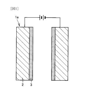
Fig. 1 is a schematic diagram schematically showing a configuration of a
diamond electrode in a first embodiment of the present invention.
Fig. 2 is a flowchart of a method for manufacturing the electrode in the first
embodiment of the present invention.
Fig. 3 is a schematic diagram schematically showing a configuration of a
diamond electrode in a second embodiment of the present invention.
Fig. 4 is a flowchart of a method for manufacturing the electrode in the
second
embodiment of the present invention.
Fig. S is a schematic diagram schematically showing a state in which 0. 1
mot/litters of an aqueous sodium sulfate solution is supplied to an
electrolytic treatment
-5-
CA 02703093 2010-04-20
device where the diamond electrodes are used for both of an anode and a
cathode.
DESCRIPTION OF THE REFERENCE SIGNS
la, lb electrode, 2 substrate, 3 diamond film, 4 0.1 mot/l of aqueous sodium
sulfate solution, 5 electrolytic treatment device
BEST MODES FOR CARRYING OUT THE INVENTION
Embodiments of the present invention will be described hereinafter with
reference to the drawings. The same or corresponding portions are represented
by the
same reference characters, and description thereof will not be repeated.
(First Embodiment)
Fig. I is a schematic diagram schematically showing a configuration of a
diamond electrode in a first embodiment of the present invention. As shown in
Fig. 1,
an electrode 1 a in the present embodiment includes a substrate 2 and a
conductive
diamond film 3 covering one surface of substrate 2. It is noted that a
monocrystalline
silicon wafer, for example, can be used as substrate 2. Polycrystalline
silicon may be
used as substrate 2.
Fig. 2 is a flowchart of a method for manufacturing the electrode in the first
embodiment of the present invention. Next, the method for manufacturing
electrode I a
in the present embodiment will be described with reference to Fig. 2.
As shown in Fig. 2, a step of seeding a substrate (S 10) is performed.
Specifically, a surface of the substrate is seeded with diamond powder of
#5000.
Thereafter, a step of cleaning and drying the substrate (S20) is performed.
After
drying, a step of forming a conductive diamond film (S30) is performed. As
long as
the diamond film can be formed, a method for forming the film is not
particularly limited.
In step (S 10), the step of seeding the substrate is for colliding fine
abrasive
grains with the surface of the silicon substrate and making many scratches
prior to
cleaning, so as to promote film formation by the CVD treatment by using the
scratches
as nuclei.
Next, in step (S20), cleaning is performed by ultrasonic cleaning for I to 5
-6-
CA 02703093 2010-04-20
minutes with an organic solvent such as alcohol and acetone. It is noted that
the
frequency at the time of the ultrasonic cleaning varies depending on the size
of a
cleaning vessel.
Next, step of forming a conductive diamond film (S30) is performed.
Specifically, the conductive diamond film is formed by the hot filament CVD
method on
one surface or a plurality of surfaces of cleaned substrate 2. Conditions such
as the
synthesis pressure of 60 Torr, the hydrogen flow rate of 3000 sccm and the
methane
flow rate of 90 sccm can be used as synthesis conditions. Furthermore,
diborane gas is
used as a boron source and a flow rate of the diborane gas is set such that
the
concentration thereof is 0.3% with respect to the methane. The temperature of
the
substrate is set to 9000 . It is noted that the thickness of the diamond film
is
controlled by changing the synthesis time. The method for forming the diamond
film in
above step (S30) is not necessarily limited to the above method, but other
generally-
known methods can be employed.
It is noted that a method such as the hot filament method, the microwave
plasma
CVD method and the ECR jet method can be used as the CVD method for
synthesizing
the diamond film in above step (S30). In particular, in order to form a good-
quality
diamond film for the electrode, it is preferable to use the hot filament
method and the
microwave plasma CVD method. The reason why the hot filament CVD method is
preferable is that it is suitable for synthesis in a large area. Although not
suitable for
film formation in a large area, it is desirable to use the microwave plasma
CVD method
in order to synthesize a high-quality diamond film having a low impurity
concentration,
for example. Thus, also in the present invention, it is preferable to use the
hot filament
CVD method as a method for film formation.
The gas used in the CVD method includes hydrogen gas and carbon-containing
gas such as methane and acetone as described above. As a doping element for
providing conductivity to the diamond film, boron is the most effective, but
phosphorus
may be used in some cases. As an ingredient of boron, a boron-containing
substance
-7-
CA 02703093 2010-04-20
such as aforementioned diborane gas and boric acid is used. Thus, also in the
present
embodiment, the diborane gas is used to supply boron, so as to provide
conductivity to
the diamond film.
In order to study the conditions for formation of the diamond film, the
inventors
conducted an experiment on formation of the diamond film by using methane gas
as
ingredient gas, when the concentration of the methane gas with respect to the
hydrogen
gas is varied. A result thereof is shown in Table 1.
[Table 1]
Methane Thickness of Oxygen
Concentration Diamond Film Synthesis Rate Generation
Potential
0.2% 2.4 m 0.06 m/hr 2.3V
1% 14.84m 0.37Etm/hr 2.2V
2% 31.2 m 0.78 m/hr 2.OV
3% 50.5 m 1.26 m/hr 1.8V
4% 61.2 m 1.53 m/hr 1.5V
Table I shows "thickness" and "oxygen generation potential" of the synthesized
diamond film when the diamond film is formed by the hot filament CVD method by
using methane and a diamond is synthesized onto the silicon substrate for 40
hours in
respective methane concentrations.
According to the result in Table 1, when the methane concentration is less
than
or equal to 0.2%, a synthesis rate of the diamond film is extremely low. It
takes too
long to form the film having a film thickness of greater than or equal to 10
m, which is
not practical. Furthermore, it is seen that, when the methane concentration
exceeds
3%, the quality of the diamond is degraded, and therefore, the oxygen
generation
potential is low, that is, the performance as the electrode for use in
electrolysis is not
sufficient.
Therefore, for example, in a case where methane is used as the carbon-
-8-
CA 02703093 2010-04-20
containing gas, it is preferable that the proportion of the carbon-containing
gas (methane
gas) to the hydrogen gas ranges between 1% and 3%.
(Second Embodiment)
Fig. 3 is a schematic view schematically showing a configuration of a diamond
electrode in a second embodiment of the present invention. As shown in Fig. 3,
an
electrode lb in the present embodiment differs from that in the first
embodiment only in
that electrode lb includes conductive diamond films 3 covering two surfaces,
that is, the
main surface of substrate 2 and the back surface thereof
In a case where an electrolysis device of a hybrid structure having more than
one
set of the electrodes is formed, the electrode includes diamond films 3 on
both surfaces,
that is, the main surface of substrate 2 and the back surface thereof The
conditions
such as the film thickness and the film quality of the components forming
electrode 1 b
are the same as those in the first embodiment. Furthermore, the film thickness
and the
film quality of diamond film 3 formed on the back surface of substrate 2 are
similar to
those of diamond film 3 formed on the front surface of substrate 2.
Fig. 4 is a flowchart of a method for manufacturing the electrode in the
second
embodiment of the present invention. Step of seeding the substrate (S 10) to
step of
forming the diamond film on the main surface of the substrate (S30) are the
same as
those in the method for manufacturing the electrode in the first embodiment
shown in
Fig. 2. The method in the second embodiment differs from that in the first
embodiment
only in that a step of forming the diamond film on the back surface of the
substrate in a
similar manner (S40) is added after step (S30).
Example 1
Although the present invention will be hereinafter described more specifically
according to examples, the present invention is not limited to these examples.
In the present example, a monocrystalline silicon wafer having an orientation
of
(100) and a diameter of 6 inches is prepared for use as the substrate, when
the thickness
of the wafer is varied differently as shown in Table 2. As in the specific
example of the
-9-
CA 02703093 2010-04-20
manufacturing method described above, each surface of monocrystalline silicon
is
seeded with the diamond powder of #5000, and then, the wafer is cleaned and
dried.
On one main surface of the substrate prepared in such a manner, a conductive
diamond
film is formed by the hot filament CVD method. The thickness of the diamond
film is
controlled by changing the synthesis time.
(Comparative Example)
As comparative examples, a diamond film having a thickness of less than 10 tm
(comparative example 1), a diamond film having a thickness exceeding 70 m
(comparative example 2) and diamond films having a ratio between the thickness
of the
diamond film and the thickness of the substrate is outside the scope of claims
(comparative examples 3 to 6) are fabricated under the same conditions as
those in the
above, and comparative evaluation is conducted.
(Method for Measuring)
An electrolytic treatment experiment is conducted by using the diamond
electrodes fabricated by the above-described method, and an experiment is
conducted to
check durability of the respective electrodes. As shown in Fig. 5, 0.1
mol/litters of a
circulating aqueous sodium sulfate solution 4 is supplied to an electrolytic
treatment
device 5 where the diamond electrodes are used for both of an anode and a
cathode, and
the electrolytic treatment is performed. A spacing between the electrodes is
maintained
at 10 mm and the current density is maintained at 0.3 A/cm2. The durability is
checked
by stopping the electrolytic experiment every 100 hours to observe the
condition of the
diamond film, and extending the test time for another 100 hours if an
abnormality is not
found. Based on such a test, a time period during which the experiment can be
continued until the diamond film is peeled off is recorded. A result thereof
is shown in
Table 2.
-10-
CA 02703093 2010-04-20
[Table 2]
Thickness of Thickness of Thickness of Film ( m)/
No. Substrate Diamond Thickness of Substrate Durability
(mm) Film ( m) (mm /1000
1 3 10 0.003 3 peeling of film after
4800 hours
2 15 15 0.001 peeling of film after
1600 hours
3 1 20 0.020 peeling of film after
3400 hours
4 12 20 0.0017 peeling of film after
3100 hours
30 35 0,0012 peeling of film after
1700 hours
6 23 40 0.0017 peeling of film after
3500 hours
7 3 52 0.017 peeling of film after
5700 hours
8 30 60 0.002 peeling of film after
4900 hours
9 3 65 0.022 peeling of film after
1800 hours
Comparative 3 8 0.0027 peeling of film after
Example 1 500 hours
Comparative 6 75 0.0125 peeling of film after
Example 2 600 hours
Comparative 15 12 0.00080 peeling of film after
Example 3 500 hours
Comparative 1 25 0.025 peeling of film after
Example 4 600 hours
Comparative 50 40 0.00080 peeling of film after
Example 5 700 hours
Comparative 2 52 0.026 peeling of film after
Example 6 700 hours
(Result of Measuring)
As shown in Table 2, the diamond film of the electrode fabricated under the
5 conditions satisfying the numerical formulas described in the above scope of
claims as to
the thicknesses of the substrate and the diamond film that are used as the
electrode
-11-
CA 02703093 2010-04-20
endures for about 1500 to 5000 hours and has a long life. On the other hand,
it is seen
that the diamond film of the electrode fabricated under the conditions that
are outside
the above scope of claims, which is indicated by comparative examples 1 to 6,
is peeled
off only after 500 to 700 hours and has a shortened life.
As described above, according to the present example, it can be found out
that,
assuming that the thickness of the silicon substrate is T ( m) and the
thickness of the
conductive diamond film formed on one main surface of the silicon substrate is
t ( m),
the electrode formed such that the ratio between the thickness of the silicon
substrate
and the thickness of the conductive diamond film is 0.0010 5 t/T 5 0.022 and
10 < t S
70 can be operated for a long time without peeling of the diamond film and
practical
application can be expected. Furthermore, as a result of detailed observation
of the
result of the example, it is found that the diamond electrode can endure
further
prolonged use without peeling when the ratio indicated by the above numerical
formulas
is preferably 0.0015 <_ t/T <_ 0.020, and more preferably 0.0020 <_ t/T <_
0.018.
Conversely, it can be said that the diamond film of the electrode formed under
the conditions that are outside the conditions of the above numerical formulas
is peeled
off in a short time and the stable quality cannot be ensured.
It should be understood that the embodiments disclosed herein are illustrative
and not limitative in any respect. The scope of the present invention is
defined by the
terms of the claims, rather than the description above, and is intended to
include any
modifications within the scope and meaning equivalent to the terms of the
claims.
INDUSTRIAL APPLICABILITY
The diamond electrode in the present invention is particularly suitable for
the art
related to an electrode used for waste water treatment or production of
functional water
by using electrolysis.
-12-