Note: Descriptions are shown in the official language in which they were submitted.
CA 02703205 2010-04-21
WO 2009/058183
PCT/US2008/011303
RFID ANTENNA SYSTEM AND METHOD
FIELD OF THE INVENTION
The present invention relates to the field of radio frequency identification
("RFID") communications, and in particular towards RFID transponder
configurations.
BACKGROUND OF THE INVENTION
Radio frequency identification (RFID) devices are becoming increasingly
popular for a variety of industrial, retail, transportation, and other
applications. RFID
technology provides a positive identity for any object, person, or the like,
bearing an
RFID transponder through the use of a passive, radio frequency signal. In a
typical
application, an RFID transponder comprises an antenna and an integrated
circuit.
When a separate RFID reading device broadcasts a radio frequency signal, the
signal
interacts with the RFID transponder antenna. The transponder antenna converts
put of
the received RF signal energy into an electrical current. This electrical
current powers
the integrated circuit. The integrated circuit then modulates its impedance to
create a
return RF signal. This return RF signal is then detected by the antenna in the
RFID
reading device. This modulated, RF return signal carries encoded data about
the
transponder based on the data previously stored in the integrated circuit. For
example,
the serial number of the transponder may be returned to the RFID reading
device via
this modulated RF signal. Finally, the RFID reading device decodes the signal
returned
from the transponder to complete the identification.
RFID transponders are being integrated into a growing number of applications.
Employee identity badges, animal identity devices, retail pricing and
inventory devices,
retail security devices, manufacturing product and material tracking devices,
vehicle
1
CA 02703205 2010-04-21
WO 2009/058183
PCT/US2008/011303
identification devices, and the like, are just a few examples of the expanding
area of
applications for RFID technology. RFID transponders are ideally suited for
integration
with a wide variety of products and in a wide variety of situations. RFID
transponders
may be purely passive devices where all of the energy for operating the
integrated
circuit is derived from the broadcast RF signal. Alternatively, active RFID
systems may
incorporate an on-board battery to provide power to the identity chip and/or
power for
the transponder's return RF signal. In fixed systems, such as motor vehicle
transponders used for automated toll collection, the additional cost of the on-
board
battery is easily justified by the improved performance of the device.
Conversely, in
cost sensitive applications such as retail pricing and security tags, the RFID
transponder
device must be as inexpensive as possible and is therefore, typically, a
passive device.
The on-board antenna is a key enabling technology for RFID transponder
devices. The broadcast RF energy may be in the form of a magnetic field, an
electric
field, or a mixed field as in typical radio signal broadcast. The transponder
antenna is
designed with a shape and a size based on the characteristics of the broadcast
RF
energy such as the field type and the signal frequency. Moreover, the design
of RFID
tags typically requires matching the antenna impedance and load impedance,
usually by
a matching circuit, for maximizing the RF power from the reader's
interrogation or
command signal received at the tag antenna to be delivered to the RFIC with
minimum
loss, and thereby achieve optimum tag sensitivity. Theoretically, maximum
power
delivery is achieved by conjugate impedance matching, which demands that the
impedance from the antenna be, as closely as possible, the mathematical
conjugate of
the RFID input impedance. This represents an ideal impedance match.
2
CA 02703205 2010-04-21
WO 2009/058183
PCT/US2008/011303
In many applications, it is desirable to reduce the overall size or
"footprint" of a
particular RFID device. The reduced size may be required for inclusion on or
in retail
goods having small dimensions. Alternatively, it may simply be desirable to
make the
RFID device as inconspicuous as possible. While technology exists to
drastically
reduce the size of an IC component of an RFID device, similar miniaturization
of the
antenna of an RFID device can result in a significant reduction in
performance. As
stated above, a particular IC and antenna of an RFID device ideally have
matched
impedance characteristics. By reducing the overall size of the RFID device,
and thus
the antenna, it may prove difficult to adequately provide the impedance
characteristics
for efficient function of the device. As such, the RFID may suffer from
inefficient
power transfer to the IC, a reduced operating range with respect to an
interrogator, and
a weak return signal in response.
In addition, an antenna connected to a RFID tag is generally designed for
operation on a specific or narrow range of substrates to which it may be
attached.
Other substrates may cause the radiation efficiency of the antenna to
deteriorate from
the designed optimal mounting substrates. Thus, the antenna, and consequently
the
RFID device, will no longer function as intended. This loss of antenna
efficiency may
be due to a number of variable packaging factors. For example, each substrate
has its
own dielectric and conductive characteristics that typically affect the
impedance
matching between the wireless communication device and its antenna. Impedance
matching ensures the most efficient energy transfer between an antenna and the
wireless communication device, as discussed above, and placement of an RFID
device
in proximity to a surface having dielectric and conductive properties outside
of a
particular range may reduce the performance of the RFID device. These adverse
3
CA 02703205 2010-04-21
WO 2009/058183
PCT/US2008/011303
effects to the performance of an RFID device may also be experienced upon the
inclusion or integration of an electronic article surveillance ("EAS") tag or
device.
Such EAS devices often include a magneto-acoustic mechanism having one or more
metallic components that may subsequently interfere with or reduce the
performance
characteristics of a particular RFID device.
In view of the above, it would be desirable to provide an RFID device having a
reduced footprint while providing for efficient operation on a variety of
surfaces and/or
in combination with an EAS tag.
SUMMARY OF THE INVENTION
The present invention advantageously provides a method and system for an
RFID/EAS device. In accordance with a first aspect of the present invention,
an RFID
device is provided having a dielectric substrate body, an antenna disposed on
the
substrate body, and a first spacing element, where at least a portion of the
substrate is
wrapped around a portion of the spacing element.
The substrate may be constructed from a material including at least one of
polyimide, polyester, fiberglass, ceramic, plastic, and paper, and the antenna
may be
constructed from a material including at least one of copper, aluminum and
conductive
ink. The antenna may include an electrically conductive material patterned on
a surface
of the substrate body. In particular, the pattern includes a plurality of
polygons, such as
one or more polygons having a substantially rectangular shape with squared or
rounded
corners. The pattern can also include meanderline (meandering pattern)
segments. The
plurality of polygons of the antenna may be non-continuous and/or include a
non-
conductive opening or break therein to thereby provide a single electrically
conductive
4
CA 02703205 2015-03-11
77496-335
path. Further, one or more capacitors may be disposed on the substrate and in
electrical
communication with the antenna.
In another aspect of the present invention, an RFID/EAS device is provided.
The RFID/EAS device may generally include a dielectric substrate body, an
antenna disposed
on the substrate body, a first spacing element, and a second spacing element.
In addition, an
EAS element may be disposed between the first and second spacing elements, and
at least a
portion of the substrate body may be positioned to surround a portion of both
the first and
second spacing elements. The EAS element may include an acousto-magnetic
device and/or a
microwave device.
In yet another aspect of the present invention, a method of assembling an
RFID/EAS device is provided, where the method includes the steps of providing
an RFID
device having a dielectric substrate body and an antenna disposed on the
substrate body. The
method further includes positioning an EAS element between a first spacing
element and a
second spacing element, and subsequently wrapping at least a portion of the
RFID device
around at least a portion of the first and second spacing elements.
According to one aspect of the present invention, there is provided a radio
frequency identification (RFID)/electronic article surveillance (EAS) device,
the device
comprising: a dielectric substrate body; an antenna disposed on the substrate
body; a first
spacing element formed separately from the substrate body, the first spacing
element having
an EAS element embedded within the first spacing element; and at least a
portion of the
antenna on the substrate body being wrapped around at least a portion of the
first spacing
element having the embedded EAS element.
According to another aspect of the present invention, there is provided a
combination radio frequency identification (RFID)/electronic article
surveillance (EAS)
device, the device comprising: an EAS element; a dielectric substrate body; an
antenna
disposed on the substrate body; a first spacing element formed separately from
the substrate
body, at least a portion of the first spacing element being in contact with at
least a portion of
the EAS element; a second spacing element formed separately from the substrate
body, the
5
CA 02703205 2015-03-11
77496-335
second spacing element being separate from the first spacing element, at least
a portion of the
second spacing element being in contact with at least a portion of the EAS
element; and at
least a portion of the antenna on the substrate body being wrapped around the
EAS element
and the at least the portion of the first and second spacing elements.
According to still another aspect of the present invention, there is provided
a
method of assembling a radio frequency identification device (RFID)/electronic
article
surveillance (EAS) device, comprising the steps of: providing an RFID device
including a
dielectric substrate body and an antenna disposed on the substrate body;
positioning an EAS
element between a first spacing element and a second spacing element, the
second spacing
element being separate from the first spacing element, the first spacing
element and second
spacing element being formed separately from the substrate body; and wrapping
at least a
portion of the RFID device around at least a portion of the first and second
spacing elements.
5a
CA 02703205 2010-04-21
WO 2009/058183
PCT/US2008/011303
BRIEF DESCRIPTION OF THE DRAWINGS
A more complete understanding of the present invention, and the attendant
advantages and features thereof, will be more readily understood by reference
to the
following detailed description when considered in conjunction with the
accompanying
drawings wherein:
FIG. 1 illustrates of an embodiment of an RFID device constructed in
accordance with the present invention;
FIG. 2 illustrates an alternate embodiment of an antenna pattern for an RFID
device constructed in accordance with the present invention;
FIG. 3 illustrates yet another embodiment of an antenna pattern for an RFID
device in constructed accordance with the present invention;
FIG. 4 illustrates the use of one or more capacitors electrically coupled to
the
antenna in constructed accordance with the present invention
FIG. 5 illustrates the ability of the antenna to be wrapped around a spacer
element in accordance with the present invention; and
FIG. 6 illustrates an alternate configuration of the spacer element used in
accordance with the present invention.
6
CA 02703205 2010-04-21
WO 2009/058183
PCT/US2008/011303
DETAILED DESCRIPTION OF THE INVENTION
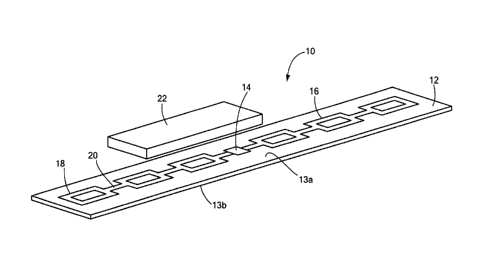
Referring now to the drawing figures in which like reference designators refer
to like elements, there is shown in FIG. 1 a diagram of an exemplary apparatus
constructed in accordance with the principles of the present invention and
designated
generally as "10". Apparatus 10 is an RFID device that may generally include a
substrate body 12, with an integrated circuit ("IC") component 14 coupled to
the
substrate body 12, as well as an antenna 16 disposed on the substrate body 12
in
electrical communication with the IC component 14. Antenna 16 may generally
include a pattern of conductive material. In particular, the antenna 16 may
include a
plurality of substantially square or rectangular shaped polygons 18 having
squared or
rounder corners, where a portion of the polygons 18 are hollowed out, i.e., do
not
contain a conductive material. The plurality of polygons 18 may be
electrically
coupled to one another by a strip or portion of conductive material 20
connecting each
polygon 18, and further connecting the plurality of polygons 18 to an IC
component 14.
Although not shown, it is also contemplated that pattern of antenna 16 can
take the
form of a meanderline segment such that the overall length of antenna 16 is
greater than
the distance from the end point of the antenna coupled to IC component 14 to
the outer
edge of substrate body 12. This can be accomplished, for example, by allowing
antenna 16 to "meander" back and forth along substrate body 12 as antenna 16
runs
from IC component 14 to the outer edge of substrate body 12. Meanderline
segments
can be used separately or in connection with one or more polygons. The antenna
16
may further include a conductive coupling (not shown) between first and second
portions of the antenna 16 on either side of IC component 14. The coupling can
7
CA 02703205 2010-04-21
WO 2009/058183
PCT/US2008/011303
provide a current loop to increase or otherwise optimize the performance
characteristics
of the antenna 16.
Apparatus 10 may further include a spacing element 22, where at least a
portion
of the substrate body 12 surrounds at least a portion of the spacing element
22.
Discussed below in detail, the RFID device 10 may also include an EAS element
such
as an acousto-magentic device (not shown in FIG. 1), coupled to at least one
of the
substrate body 12 and/or spacing element 22.
In particular, the substrate body 12 may generally define a first surface 13a
and
a second surface 13b opposite the first surface 13a, where the first surface
13a may
receive the IC component 14 and at least a portion of the antenna 16. The
first surface
13a may include dielectric properties as to reduce or eliminate the likelihood
of
interference with the antenna 16 or to otherwise prevent shorting the antenna
16 and/or
the IC component 14. The second surface 13b may be suited for fixation or
other
coupling to a particular item, packaging, or the like. For example, the second
surface
13b may include an adhesive property or the like to facilitate placement of
the RFID
device 10. In addition, the second surface 13b may have similar dielectric
properties to
that of the first surface. The substrate body 12 may include one or more
layers of a
substrate constructed from a flexible material, such as an organic material
like
polyimide or polyester for example. The substrate body 12 may have an
elongated,
rectangular shape appropriately sized for a given application, although a
myriad of
shapes and sizes may be used for varied circumstances.
The IC component 14 of the RFID device 10 may be coupled to or otherwise
positioned on the first surface 13a of the substrate body 12. The IC component
14 may
generally include an integrated circuit device capable of storing multiple
bits of data,
8
CA 02703205 2010-04-21
WO 2009/058183
PCT/US2008/011303
and may further be capable of modulating current in the antenna of the RFID
device 10
to thereby encode data onto an RF signal. In particular, the IC component 14
may
include a semiconductor-based device, such as a silicon chip, and may further
include
active and/or passive elements such as transistors, resistors, capacitors, and
the like,
integrated thereon. For example, the IC component 14 may include a passive
network
of resistors, capacitors, and/or inductors that exhibits a resonance response
to an
incoming RF signal. In addition, the IC component 14 may include a diode
device to
simply rectify the incoming RF signal. The IC component 14 may further include
a
fixed response frequency and/or identifying data pattern, and alternatively
may include
a response frequency and/or identifying data pattern that is programmable
and/or re-
programmable.
The RFID device 10 of the present invention further includes antenna 16
disposed on the first surface 13a of the substrate body 12, where the antenna
16 is able
to conduct an RF signal. The antenna 16 may include a patterned configuration
of
conductive material in electrical communication with the IC component 14 to
transmit
a signal both to and from the IC component 14. The pattern of the antenna 16
may be
modified and/or selected to provide desired impedance characteristics to
compliment
the electrical characteristics of the IC component 14 for optimal use and
performance
of the RFID device 10. The antenna 16 may be comprised of a material having
sufficiently high electrical conductivity, such as a metallic material
comprising copper
(Cu) or aluminum (A1), or a microwave conductive carbon fiber. The antenna 16
may
be patterned onto the first surface 13a of the substrate body 12 utilizing any
commonly
known patterning method such as but not limited to a photolithographic, ion
etching,
chemical etching, or vapor deposition process. The antenna 16 may generally
include a
9
CA 02703205 2010-04-21
WO 2009/058183
PCT/US2008/011303
dipole configuration with the IC component, 14 although a monopole
configuration
may be equally applicable with the present invention.
In addition, the antenna 16 may be patterned to provide either a single
conductive path or, alternatively, multiple electrical paths in series. For
example, the
antenna pattern may include a plurality of connected polygons 18 providing a
path for
conducting a desired signal. Each polygon 18 may have a substantially
continuous
shape, where a plurality of the polygons 18 are connected to one another to
define a
series of conductive paths therethrough. The polygons of a particular antenna
pattern
may be "hollowed" or have varying dimensions or thickness of conductive
material in
order to provide a desired impedance for a particular application.
Alternatively, as shown in FIG. 2, antenna 16 may include a patterned of "open-
ended" polygons 18 that provide a single electrically conductive flow path.
The pattern
of polygons 18 in FIG. 2 are non-continuous, i.e., a side or portion of each
polygon 18
is non-conductive, thereby providing a single electrically conductive flow
path through
the length of the antenna 12. In FIG. 2, the polygons 18 are configured in an
alternating pattern. Similar to the previous antenna arrangement depicted in
FIG. 1, the
plurality of non-continuous polygons 18 may be in electrical communication
with one
another by a link or deposit of conductive material coupling the plurality of
polygons
18 together, as well as coupling the antenna pattern to the IC component 14.
In
addition, should the antenna 16 include a dipole configuration extending on
either side
of the IC component 14, there may be a conductive strip or portion 23
connecting the
two sides of the antenna to one another to form a current loop or electrical
path external
to or independent of the IC component 14, as shown in FIG. 2.
CA 02703205 2010-04-21
WO 2009/058183
PCT/US2008/011303
FIG. 3 illustrates another antenna configuration whereby each polygon 18 is
non-contiguous, as in the embodiment shown in FIG. 2. However, in this
configuration, the orientation of each polygon 18 is repeated. The present
invention is
not limited to any particular orientation of polygons 18 and may include a
combination
of patterns and not only those depicted in FIGS. 2 and 3. By varying the
patterns of the
polygons 18 (or meanderline), a different overall impedance can be obtained.
Of note, although the embodiments shown in FIGS. 2 and 3 show symmetric
antenna segments on each side of IC chip 14, the present invention is not
limited to
such. It is contemplated that asymmetric antenna segments can be implemented,
for
example, by employing different numbers of polygons 18 on each side of IC chip
14.
Similarly, as shown in the exemplary embodiments of FIGS. 1-3, the capacitive
and inductive portions of the impedance used to match the antenna to IC chip
14 can be
derived from antenna 16 itself without the need for external discrete devices.
By
varying the length of the electrically conductive path of antenna 16, the
capacitive and
inductive portions of the impedance can be altered. By way of non-limiting
example,
extending the length of antenna 16 results in an increase in the capacitive
and inductive
portions of the impedance. In a case such as that shown in FIG. 1, where the
resultant
length of antenna 16 exceeds the length of the spacer 22 (or EAS element), as
discussed
below in detail, substrate body 12 (along with antenna 16) can be wrapped
around the
spacer to minimize overall package size.
In FIG. 4, one or more discrete capacitors 26 may be electrically coupled to
either or both ends of the antenna 16 to provide the desired electrical
capacitive
characteristics of the RFID device. As used herein, the term "capacitor" is
intended to
include any element or structure exhibiting capacitance properties. For
example, it may
11
CA 02703205 2010-04-21
WO 2009/058183
PCT/US2008/011303
include an extended portion of the antenna 16 or the like, and is not limited
to a
configuration of a discrete "capacitor" component made of two charged
conducting
surfaces having opposite polarities separated by a dielectric. Although not
necessary
based on the use of electrically conductive path length of antenna 16 itself
to create a
matching impedance, discrete capacitors 26 and/or discrete inductors (not
shown) can
be implemented in any of the antenna arrangements described herein.
As described above, the RFID device 10 of the present invention may further
include one or more spacing elements 22 coupled to the substrate body 12 to
offset or
otherwise manipulate the position of the substrate body 12, or any portions
thereof
relative to one another. Each spacing element 22 may define a substantially
planar
body having non-conductive and/or dielectric properties, and may be
constructed from
a nonconductive plastic, polymer, or other suitable insulating material. For
example,
the spacing element 22 may constitute a substantially rectangular-shaped
portion of
insulating foam, where the spacing element has a thickness of less than
approximately 3
mm.
FIG. 5 shows an exemplary configuration of the RFID device 10 of the present
invention using any of the aforementioned antenna configurations. As discussed
above,
IC component 14 is coupled to a non-conductive surface of the substrate body
12. The
antenna 16 extends from and is in electrical with the IC component 14 on the
substrate
body 12 to provide the desired impedance characteristics as described above.
At least a
portion of the substrate body 12 of the RFID device 10 may then be positioned
about an
exterior perimeter or portion of the spacing element 22. Subsequently, the
substrate
body 12 may be substantially wrapped, folded or otherwise disposed around the
spacing element 22 such that both the IC component 14 and the antenna 16 are
facing
12
CA 02703205 2010-04-21
WO 2009/058183
PCT/US2008/011303
or otherwise in proximity to the spacing element 22. Of note, although FIG. 5
shows a
spacing element 22 that is separate from substrate body 12, it is contemplated
that a
cover stock (not shown) can be positioned over substrate body 12 such that
when
substrate body 12 is wrapped over itself, the cover stock serves as spacing
element 22.
The thickness of the cover stock, e.g., cardboard, paper, plastic, etc., can
be varied to
establish a desired resultant spacing when substrate body 12 is wrapped over
itself.
As the substrate 12 is essentially wrapped around and over spacing element 22,
the resulting RFID device 10 has virtually the same physical dimensions as the
spacer
element without compromising or reducing the actual length of the antenna 16.
The
spacing element 22 prevents the antenna 16 from shorting out since it provides
a buffer
between opposing portions of the antenna 16. The result is that the overall
impedance
of the antenna 16 when wrapped over spacing element 22 matches the impedance
of IC
component 14 but the size of the RFID device 10 is significantly reduced due
to the
ability of the substrate 12 to fold over the spacing element 22. Thus, due to
the
"wrapping" of the substrate 12 over the spacing element 22, RFID device 10
achieves
impedance matching between the IC component 14 and the appropriate antenna
pattern
yet drastically reduces its overall size, while at the same time preventing a
short in the
antenna or circuitry on the device 10 due to the spacing element 22.
The device of the present invention may further include an electronic article
surveillance ("EAS") element 24 coupled to the substrate body 12. The EAS
element
24 may include an acousto-magnetic device having a strip of amorphous ferro-
magnetic
metal, where the strips are free to oscillate mechanically and are identified
by their
resonating response to an induced magnetic field.
13
CA 02703205 2010-04-21
WO 2009/058183
PCT/US2008/011303
Alternatively, the EAS element may include a microwave device having a non-
linear element (such as a diode) coupled to a microwave and electrostatic
antenna. One
antenna emits a low-frequency (about 100 kHz) field, and another one emits a
microwave field, where the device acts as a mixer reemitting a combination of
signals
from both fields to trigger an alarm. Additional suitable EAS devices and/or
tags as
known in the art may be equally suitable for use with present invention.
Now referring to FIG. 6, the EAS element 24 may be embedded or otherwise
placed between one or more spacing elements 22, while the substrate body 12
remains
disposed about an outer perimeter of the one or more spacing elements 22. In
particular, the EAS element 24 may be disposed between a first spacing element
22a
and second spacing element 22b (collectively referred to herein as "spacing
elements
22"), where the substrate body 12 having the IC component 14 and antenna 16 is
disposed about a portion of the perimeters of the first and second spacing
elements 22,
resulting in the folded configuration illustrated in FIG. 5. As the substrate
body 12 and
the EAS element 24 are not in electrical with one another, the desired
impedance
characteristics of the antenna/IC component pairing remains intact while
allowing the
RFID device 10 to provide both an identification as well as article
surveillance
function.
In an exemplary use of the RFID device 10, the RFID device 10 may be coupled
to or otherwise positioned onto an article or item. The RFID device 10 may
include the
EAS element 24 embedded within one or more spacing elements. Moreover, due to
the
wrapping of at least a portion of the device about one or more spacing
elements, the
overall footprint of the RFID device is substantially reduced.
14
CA 02703205 2015-03-11
77496-335
It will be appreciated by persons skilled in the art that the present
invention is
not limited to what has been particularly shown and described herein above. In
addition, unless mention was made above to the contrary, it should be noted
that all of
the accompanying drawings are not to scale. A variety of modifications and
variations
are possible in light of the above teachings without departing from the scope
of the invention, which is limited only by the following claims.
=