Note: Descriptions are shown in the official language in which they were submitted.
CA 02703342 2013-11-15
1
SECURITY ELEMENT HAVING REFLECTIVE AND LIGHT
SCATTERING LAYERS
The invention relates to improvements in security
elements for use in or on security substrates. In
particular the invention is concerned with security
elements having public recognition features.
. .
It is widely known to. use in banknotes, passports,
certificates and other security documents security
elements, such as security threads-on strips. These
security elements are partially or wholly embedded in a
paper or plastic substrate, and generally provide different
viewing conditions depending on whether the security
document is viewed in transmitted or reflected light.
EP-A-319157, for example, describes a security element
made from a transparent plastic film provided with a
continuous reflective metal layer, such as aluminum, which
has been vacuumed deposited on the film. .The metal layer is
partially demetallised to provide clear demetallised
regions that form indicia. When wholly embedded within a
paper substrate the security element is barely visible in
reflected light. However, when viewed in transmitted light
the indicia can be clearly seen highlighted against the
dark background of the metallised area of the security
element and adjacent areas of the paper. Such elements can
also be used in a security document provided with repeating
windows in at least one surface of the paper substrate in
which the security element is exposed. A security document
CA 02703342 2010-04-22
WO 2009/053673
PCT/GB2008/003505
2
of this type, when viewed in transmitted light, will be
seen as a dark line with the indicia highlighted. When
viewed in reflected light on the windowed side, the bright
shiny aluminum portions are readily visible in the windows.
This security element has been highly successful within the
market place and is supplied under the trade mark
CleartextO.
For a number of years banknote issuing authorities
have had an interest in combining both the public
recognition properties of CleartextO with the covert
properties of a machine-readable feature. To this end it is
preferable to utilise machine-readable features that can be
read using detectors already available to the banknote
issuing authorities. Examples of such machine-readable
devices are described in WO-A-92/11142 and EP-A- 773872.
The security device of WO-A-92/11142 is an attempt to
provide this combination. A security device conforming to
this specification has been used commercially with some
success. A central region of the security device has a
metallic appearance with clear regions forming characters;
on either side of this central strip in the width
direction, there are layers of magnetic material with
obscuring coatings to provide the necessary magnetic
component. This is, however, a generally unsatisfactory
means of achieving the combination of the appearance of
Cleartexte with the required magnetic properties. The
magnetic properties are satisfactory, but the requirement
to place the magnetic layers on either side of a central
region means that the latter must be relatively narrow with
CA 02703342 2012-06-19
3
high, and therefore not easily legible. Additionally, the
structures of the devices described in WO-A-92/11142 are
very complex and present substantial lateral registration
problems in depositing the various layers; a mis-
registration of even 0.25mm or so can allow the presence of
the dark magnetic oxide to be apparent to the naked eye,
thus revealing its presence and seriously detracting from
the aesthetic appearance of the security element.
A more satisfactory solution, from the processibility,
ease of character recognition and aesthetics points of
view, would be to manufacture a device of the kind
described in EP-A-0319157 from a metal which is itself
magnetic. Thus the size of the characters, and ratio of
character height:width of the Cleartext product can be
maximised to the benefit of visibility of the Cleartext0
feature, whilst providing direct compatibility with
existing magnetic detectors.
One means of achieving this is disclosed in Research
Disclosure No. 32354 of March 1991 (Knight, M.R.M.,
"Security device for banknote paper", Research Disclosure
Journal, Database Number 323054, March, 1991). In this
Research Disclosure, a magnetic material-is deposited onto
a flexible substrate by vacuum sputtering or other known
techniques; the non-metallised regions are created by
selective printing of a resist layer and subsequent
chemical etching. The disclosed magnetic materials may be
nickel, cobalt, iron or alloys thereof with a preferred
combination of cobalt:nickel in the ratio 85:15%. The
disadvantage of this method is that vacuum deposition of
cobalt:nickel to the necessary thickness is a relatively
slow process and somewhat wasteful of cobalt, an expensive
ak 02703342 2010-04-22
WO 2009/053673
PCT/GB2008/003505
4
cobalt:nickel to the necessary thickness is a relatively
slow process and somewhat wasteful of cobalt, an expensive
material. Furthermore, subsequent to this vacuum deposition
process, further significant processing is required to etch
the characters. The resultant product is therefore
relatively expensive.
A further alternative approach is described in
EP A-773872 wherein a magnetic metal is deposited on a film
of polymeric substrate as the substrate passes through a
solution containing the magnetic metal. A preparatory
priming seed print operation ensures that magnetic metal is
deposited on the substrate in a chosen pattern such that
when the security product is produced, the magnetic metal
on the security element has a specific pattern and provides
both a visual discernible security feature and a
magnetically detectable security feature. This method
produces a security element with satisfactory visual and
machine readable characteristics. However, the manufacture
is not straight forward and is costly.
One further approach is detailed in WO-A-9928852. Here
the security device includes a carrier substrate, a
metallic layer disposed on the carrier substrate, and a
magnetic layer disposed on the metallic layer in
substantial registration with at least a portion of the
metallic layer, thereby providing both metallic security
features and magnetic security features. The metallic layer
and the magnetic layer also form graphic or visually
identifiable indicia on the carrier substrate to provide a
visual security feature. According to one method, the
CA 02703342 2010-04-22
WO 2009/053673
PCT/GB2008/003505
metallic layer is applied to the carrier substrate, the
magnetic layer is applied to the metallic layer, and the
layers are etched to form the graphic indicia. The magnetic
layer can, in one embodiment, include a magnetic chemical
5 resist that is printed on the metallic layer in the form of
the graphic indicia. This method again produces a security
element with acceptable visual and magnetic characteristics
but again has a high cost with regard to processing and
production. It also has colour implications for the
security element, and elements in paper that may not always
be satisfactory.
Yet further alternative solutions are described in WO-
A-03091952 and WO-A-03091953. Here a security element,
comprising a transparent polymer carrier layer bearing
indicia formed from a plurality of opaque and non-opaque
regions, is coated with a clear transparent magnetic layer
containing a distribution of particles of a magnetic
material of a size, and distributed in a concentration, at
which the magnetic layer remains clear and transparent.
However one problem has been identified with security
elements conforming to WO-A-03091952 and WO-A-03091953. It
has been found that, when the security element is embedded
in paper, the back side of the security element appears as
a dark line. This is in contrast to other prior art
security elements which are hardly visible in reflected
light when embedded. It is thought that this dark
appearance results from the magnetic materials causing
diffusion of light to a much greater extent, this diffusion
of light giving rise to the dark appearance. Whereas this
is of limited concern for security elements having a width
CA 02703342 2012-05-23
WO 2009/053673
PCT/GB2008/003505
6
of less than 1.6mm, it becomes of greater concern for wider
security elements having a width of 2mm or more.
It is therefore desirable to produce a security
element having the magnetic and transmissive properties of
those described within WO-A-03091953 and WO-A-03091952 but
which do not result in the obtrusive dark line appearance
when embedded in paper. It has now been recognized that the
dark appearance can in fact provide a highly advantageous
security benefit. Research activity subsequent to this
discovery has led to the development of new class of
security element having an additional reflective viewing
condition previously not achievable.
The invention therefore provides security elements
suitable for embedding wholly or partially in substrates,
the security elements having at least two sets of
information viewable in reflection from opposite sides of
the substrate.
The invention therefore comprises a security element
comprising at least one light transmitting carrier
substrate, a first metal layer having substantially metal-
free areas defining indicia which are visible in
transmitted light, a partial first light scattering layer
providing further indicia which are visible in reflected
light, wherein the first light scattering layer overlaps
CA 02703342 2012-05-23
WO 2009/053673 PCT/GB2008/003505
7
the substantially metal-free areas in the first metal
layer.
The invention will now be described, by way of example
only, with reference to the accompanying drawings in
which:-
Figure 1 is a plan view of a partially metallised
Cleartext0 security element in accordance with the prior
art;
Figure 2a is a plan view of a security element
according to the present invention;
Figure 2b is a cross sectional side elevation of the
security element of Figure 2a embedded in a paper
substrate;
Figure 3 is a cross sectional side elevation of
another security element according to the present
invention;
Figure 4 is a cross sectional side elevation of an
alternative embodiment of the invention;
Figures 5 to 11 are plan views of further alternative
embodiments of the present invention; and
Figures 12 to 14 are cross-sectional elevations of
further embodiments of the present invention.
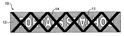
Figure 1 shows an example of a prior art CleartextO
security element 10. The security element 10 comprises a
water impermeable light transmitting plastic carrier
substrate on to which is deposited a thin opaque
aluminum metal layer 12. The metal layer 12 is then
partially removed by a demetallisation process such as, for
CA 02703342 2012-05-23
WO 2009/053673
PCT/GB2008/003505
8
example, direct etch, and resist and etch, to leave metal
free, or substantially metal free, areas 13. Such security
elements 10 having negative indicia are described in detail
in EP-A-319157 and suitable demetallisation techniques
described in EP-A-330733 and US-A-4652015. It has also been
suggested that the metallic negative indicia may be
provided using conductive or non-conductive metal-effect
inks. Whilst this is possible, it is not considered to be
particularly secure or desirable though. For the purposes
of the present invention, the use of vacuum metallised, and
demetallised, layer is preferred, although the use of
printed metal effect layers is also recognized as possible.
Whilst it is preferred that the areas 13 are metal free, it
is possible to leave a very thin layer of metal which
transmits sufficient light such that the indicia are still
visible.
The security feature provided by the security element
10 of the present invention has three elements; a high
reflection layer defining first indicia, a first partial
light scattering layer forming further indicia and a
further light scattering layer. The high reflection layer
is preferably provided by the metal layer 12 of the
security element 10 described above and the additional
layers will be described below.
Figure 2a is a plan view of a first embodiment of the
present invention in which a security element 10 of the
type described in EP-A-319157, and illustrated in Figure 1,
comprises a carrier layer provided with a first partial
light scattering layer 14 which is present in a localized
CA 02703342 2012-05-23
WO 2009/053673
PCT/GB2008/003505
9
area, for example as a simple geometric pattern. Figure 2 b
has been drawn such that the partial light scattering layer
14 and its relationship with a demetallised design, formed
by the metal-free areas 13, can be visualized.
The security element 10 can be partially or wholly
embedded into a security substrate, such as paper used to
manufacture secure documents, in one of the conventional
formats known in the prior art. The wholly embedded
security element 10 is covered on both sides by the base
substrate and the partially embedded element 10 is visible
only partly on the surface of the document in the form of a
windowed security element. In the latter construction the
security element appears to weave in and out of the
substrate and is visible in windows in one or both surfaces
of the document. One method for producing paper with so-
called windowed threads can be found in EP-A-0059056. EP-A-
0860298 and WO-A-03095188 describe different approaches for
the embedding of wider partially exposed elements into a
paper substrate. Wide elements, typically having a width of
2-6mm, are particularly useful as the additional exposed
element surface area allows for better use of optically
variable devices, such as that used in the present
invention. Security elements are now present in many of the
world's currencies as well as vouchers, passports,
travellers' cheques and other documents. In this embodiment
the paper substrate covering the security element provides
the required further scattering layer.
When the security substrate is viewed in transmission
the security element 10 has substantially the same
CA 02703342 2010-04-22
WO 2009/053673
PCT/GB2008/003505
appearance to that of the prior art Cleartext0 element,
i.e. the negative text reading "PORTALS" is highly visible.
However when a non-windowed side of the substrate is viewed
in reflection the viewer is able to visualize the geometric
5 pattern formed by the partial light scattering layer 14.
The geometric pattern may be related to a print design to
be provided on a substrate (in which the security element
10 is embedded) subsequently or could be unrelated. The
present invention makes a benefit of the visualization of
10 the light scattering material and additionally still
retains all the benefits of the known Cleartext0 element.
The manner in which the partial light scattering layer 14
is applied does have to be carefully considered to ensure
adequate visualization of the pattern but without the
pattern detracting from any print or other information to
be provided on the surface of the substrate subsequently.
The visualisation of the partial light scattering
layer 14 when the security element is provided with a
further light scattering layer can be explained with
reference to Figure 2b. Figure 2b shows a part of the
security element 10 embedded into a paper substrate 30 such
that one side of the security element 10 is exposed in
windows 31 in the paper substrate 30 and the other side of
the security element 10 is fully covered by the paper
substrate 30. In this example the further light scattering
layer is provided by the paper substrate 30 into which the
security element 10 is partially embedded.
Light impinging on side B of the security element 10
passes through the paper substrate 30 which acts as the
ak 02703342 2010-04-22
WO 2009/053673
PCT/GB2008/003505
11
further light scattering layer where it is scattered to
some extent. Where light is incident on the metal
reflection layer 12 not covered by the light scattering
layer (interface C), it is reflected back into the paper
substrate 30 and then undergoes further scattering before
exiting the paper substrate 30. In this case the light
exiting the paper substrate 30 will be more diffuse than
that incident on the paper substrate 30 due to the
scattering effect of the paper substrate 30. Furthermore
the reflected light will have lost some intensity when
reflected at the metal interface C. This could equate, for
example, to a 5% loss in intensity.
In contrast, where light is incident on the partial
light scattering layer 14 it undergoes scattering when
travelling both through the paper substrate 30 and the
partial light scattering layer 14. The presence of the
partial light scattering layer 14 will result in a
proportion of the light reflected from the metal interface
D being scattered back towards the metal interface D and
undergoing multiple reflections at the metal interface D
resulting in a loss of intensity (for example 5%) each time
this occurs before finally exiting the substrate 30. The
combination of intensity losses generated by the scattering
of light from the paper substrate 30 and the partial light
scattering layer 14 results in a significant reduction in
the intensity of the reflected light from the regions of
the security element 10 where the partial light scattering
layer 14 is present compared to the regions 14a where the
localised light scattering layer 14 is not present. This
reduction in intensity results in the indicia formed by the
CA 02703342 2012-05-23
WO 2009/053673
PCT/GB2008/003505
12
partial light scattering layer 14 appearing relatively dark
when viewed from the non-window side 33 of the security
substrate 32 in Figure 2a.
The further scattering layer may also be included in
the security device 10 rather than making use of the
scattering properties of the substrate 30 in which it is
embedded. For example it is customary practice for security
elements 10 having a width greater than approximately 2mm
to hide surfacing of the security element 10 from the
embedded paper side by using a masking coat on the security
element 10. A suitable material for such a masking coat
would be Coates 3188XSN or Coates HeliovyPWhite S90 353. A
typical coat weight is suggested to be in the region of
2GSM. Such a masking coat has similar scattering properties
to paper such that light reflected from the security
element 10 appears diffuse and has a paper like appearance.
Suitable light scattering layers 14 for use in the
present invention include matt varnishes or lacquers and
matt embossed structures. As highlighted above it is
possible to provide light scattering layers 14 with
additional machine detectable functionality, for example
magnetic properties. Although it should be noted that, in
this latter example, the magnetic materials used and their
loading in an ink needs to be carefully controlled in order
to achieve the necessary transparency and machine
readability.
Any scattering layer could be used for the further
scattering layer including the examples listed herein below
for light scattering layer 14. However it is preferred if
Trademark
ak 02703342 2010-04-22
WO 2009/053673
PCT/GB2008/003505
13
the further light scattering layer is sufficiently
diffusing to provide a paper-like appearance.
It has been found that a surface area coverage for the
light scattering layer 14 should be less than 70%,
preferably less than 60%, and more preferably less than 50%
of the overall thread surface area on one side. For non-
magnetic light scattering layers 14 this is predominantly
driven by aesthetic considerations. Whereas the surface
area coverage set out above is suitable for meeting both
the machine detection requirement and providing the
visibility of the security element 10 in reflection when
embedded in paper when using magnetic light scattering
layers 14. However even lower surface area coverage can be
achieved by providing a thicker magnetic light scattering
layer 14 or by increasing the percentage magnetic material
loading in the ink used as the magnetic light scattering
layer 14. Use of too high a surface coverage of light
scattering magnetic or non-magnetic material results in the
security element 10 appearing as a substantially solid dark
line which is not desirable.
Non Magnetic Light Scattering Layers
In these embodiments of the invention the scattering
layer 14 takes the form of a matt varnish or lacquer which
can be applied using one of the standard security printing
processes. One example of a suitable matt varnish is a
suspension of fine particles in an organic resin. The
surface particles scatter the light as it passes through
the varnish resulting in a matt appearance. The scattering
CA 02703342 2010-04-22
WO 2009/053673
PCT/GB2008/003505
14
process can be enhanced by the particles migrating to the
surface of the varnish or lacquer when is applied to the
carrier 11 or vacuum metallised layer 12. The surface
particles scatter the light as it passes through the
varnish resulting in a matt appearance. Suitable particles
include silica based materials but it should be recognized
that any particulate material could be used that causes a
scattering of light but which does not detract from the
transparency of the coating when it is applied to the
security element 10. An example of a material suitable for
forming a light scattering layer 14 is a screen printable
matt varnish comprising 5% TS200 Silica Matting Agent from
Degussa and 95% 5X383 Solvent-Based Nitrocellulose Screen
Varnish from Sericol.
In an alternative solution the fine particles can be
replaced by organic waxes.
As a further alternative, the light scattering layer
14 can be generated by embossing a matt structure into the
surface of the vacuum metallised layer 12. Such matt
structures should typically comprises characters or
patterns wherein the surface of the embossing is provided
with a rough surface such that light impinging on the
surface is reflected off in a diffuse non-specular manner.
As an alternate the embossings themselves may be lines or
dots of differing angles or sizes distributed so as to
create a light scattering pattern.
Magnetic Light Scattering Layers
CA 02703342 2010-04-22
WO 2009/053673
PCT/GB2008/003505
It has been found that certain new magnetic materials
are particularly suitable for the present invention,
although this does not preclude the use of more
conventional heavily coloured conventional magnetic
5 materials, such as iron oxides (Fe203, Fe304), barium or
strontium ferrites etc.
The new materials have particular magnetic properties
which allow them to be distinguished from other magnetic
10 materials. In particular, these materials have a lower
coercivity than conventional iron oxide materials which
means that they can be reversed in polarity by weaker bias
magnetic fields during the detection process; whilst they
are still magnetically hard so that they retain the induced
15 magnetism which can then be detected when the article is in
a region no longer affected by the bias magnetic field.
Typically, these materials can support magnetic data in the
same manner as conventional magnetic tape.
Suitable new magnetic materials for the security
element 10 preferably have a coercivity in the range 50-
1500e, and more preferably in the range 70-1000e. The
upper limit of 1500e could be increased with higher biasing
fields. A number of examples of suitable materials include
iron, nickel, cobalt and alloys of these. In this context
the term "alloy" includes materials such as Nickel:Cobalt,
Iron: Aluminium:Nickel:Cobalt and the like. Flake Nickel
materials can be used; in addition Iron flake materials are
suitable. Typical nickel flakes have lateral dimensions in
the range 5-50 microns and a thickness less than 2 microns.
CA 02703342 2010-04-22
WO 2009/053673
PCT/GB2008/003505
16
Typical Iron flakes have lateral dimensions in the range
10-30 microns and a thickness less than 2 microns.
The preferred new materials include metallic iron,
nickel and cobalt based materials (and alloys thereof)
which have amongst the highest inherent magnetisations and
so benefit from the requirement for least material in a
product to ensure detectability. Iron is the best of the
three with the highest magnetisation, but nickel has been
shown to work well from other considerations. These
materials are best used in their flake aspect to ensure
that they are high remanence, hard magnetic materials that
can support magnetic data if used in a magnetic tape
format. This is because nickel and iron, for example, in
flake form generally have high remanence. Flake and other
shaped materials provide an anisotropy (Kshape) defined as:
Kshaps = 0.5 Nd M2/1-lo
While
a 2 - Ktotal/Ms
Leading to a coercivity H which is proportional to Ms
and Nd (See "Magnetism and Magnetic Materials", J P
Jakubovics, Uni Press Cambridge, end Ed.)
Where:
Nd is the shape factor
Ms is the saturation magnetism
Po is the permeability of free space
H is the coercivity
Ktotai is the sum of all K components
CA 02703342 2010-04-22
WO 2009/053673
PCT/GB2008/003505
17
It should be understood, however, that it may not be
essential to take account of this shape effect for a
material to exhibit low coercivity and high remanence. For
example, the crystalline anisotropy of materials can also
lead to a high remanence, hard magnetic low coercivity
characteristic even if the material has a spherical shape,
for example cobalt treated oxides.
A suitable new magnetic ink composition for use with
the present invention can be obtained from Luminescence Inc
as 60681XM.
Conventional magnetic inks, with the common Fe203 or
Fe304 pigments or similar, can, for example, be obtained
from Luminescence Inc as RD1790.
The magnetic ink is applied to the security element 10
to form layer 14 during manufacture using any of the known
printing and transfer techniques including for example,
gravure, intaglio, lithography, screen, and flexography.
Figure 3 shows a cross section through a security
element 10 according to the present invention illustrate a
construction for a simple magnetic, partially demetallised
security element 10.
A first element 10a is first produced by a known a
demetallisation technique as discussed above and comprises
a plastic carrier substrate lla of polyethylene (PET) and a
metal layer 12 with metal free areas 13. Figure 3 shows a
CA 02703342 2012-05-23
WO 2009/053673
PCT/GB2008/003505
18
resist layer 15 resulting from a resist and etch technique,
but the resist layer 15 will not be present if one of the
other techniques described above are used. A second element
10b is produced, also comprising an impermeable plastic
carrier substrate 11b, such as polyethylene(PET). A
partial light scattering layer 14 of a magnetic material is
printed on this carrier substrate 11b, as described above.
This magnetic partial light scattering layer 14 can also be
printed on the reverse side of the first element 10a; in
which case a primer layer may be required. In the example
shown in Figure 2, the magnetic partial light scattering
layer 14 has been applied in a cross-hatch pattern. This
pattern results in the security element 10 having a
coverage of magnetic material of less than 50%. The first
and second elements 10a, 10b are laminated together to form
the security element 10 using a suitable laminating
adhesive 16, an example of which is NovacoteI10-2525/3346.
One or more further water based adhesive (e.g. National
Starch & Chemical Eclipse 033-4172) layers 17 is/are
applied to the security element 10 to aid its adhesion when
embedded in a security substrate 30.
The embodiment of the security element 10 shown in
Figure 4 is similar in construction to that illustrated in
Figure 3, but without the second carrier substrate 10b.
This is a less costly construction in terms of materials,
but the security element 10 can be more vulnerable to
environmental attack in service, unless the correct
materials choices are specified to enhance durability. A
particular advantage of this is that it makes the
#Trademark
CA 02703342 2012-05-23
WO 2009/053673 PCT/GB2008/003505
19
production route and construction consistent across the
bulk of security element types and manufacturing routes.
An example of a particularly suitable PET material
consistent with this single PET layer design requirement is
Mylaj-813 from Du Pont with the pretreated side available
for the magnetic partial light scattering layer 14. This
particular material, and others of a similar nature, allow
fully durable externally printed magnetic coatings that
resist the standard conventional security paper hazard
testing and washing machine durability requirements.
In Figures 3 and 4, the security elements 10 have a
white or coloured masking coat 18. The presence of the
masking coat 18 provides a further scattering layer in the
device structure resulting in the presence of the magnetic
partial light scattering layer 14 being visualised as a
dark image when viewed in reflection from the reverse side
of the security element 10. If this security element 10 is
subsequently embedded into a paper substrate 30 the
visibility of the magnetic partial light scattering layer
14 will be further enhanced by the scattering properties of
the paper. This masking layer 16 may also include
fluorescent pigments.
Alternatively the masking layer 18 can be omitted from
the structures as the magnetic partial light scattering
layer 14 will still be visualized when embedded or
partially embedded into the paper substrate 30 due to the
scattering properties of the paper.
**Trademark
CA 02703342 2012-05-23
WO 2009/053673
PCT/GB2008/003505
Figures 5 to 11 show various other examples of how the
magnetic partial light scattering layer 14 can be applied
to the security element 10. In Figure 6 magnetic material
has been applied as a complex geometric pattern. Such
5 patterns may be designed such that they mirror or
complement the guilloche patterns commonly used on a wide
range of security documents.
In Figure 7 a magnetic ink has been printed as a
10 repeating scripting reading -PORTALS-. This embodiment
provides a very strong combination feature with the
negative script present in the metal layer 12. In
reflection a viewer would see the positive text reading
"PORTALS" and then in transmission they would see the same
15 or an alternate negative script resulting from the
demetallised layer 12/13.
In Figure 8 a magnetic material has been applied in
the form of a signature. This signature may be a monarch,
20 the Governor of a National Bank or, where there is a
portrait present on the note, the signature of the
individual portrayed. For banknotes (made from security
substrates), the use of the Governor of the National Bank's
signature is preferred as their signature is also usually
printed on the banknote. The viewer can then compare the
signature on the security element 10 with that on the
printed surface of the banknote.
In Figure 9 the magnetic material has been applied as
a solid area with negative script present. In this example
the viewer would visualize negative script in both
CA 02703342 2010-04-22
WO 2009/053673
PCT/GB2008/003505
21
reflection and transmission. As with previous examples the
script can take any form or design and be the same or
different to that provided by the demetallised pattern
viewable in transmitted light.
In Figure 10 the magnetic material has been applied as
a company logo. As an alternative to company logos, other
identifying information could be used, such as national
insignia, animals, flowers etc. This provides another
strong link to the security document and another means to
aid the authentication of the security device for the
public.
In Figure 11 the magnetic material is printed so as to
provide denomination information.
Figure 12 shows a detailed cross section through a
further embodiment of a security element 10 according to
the present invention. In this embodiment the security
element 10 is provided with a liquid crystal layer 20. The
security element 10 is further provided with a dark
absorbing layer 21 that co-operates with the liquid crystal
layer 20 to provide a strong colourshifting effect with
varying angle of viewing. In a preferred example a polymer
liquid crystal is used, but an alternate example makes use
of liquid crystal inks such as those supplied by Sicpa
under the brand name OasisTM. The absorbing layer 21 is
preferably a layer of dark or black resist in the etching
of the metal layer 12.
CA 02703342 2010-04-22
WO 2009/053673
PCT/GB2008/003505
22
Figure 13 shows a security element 10 provided with an
embossing lacquer layer 22 which is embossed with a
diffractive or holographic relief pattern.
Figure 14 shows an embodiment comprising a metal
dielectric thin film colourshifting security element 10
having a dielectric layer 24 and absorber layer 25.
As an alternative to printing the light scattering
layer 14a embossed matt light scattering structures can
also be used. Embossed matt light scattering structures
cause incident light to be reflected non-specularly or
diffusely.
The embossed light scattering structures can comprise
lines and take any convenient form including straight
(rectilinear) or curved such as full or partial arcs of a
circle or sections of a sinusoidal wave. The lines may be
continuous or discontinuous and, for example, formed of
dashes, dots or other shapes. By other shapes we mean the
dots or dashes could have a graphical form. The line widths
are typically in the range 10-500 microns, preferably 50-
300 microns. Preferably, the individual lines are barely
visible to the naked eye, the main visual impression being
given by an array of multiple lines. The lines can define
any shape or form, for example square, triangle, hexagon,
star, flower or indicia such as a letter or number.
The embossed line structures are preferably formed by
applying an embossing plate to the security element under
CA 02703342 2010-04-22
WO 2009/053673
PCT/GB2008/003505
23
heat and pressure. Preferably the embossing process is an
intaglio printing process and is carried out using an
intaglio plate having recesses defining the line
structures. Preferably the security element is blind
embossed, i.e. the recesses are not filled with ink.
The height of the embossed areas should be at least
2pm but preferably greater than Spm and more preferably
greater than lOpm.
In a further embodiment of the present invention the
security device is incorporated into a polymeric banknote.
Polymeric banknotes, such as those described in WO-A-
8300659, are formed from a transparent substrate comprising
at least one layer of an opacifying coating on both sides
of the substrate. The opacifying coating is omitted in
localised regions on both sides of the substrate to form a
transparent region known as a window. In this embodiment of
the present invention the security deice is formed in a
selected region on the transparent substrate of the
polymeric banknote by applying a metallic layer and a first
light scattering layer in the same manner as described
previously. In this manner the transparent substrate of the
polymeric banknote also acts as the light transmitting
carrier substrate for the security device. The opacifying
coating is then applied to the transparent polymeric
substrate over the security device and functions as the
further light scattering layer.
CA 02703342 2010-04-22
WO 2009/053673
PCT/GB2008/003505
24
Polymeric banknotes are just one example of a secure
document based on a polymeric substrate, the current
invention is equally applicable to other types of polymeric
secure documents.